Comparison of Fault-Tolerance Techniques for Massively Defective Fine- and Coarse-Grained Nanochips Jacques Henri Collet1, Mihalis Psarakis2, Piotr Zając1,3, Dimitris Gizopoulos2, and Andrzej Napieralski3 1) Laboratoire d'Analyse et d'Architecture des Systèmes du CNRS, 7 avenue du colonel Roche, Université de Toulouse, 31077, France. e-mail:
[email protected]
2) Computer Systems Laboratory, Department of Informatics University of Piraeus, 80 Karaoli & Dimitriou Street 18534, Piraeus, Greece. e-mail: {mpsarak, dgizop}@unipi.gr
3) Department of Microelectronics and Computer Science, Technical University of Lodz, Al. Politechniki 11, 93-590 Lodz, Poland. e-mail: {pzajac, napier}@dmcs.pl
Abstract— The fundamental question addressed in this paper is how to maintain the operation dependability of future chips built from forthcoming nano- (or subnano-) technologies characterized by the reduction of component dimensions, the increase of atomic fluctuations and the massive occurrence of physical defects. We focus on fault tolerance at the architectural level, and especially on fault-tolerance approaches, which are based on chip selfdiagnosis and self-reconfiguration. We study test and reconfiguration methodologies in massively defective nanoscale devices, either at fine granularity field programmable devices or at coarse granularity multi-core arrays. In particular, we address the important question of up to which point could future chips have self-organizing fault-tolerance mechanisms to autonomously ensure their own dependable operation. In the case of FPGAs, we present known fault tolerant approaches and discuss their limitations in future nanoscale devices. In the case of multicore arrays, we show that such properties as self-diagnosis, selfisolation of faulty elements and self-reorganization of communication routes are possible. Index Terms— Nanotechnology, diagnosis, testing, reconfiguration, fault tolerance, FPGA, multicore architectures
I. INTRODUCTION We study the challenges of fault tolerance and dependability improvement for chips built in massively defective technologies (MDT). In both emerging nanoelectronics beyond CMOS and in technologies based on molecular electronics, the extreme downsizing of transistor dimensions increases the impact of process variations [1,2], and ultimately increases the probability of permanent and transient faults at gate level. Consequently, chip dependability is clearly one of the major challenges of all future nano- (or subnano-) technologies and should be taken into consideration from the very beginning in the process of chip design. The main problem of future MDT is how to ensure the dependable operation of Ultra Large Scale Integration (ULSI) chips. In today's weakly-defective technologies, chip dependability is mostly achieved at transistor or (and) circuit level and is essentially guaranteed by a chip validation test at the end of the fabrication process. However, as the defect rate
constantly and inevitably rises due to downsizing, this approach will be more and more difficult to maintain, i.e., guaranteeing the dependable continuous operation by the sole implementation of fault-tolerant techniques at the circuit level may become problematic if not impossible. Therefore, one should plan integrating fault-tolerant techniques at coarser granularity (i.e., at the architectural level and thread level), which means that a fraction of chip’s processing should be dedicated to execute some test-related applications (or to modify the execution of user applications) and detect the occurrence of errors caused by permanent and transient faults. In what follows, we shall restrict our analysis to fault tolerance at the architectural level. Actually, the complete description of fault tolerance from the circuit to the thread level is far beyond this paper. In this paper, we focus on the following questions: How to tolerate faults at the architectural level? Architectural-level fault tolerance can be achieved either by redundancy-based techniques or by test and reconfiguration techniques. - Modular redundancy (MR) which has been extensively investigated automatically supports the concurrent detection and masking of errors occurring in one of several modules. One may distinguish fine-grain redundancy at gate level as suggested by von Neumann [3,4,5,6] and block redundancy associated with majority-voting gate, which must be implemented at coarser granularity to ensure that the fault probability of the voter is much smaller than that of protected blocks. It is important to stress that MR is implemented systematically (not to say blindly) to tolerate faults occurring in unidentified positions in the circuitry. A natural consequence of this approach is that all elements are protected, including those, which are fault-free, resulting in high circuit overhead. Moreover, it requires high redundancy level when the fault probability of the protected blocks increases. For these two reasons MR sacrifices lot of gates [7,8,9]. For instance, redundancy levels as high as hundreds or thousands are considered [10 -12]. In this context, one may wonder what could be the interest of evolving toward increasingly defective technologies if the additional elements (transistors, gates, etc.), enabled by the reduction of dimensions, would be mostly 11
invested in protection circuitry to improve the dependability but not the circuit performance. Perhaps a more logical approach would be to use redundancy to protect only the most critical parts of a circuit or architecture to maintain the reliable operation of elements of critical functionality. - Actually, testing is today privileged at the architectural level. In the test/reconfiguration approach, basic blocks are first tested to check whether they operate correctly and to build a map of defective blocks in the chip. Then, it is necessary to build a reliable processing system from the good blocks only (i.e., block deemed as fault-free by the test), discarding those considered as faulty. The question of test granularity is very important. The dilemma may be summarized as follows: the smaller the size of basic blocks, the simpler test is in principle, and the higher fault coverage, but as the tested blocks have limited processing capability, the second phase of organization is more complicated. Field programmable gate arrays (FPGAs) are typically representative of circuits with fine-granularity testing requiring a complex reorganization phase. On the other hand, when basic blocks are sophisticated, test is complicated, fault coverage decreases, but the reorganization process following the test phase is relatively simple. This second case is typical for multicore arrays. In particular, there is no need for constructing processing units by assembling basic blocks as each good basic block (i.e., each core) is itself a generalpurpose processing unit. Consequently, the organization phase is mostly based on creating the reliable communication system, i.e., on guaranteeing the exchange of data among cores in the array. Another critical question of the test/reconfiguration approach is to decide who tests blocks and who is responsible for the reorganization of the chip following the test? For a long time, test and reconfiguration were executed by means of an external test controller. However, this approach is not scalable and will lead to increasing number of problems in the forthcoming technologies. So, a general trend consists in embedding test circuits on chip. It is already implemented in the latest generations of memories. Ultimately, this approach could be also generalized to the processing parts of chips which leads us to the central question of this paper which is: to which extent, chips could exhibit self-organization mechanisms to maintain autonomously their operation dependability? The paper is organized as follows. In section II, we present known fault-tolerance approaches at fine-grain level, i.e., in FPGA chips. We describe various test and reconfiguration techniques and discuss their limitations in future nanoscale FPGAs. Similarly in section III, we analyse the test/ faulttolerance approach at coarse-grain level, i.e., in multicore chips. We show how faults can be tolerated and that multicore arrays can become almost autonomous, with self-organizing and fault tolerant properties. II. FAULT TOLERANCE AT FINE ARCHITECTURAL GRANULARITY A. Introduction In this section, we consider the most popular reconfigurable technology, the Field Programmable Gate Arrays (FPGAs). A typical FPGA architecture consists of an array of
programmable logic blocks (PLBs) interconnected by a programmable routing network. An FPGA configuration defines the user application implemented by the programmable device. A fault tolerant scheme must protect the FPGA against possible faults at any device resources: PLBs, interconnection network, and configuration memory. An application designer can use a commercial FPGA and implement his own fault tolerant scheme to build a dependable FPGA application, for example a static hardware redundancy method like Triple Modular Redundancy (TMR) can be applied in the original design before its mapping to the FPGA fabric. Several redundancy-based fault tolerant techniques have been proposed for FPGAs that mainly cope with transient errors (single-event upsets, SEUs). The most common SEU mitigation techniques are mainly based on redundancy techniques. However, in future nanoscale FPGAs with high defect density, the redundancy-based methods like TMR or NModular Redundancy (NMR) will result in high redundancy level and thus in high area and power overheads. On the other hand, the ability of FPGAs for reconfiguration provides an interesting opportunity for fault tolerant techniques that will be based on fault diagnosis and reconfiguration. The key idea behind such fault tolerant techniques is that reconfigurability allows first to detect and locate the defective parts and then to configure the device to avoid them. Since the diagnosis and avoidance of defective parts can be performed at fine granularity, we characterize these techniques as fine-grain fault tolerant techniques. Furthermore, an FPGA-based application includes an inherent redundancy, since, in most cases not all the available FPGA resources are used from the user application or many PLBs are partially used. It is therefore practical a fault tolerant technique to exploit the unused resources (PLBs or interconnects) to replace defective parts. The fine-grain fault tolerant techniques comprise two steps: fault diagnosis and fault recovery. In the following subsections we discuss known fault diagnosis (section II.B) and fault recovery methods (section II.C). B. Fault diagnosis in FPGAs Fault diagnosis methods can be divided into two main categories: (a) off-line BIST methods and (b) roving test methods. Off-line BIST methods [13] load one or more test configurations that test the logic and the interconnection of the FPGA. The test configurations, called test sessions, are loaded off-line. Each test session configures a group of PLBs as test pattern generators (TPGs) and output response analyzers (ORAs) and another group of PLBs as blocks under test (BUTs). BUTs are reconfigured in different modes of operation in order to be completely tested. After the end of the first test session, a second test session is initiated where the PLBs have exchanged roles: PLBs previously configured as BUTs become TPGs or ORAs and vice versa. Thus, within two sessions all PLBs have been configured as BUTs and thus have been tested. To provide accurate diagnosis of faulty PLBs, some approaches proposed the execution of more test sessions. The accurate diagnosis of defective parts at the finest possible granularity helps fault recovery methods to achieve higher yield improvement. The only overhead of the BIST
methods is the requirement for storage the different test configurations. Many BIST approaches have been proposed targeting the diagnosis of different FPGA fabric resources, i.e. look-up tables [14], or interconnects [15]. These approaches are evaluated in terms of test coverage, test duration and memory overhead. A weakness of these approaches that will be accentuated in the future massively defective FPGAs is that they are not able to locate faults in a FPGA device that has both faulty PLBs and faulty interconnects [13]. Roving test methods [16], [17] perform a progressive online scan of the FPGA fabric exploiting the device capability for run-time partial reconfiguration. These methods use small roving Self-Testing Areas (STARs) which are configured to be tested off-line while the remaining FPGA logic continues its normal operation without interruption. Since the testing of the STARs is completed then they move (rove) in new locations; before that a portion of the normal application logic has been copied in the blocks previously occupied by STARs. Roving test methods can be also applied for on-line fault diagnosis and have much lower area overhead than redundancy methods. They also provide high fault coverage and diagnosis granularity comparable to BIST methods. Recent roving methods propose more efficient BIST designs achieving higher diagnostic coverage (diagnostic coverage is the percentage of faults correctly diagnosed), for example approach [17] achieves 88% diagnostic coverage at 25% fault density, while a previous approach [16] achieve 55%. It is obvious that as the defect density increases the diagnosis accuracy of roving methods will be reduced. C. Fault tolerance in FPGAs Fault tolerant techniques can be divided into two main categories depending on the level of FPGA architecture that faults are tolerated: (a) device-level and (b) configurationlevel. A survey of fault-tolerant techniques for FPGAs can be found in [18], [19]. Device-level fault tolerant techniques isolate the defective FPGA resources by permanent organization changes at the hardware level. They build an apparently fault-free array from a larger array, which contains defective resources. When a defective part is diagnosed, the self-repair control logic makes permanent routing and/or logic changes in the FPGA fabric replacing the defective part with spare hardware resources. Note that the device preserves its original size and organization of logic array and interconnects. The key advantage of these techniques is that the fault recovery process is transparent to the end-user tools. The traditional device-level approaches use spare rows and columns [20] and tolerate the defects bypassing the entire defective row or column. Such coarse-grain approaches make waste of fault-free resources and have limited flexibility to tolerate multiple, distributed defects. Other fine-grain approaches integrate more bypassing alternatives providing greater flexibility for the recovery of multiple defects and making more efficient use of spare resources [21]. The drawback of device-level approaches is that for a given number of spare recourses they can tolerate a bounded number of defects and that their applicability depends on the
distribution of defects; there are certain patterns of faults even in low-defect densities which cannot be tolerated. Thus, in order to be viable in future nanoscale FPGA devices with high defect densities they have to impose significant overhead for spare logic and routing resources. Configuration level fault tolerant techniques exploit the availability of resources not used by the application and tolerate faults at the level of FPGA configuration replacing the defective parts with the unused resources. The placement-androuting tools know the location of defects and select fault-free resources to layout the circuit to the FPGA fabric. The main drawback of this category is that an external controller is required to run the implementation tools and calculate the new FPGA configuration, so self-configuration is not feasible. Thus, most configuration level approaches attempt to reduce the external computing effort mainly by implementing incremental placement and routing. Representative approaches of this category are the pebble shifting [22] and cluster reconfiguration [23]. Pebble shifting perturbs an initial design configuration in order to move parts of the circuit away from defective resources. In cluster-based FPGAs, a cluster reconfiguration approach replaces faulty clusters with faultfree spare clusters. The incremental approaches, especially those which combine the two above methods, cope well with high fault densities and random fault distribution. Another approach [24] reduces the run-time computational effort using precompiled configuration. It splits the FPGA into tiles where each tile is composed of a set of physical resources and an interface to the adjacent tiles. Fault tolerance is achieved by providing multiple precompiled alternative configurations of each tile. Each configuration places spare logic in a different location inside the tile while maintaining the same tile external interface. When a fault is detected within a tile, the configuration tile is replaced by an alternative configuration which does not use the faulty resources. Since the placement-and-routing has already done, this approach requires less processing power to compute the new configuration. This is achieved at the expense of larger configuration bit files, which include all the alternative configurations. Another disadvantage is the limited number of defects and distributions that can be tolerated. D. Limitation of the fine-grain fault tolerant approaches The fault diagnosis process in FPGA chips has matured in the last years; the recent off-line BIST and on-line roving diagnosis approaches achieve high defect coverage and precise fault location and they might be as well applied to future nanoscale FPGAs. However, the known fault recovery approaches can not guarantee a self-organizing fault-tolerance for the massively defective FPGA chips. On the one hand, the device-level approaches can tolerate only a bounded number of defects with specific defect distribution and thus they can not be considered as an adequate fault tolerant solution for the future nanochips. On the other hand, the configuration-level approaches do not enable a fully autonomous approach since they require external control for the execution of placement-and-routing algorithms and the calculation of the new configuration. We can achieve a
trade-off between fault tolerance level and external computational effort using different granularity levels. A coarse-grain approach requires less complex algorithms for the computation of the new configuration but it wastes more faultfree resources and thus it is relatively intolerant to a defect density increase. On the contrary, a fine-grain approach needs less spare resources to tolerate high defect densities but requires complex external control. We believe that to achieve a high degree of autonomous fault tolerance to massively defective future FPGAs a more radical approach should be adopted, like the one proposed in [25] which has been inspired from biology. In [25], the authors dynamically adapt the construction of an electronic circuit to hardware defects by formulating the process as a series of interactions between identical but specialized structures, called supercells (supercells have the possibility to reconfigure their neighbours). They describe an adaptive configuration process for a reconfigurable platform, called Cell Matrix, which takes care of chip testing and performs placement and routing avoiding defective regions. III. DEPENDABILITY AT COARSE ARCHITECTURAL GRANULARITY A. Introduction In this section, we consider general-purpose multicore chips where the processor cores and the routers are the basic building blocks. Multicore architectures have emerged as a "simple" solution to organize the sea of transistors enabled by the technology advances and in particular by the reduction of transistor dimensions. Indeed, it is an economical method to solve the complexity in the circuit or in the architectural layers, although it generates many problems in the upper layers, especially regarding the scheduling, the parallelization of tasks and the execution of multithreaded applications. The choice of the physical organization of a multicore chip is crucial in this context. Two architectures practically prevail. The bus-based or crossbar-based topologies are commonly preferred when the number of cores is small, say typically lower than 32. However these architectures are not scalable. Consequently, scalable arrays (i.e., 2D-mesh, torus, two-layer architectures) are used for larger multi-node systems. In what follows, we consider arrays as the long-term solution to interconnect a large number of cores. Moreover, regular arrays are intrinsically highly fault-tolerant since, due to their topological symmetry, there is no critical and indispensable element, as for example in crossbar-based architectures, where the crossbar switch itself is not replicated and thus should be protected or specially designed to tolerate internal physical faults. Chip dependability results from the conjunction of a diagnosis phase (to identify the defective parts, described below in section B) followed by the execution of reconfiguration actions (to isolate the parts diagnosed as faulty and to maintain the communication in the array, described in section C) and ultimately on-the-fly processing decisions at runtime to cope with transient faults and faulty but incorrectly diagnosed as fault-free parts.
B. Testing in Multicore Arrays We review in this section the methods currently used in unicore processors testing, and their evolution to diagnosing cores in multicore arrays. We describe successively the external test, the built-in self test, the software-based self test, and the mutual test. 1) External test: It has been implemented for decades. These test practices can be generally categorized to functional test approaches, where the functionality of the processor chip is verified at normal operating mode through its external interface and to structural test approaches, where internal blocks or structures of the chip are tested separately at special test modes. The external functional testing is usually performed by big-iron functional testers connected at the processor pins, while the structural testing solutions, like scan-based approaches improve the accessibility of the internal processor nodes involving design-for-testability (DfT) techniques and relax the requirements for high-cost testers. However, the hardware overheads of the DfT modifications, the performance degradation, and the excessive power consumed during special test modes are sometimes not acceptable for carefully optimized designs like processors. Moreover, the scan-based techniques can not catch defects which are manifested when the chip operates at its actual speed. 2) Built-In Self Test (BIST): In fact, the increase of chips complexity makes external functional test not scalable in the long term. For the above reasons, self-test approaches have been adopted which move the test functions from external testers to on-chip resources achieving at-speed testing and reducing the overall test cost. Hardware-based built-in selftest has been efficiently applied to regular structures, like memory arrays [26] or embedded arithmetic units. 3) Software-based Self-Test (SBST): Traditional, hardware BIST techniques are an ideal solution for components with a regular architecture. However, the application of hardware-based BIST techniques to processor cores [27] requires extensive design modifications to make the circuit BIST-ready. Thus, Software-based self-test (SBST) [28] has gained increasing acceptance during the last decade and currently forms an integral part of the processor manufacturing test process. The key idea of SBST is to exploit the on-chip programmable resources to run self-test programs: test patterns are generated and applied by the processor itself using its native instructions, virtually eliminating the need for additional test-specific hardware. In a typical SBST flow, the test programs and data are downloaded into on-chip memories, using a low-speed, low-cost tester. Subsequently, these test programs are executed by the processor at actual/full speed and test responses are stored back in the on-chip data memory from which they can be read out and compared with the correct/expected responses. The main advantages of SBST are the following: • Non-intrusive nature: No extra hardware is required and no extra power is consumed compared to normal operation. • At-speed testing: Test application and response collection are performed at the processor’s actual speed. • No over-testing: Since it is performed in functional/normal mode, it avoids detecting errors that will never occur during the normal processor operation thus increasing yield.
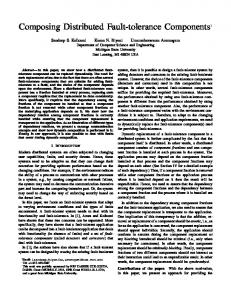
• Reusability: The same self-test programs can be used at manufacturing testing or in-field testing. SBST has been used from simple, low-complexity processors [29] to complex pipelined processors with advanced performance mechanisms [30]. The efficiency of SBST methodology has also been demonstrated for in-field, periodic testing of embedded processor cores targeting permanent and intermittent operational faults [31]. Also, the applicability of SBST to bus-based multiprocessor architectures and the efficient exploitation of execution parallelism have been proved [32]. 4) Mutual test (MT): Self-diagnosis methods described in the previous section are based on the implicit assumption that each faulty core is capable of correctly executing the protection actions. In other words, it is assumed that even when a core is defective, it is still able to detect it and isolate itself from the rest of the array. The mutual diagnosis approach [33,34,35,36] was invented to enable testing of cores without making the above assumption. It is built on top of a self-test method: each core first executes its self-tests (running for example test programs locally stored in node memory or activating a built-in test pattern generator) and generates a test signature. Then, it sends this signature to its four neighbors. As all cores execute separately this procedure, each core may compare its own signature with those received from its neighbors. When a “good” core discovers that the signature from an adjacent core is different from its own one (or when it receives no signature following within some timeout interval), it considers the adjacent core to be faulty and tells its router that all the communication with this node should be stopped. We call it the communication suspension mechanism (CS) or node isolation mechanism. Consequently, the isolation mechanism of bad nodes exclusively relies on the action undertaken by good nodes (i.e., by router/tester pairs) with no hypothesis on the unpredictable behaviors of faulty cores [37, 38]. In order to clarify the above analysis, Fig. 1 below displays a typical example of a chip partitioning achieved by the mutual-test mechanism. The chip is a 7x9 square array including 14 defective black-colored nodes and 4 input-output ports (IOPs, labeled N, E, S, W) positioned in the middle of each array edge. Each node is made up with a core and a router, respectively represented by a square and a circle. The solid lines between two routers show the interconnects. For clarity, we did not draw the interconnects which have been logically disabled following the mutual test mechanism. The clusters of defective cores, isolated from good cores, are enclosed in separate dotted curves. Zones of good nodes enclosing the IOPs are especially important in this approach. Additionally, we stress that: 1. We do not envisage the physical disconnection of faulty routers. A good router simply stops communicating with any adjacent router diagnosed as defective. Consequently, no physical reconfiguration is implemented in the chip and no spare elements are needed as suggested in many previous works [39,40,41,42]. 2. The disconnection mechanism automatically splits the communication array into several zones of faulty and good nodes, regardless of the actions of defective nodes.
N
6 5 4 3
E
W
2 1
S
0 0
1
2
3
4
5
6
7
8
Fig. 1: Example of self partitioning of cores in a 2-D grid architecture resulting from the mutual-diagnosis mechanism. The grid includes a 4-IOP and 14 defective cores.
good core,
faulty core,
router,
IOP.
C. Architectural self-organization Self-organization is the conjunction of 3 mechanisms which are autonomously executed by the chip, namely: mutual test (see the previous section), isolation of faulty parts, and finally self-reorganization of the communication architecture. The great advantage of coarse-grain architectures like the multicore arrays considered in this section is that the chip organization does not need the reconfiguration of the processing elements contrarily to fine-grain architectures like FPGAs described in section II. The sole isolation of the parts diagnosed as defective and the reconfiguration of routes in the existing communication architecture are sufficient. Moreover, these mechanisms can be executed by the chip itself with no external control as it will be shown below. Route discovery in multicore arrays is executed at startup and possibly periodically at runtime. Each IOP executes separately the following route discovery mechanism: Step 1: Each IOP emits a route request message (RR). The message is propagated by means of flooding diffusion, i.e., each node forwards each incoming RR to all links except the incoming link [43]. Flooding protocols enable moving around the disconnected zones, i.e., around zones including cores diagnosed as faulty in the mutual-test procedure described in the previous paragraph and allow discovering routes. The idea here is that each router forwarding a RR adds in the message header the routing which is locally executed (for instance, the index of the output link), so that during propagation, a RR message registers the route which it follows. Step 2: Each good node receiving the RR sends one route acknowledgment message (RA) back to the emitter. Note that the RA may be sent as unicast and simply follow the RR route in the opposite direction. Globally, the number of RAs coming back to the IOP is as large as the number of nodes which can be contacted in the zone of good nodes enclosing the IOP. Step 3: Each IOP collects the RA messages and stores the routes in a dedicated array in its memory, which we call the valid route array (VRA). Thus, at the end of this route discovery phase, each IOP has stored the routes to the cores which it can contact, and each core has
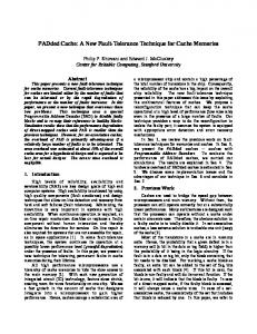
Probability that the IOP reaches more than the fraction fC of cores
D. Limits of the coarse-grain approach An important issue is that after the partitioning of the array, some good nodes may be located outside the zones which comprise IOPs. Consequently, they cannot communicate with the IOPs and cannot take part in the processing allocated by the IOPs. For instance, the dotted loop in the top left corner of Fig. 1 encloses a cluster of three good cores with coordinates (0,5) (0,6) and (1,5), which are inaccessible from the IOPs and therefore cannot be used to execute tasks. To estimate the efficiency of the route discovery mechanism described in section III.C, we studied the reachability, i.e., the fraction fC of good cores that can be contacted versus the fraction of defective cores and the connectivity of the routers. Reachability simulation results are displayed in Fig. 2 and Fig. 3. We used the simulator MASS to conduct this investigation [45]. In each figure, the x axis represents the reachability whereas the y axis represents the probability to exceed this reachability. 1
A
0.94
0.8 2D mesh C=4
PF=0.2
0.6
n=450 0.4
hexagonal C=3
0.2
fraction of faulty cores does not exceed 20%, because very few good cores are inaccessible (3%). However, the 2D mesh topology becomes unsatisfactory when the fraction of defective cores increases as shown in Fig. 3. This figure is similar to Fig. 2 except that the array includes 40% of defective cores. We calculated the probability that the reachability exceeds a definite value in a hexagonal, a square, a torus or a 2-layer mesh topology. The connectivity of most nodes is C=3 in the hexagonal network, C=4 in the 2D-mesh network or the torus, and C=5 in the 2-layer mesh network. The torus is a modification of the mesh network, where in fact there is no border so that all nodes have the connectivity C=4. To enable comparison of the various topologies, the simulations for all networks have been performed for networks with a similar number of nodes. More precisely, the hexagonal network had 450 nodes, the 2-layer mesh network was constructed using two connected 15x15 meshes with a total of 15⋅15⋅2=450 nodes. The mesh and the torus were 21x21 arrays, with a total of 441 nodes. Point C in Fig. 3 shows the limits of the 2D-mesh topology. it simply means that the probability to reach more that 38% (out of 60%) of the good cores is only 0.4 when the array contains 40% of defective elements. In other words, when the fraction of defective cores is so high, many cores are not accessible because they are blocked from the IOP by the defective elements. Chip selforganization works so long as the fraction of defective cores is lower than 20% in a 2D-mesh. Above this threshold, the reachability decreases, and higher connectivity networks are necessary to ensure that most cores are accessible. Probability that the IOP reaches more than the fraction fC of cores
stored the routes to the IOPs, which contacted it. Any subsequent communication between IOPs and cores follow these routes. Chip validation should rest on the analysis of RA messages. Note that the crucial question is not to decide whether the validation test must be executed by the chip itself but to ensure that chip validation test is simple and scalable to large multicore arrays. In this context, using an external tester is likely the simplest solution, as it may be assumed that the external tester is reliable and built from a fault-free technology. In the simplest approach, chips are simply validated and sorted as a function of the number of RAs returned to the tester (which equals the number of good accessible cores) [44].
1 0.90
0.6
0.4
0
0.2
0.4
0.8
Pf,N=0.4 Pf,L=0 n=450
2D mesh C=4
C B
hexagonal C=3
0 0.2
0.4
0.53
0.6
0.8
1
fC: fraction of reachable cores
0.77
0.6
A
Torus C=4
0.2
0 0
2-layer mesh C=5
0.8
1
fC: fraction of reachable cores Fig. 2: Probability to reach at least the fraction fC of nodes in a hexagonal and a square topology. The array is made up of 450 nodes including 20% of defective and isolated routers.
For instance in Fig. 2, point A of coordinates 0.77 and 0.94 means that the probability is 0.94 to reach more that 77% of good cores in a 2D-mesh. Note that we consider that the array contains 20% of defective cores, which give rise to 20% of disconnected nodes due to the CS mechanism. Reaching 77% of the good cores (out of 80% possible because 20% are defective) with probability 0.94 means that the 2D-mesh is an array topology which is quite satisfactory so long as the
Fig. 3: Probability to reach at least the fraction fC of routers in a hexagonal, a square, a torus or an 2-layer mesh topology versus the fraction of defective nodes. The network is made up of 450 nodes including 40% of defective and isolated routers.
IV. CONCLUSION In this work, we analyzed the problem of maintaining the chip dependability when the number of physical permanent faults increases as a result of the reduction of transistor dimensions in the future nanometric or subnanometric technologies. We considered first the fine-grain approach that consists of assembling and programming simple elementary cells to build userdefined complex functions following the FPGA view, and second, the coarse-grain approach, which consists in interconnecting processor cores (which cannot be structurally
modified) through a communication system. Both approaches differ in their targets, as FPGA are mostly used for building dedicated processing elements when multicores are essentially considered for general-purpose multitask processing with fast context switching. The contemporary fine-grain FPGA platforms cannot guarantee a fully autonomous fault-tolerance solution for the future massively defective technologies. While the known diagnosis and reconfiguration approaches achieve high faulttolerance level for the current FPGA architectures, some of them require complex external control and others are limited in the number and patterns of faults they can tolerate. A promising biologically inspired solution has been presented in [25], which proposes the development of a self-adaptive finegrain reconfigurable platform that will have the ability for dynamic place and root avoiding defective regions. The strength of the coarse-grain approach (CGA) is that it requires no organization (or dynamic construction) of the processing blocks because each building block is a core, which is fully operable (contrarily to FPGAs where a single black cannot operate autonomously) and may execute actions contributing to dependability. Therefore, self-organization in the CGA reduces to logical reconfiguration of the communication system. Thus, the chip dependability is achieved in three steps, starting with the self-diagnosis phase, followed by the isolation of the faulty parts, and ultimately a discovery of valid routes in the array. All these mechanisms are executed by the chip itself with no external control. The multicore is therefore self-organizing and fault tolerant (SOFT). However, this attractive property rests on the implicit assumption that it is possible in the massively technology under consideration to maintain the fraction of defective cores in "reasonable"' limits, say typically below 30%. This upper limit of faulty cores may be called "reasonable" because the interest of moving to new technologies would become all the more questionable if the fabrication process would generate more defective than faultfree cores. As the core fault probability depends also on core complexity, this constraint also means that the fault-tolerance mechanism at the circuit level should guarantee that it is possible to build processing cores powerful enough to execute the protection actions used in the self-organization phase.
REFERENCES [1] A. Asenov, S. Roy, "Impact of nano-CMOS devices on future microelectronic design", 2005. [2] A. Bhavnagarwala, X. Tang, and J.D. Meindl, "The impact of intrinsic device fluctuations on CMOS SRAM cell stability", IEEE journal of Solid-state circuits , vol 36(4), pp. 658-665, 2001. [3] J. Von Neumann, "Probabilistic logics and the synthesis of reliable organisms from unreliable components", Automata studies et C.E. Shannon and J. McCarthy (Princeton NJ, Princeton university press) pp. 43-98, 1955 [4] W. Evans and N. PIppenger, 'On the maximum tolerable noise for reliable computation by formula", IEEE Transactions on Information theory, vol 44(3), pp. 1299-1305, 1998. [5] G. Norman, D. Parker, M. Kwiatkowska, and S.K. Shukla, 'Evaluating the reliability of defect-tolerant architectures for nanotechnologies with probabilibistic model checking", Proc. 17th IEEE International Conference on VLSI design, pp. 907-912, 2004.
[6] D. Bhaduri, and S.K. Shukla, "Reliability evaluation of von Neumann multiplexing-based defect-tolerant majority circuits", Proc. 4th IEEE Conference on Nanotechnology, pp. 599-601, 2004. [7] http://www.hpl.hp.com/personal/Bruce_Culbertson/TeramacBib.html [8] B. Culbertson, R. Amerson, R. Carter, P. Kuekes, G. Snider, The Teramac Custom Computer: Extending the Limits with Defect Tolerance, IEEE International Symposium on Defect and Fault Tolerance in VLSI Systems, 1996. [9] B. Culbertson, R. Amerson, R. Carter, P. Kuekes, G. Snider, "Defect Tolerance on the Teramac Custom Computer", in Proc. IEEE Symposium on FPGA's for Custom Computing Machines, pp. 116-123, 1997. [10] K. Nikolic, A. Sadek, and M. Forshawn "Fault tolerant techniques for nanocomputers", Nanotechnology, vol 13, pp. 357-362, 2002 [11] S. Roy, and V. Beiu, "Majority multiplexing: economical redundant faut-tolerant designs for nanoarchitectures", IEEE Transactions on nanotechnologies, vol. 4(4), pp. 441-451 , 2005. [12] J. Han and P. Jonker, "A defect- and fault-tolerant architecture for nanocomputers", Nanotechnology vol. 14 pp. 224–230, 2003. [13] M. Abramovici, and C.E. Stroud. “BIST-based test and diagnosis of FPGA logic blocks”. IEEE Trans. Very Large Scale Integr. Syst. 9(1), pp. 159-173, Feb. 2001. [14] A. Alaghi, M.S. Yarandi, and Z. Navabi, “An Optimum ORA BIST for Multiple Fault FPGA Look-Up Table Testing”, in Proc. of the Asian Test Symposium, pp. 293 – 298, Nov. 2006. [15] I. Harris, and R. Tessier, “Diagnosis of interconnect faults in clusterbased FPGA architectures", in Proc of IEEE/ACM International Conf. on Computer-Aided Design, pp. 472-476, Nov. 2000. [16] M. Abramovici, C. Stroud, S. Wijesuriya, and V. Verma, “Using roving STARs for on-line testing and diagnosis of FPGAs in fault-tolerant applications,” in Proc. IEEE Int. Test Conf., pp. 973–982, 1999. [17] S. Dutt, V. Verma and V. Suthar, “Built-in-Self-Test of FPGAs with Provable Diagnosabilities and High Diagnostic Coverage with Application to On-Line Testing”, IEEE Trans. Computer Aided Design of Integrated Circuits , pp. 309-326, Feb. 2008. [18] J.A. Cheatham, J.M Emmert, and S. Baumgart, “A survey of fault tolerant methodologies for FPGAs”, ACM Trans. Des. Autom. Electron. Syst. 11, 2, pp. 501-533, Apr. 2006. [19] E. Stott, P. Sedcole, P. Cheung, "Fault tolerant methods for reliability in FPGAs", International Conference on Field Programmable Logic and Applications, pp. 415-420 , 2008. [20] F. Hatori, et al., "Introducing redundancy in field programmable gate arrays," in Proc. Of Custom Integrated Circuits Conference, May pp. 7.1.1-7.1.4, 1993. [21] J.L Kelly, and P.A. Ivey, “Defect Tolerant SRAM Based FPGAs” in Proc. of IEEE international Conference on Computer Design, pp. 479492, 1994. [22] J. Narasimhan, et al. "Yield enhancement of programmable ASIC arrays by reconfiguration of circuit placements", IEEE Trans. on CAD of Integrated Circuit Systems, pp. 976-986, 1994. [23] V. Lakamraju et al, "Tolerating operational faults in cluster-based FPGAs", ACM International Workshop on FPGAs, pp. 187-194, 2000. [24] J. Lach et al, “Low overhead fault-tolerant FPGA systems”, IEEE Transactions on VLSI Systems, vol 6(2), pp. 212-221, June 1998. [25] N.J. Macias and L.J. Durbeck, “Adaptive methods for growing electronic circuits on an imperfect synthetic matrix”, Biosystems, pp. 173–204, 2004. [26] R.Dean Adams, “High Performance Memory Testing: Design Principles, Fault Modeling and Self-Test” Springer, 2002. [27] Hetherington, G., Fryars, T., Tamarapalli, N., Kassab, M., Hassan, A., Rajski, J., “Logic BIST for large industrial designs: real issues and case studies”, in Proc. of International Test Conference, pp.358–367, 1999. [28] D. Gizopoulos, A. Paschalis, and Yervant Zorian, " Embedded Processor-Based Self-Test", Springer VErlag (Berlin), ISBN-10: 1402027850 [29] N.Kranitis, A.Paschalis, D.Gizopoulos, G.Xenoulis, “Soft-ware-based self-testing of embedded processors”, IEEE Trans. on Computers, vol. 54(4), pp. 461–475, April 2005. [30] D. Gizopoulos, M. Psarakis, M. Hatzimihail, M. Maniatakos, A. Paschalis, A. Raghunathan, S. Ravi, “Systematic Software-Based SelfTest for Pipelined Processors”, in IEEE Transactions on Very Large
[31]
[32]
[33]
[34] [35]
[36]
[37]
[38]
[39]
[40] [41] [42] [43]
[44] [45]
Scale Integration (VLSI) Systems, Vol. 16(11), pp. 1441-1453, Nov. 2008 A. Paschalis, D. Gizopoulos, “Effective Software-Based Self-Test Strategies for On-Line Periodic Testing of Embedded Processors”, IEEE Trans. on Computer-Aided Design of Inte-grated Circuits and Systems, vol. 24(1), pp. 88–99, 2005. A.Apostolakis, M.Psarakis, D.Gizopoulos and A.Paschalis, “Functional Self-Testing for Bus-Based Symmetric Multiprocessors”, in Proc. IEEE Design, Automation and Test in Europe (DATE), pp. 393–398, 2008. F.P. Preparata, G. Metze, and R.T. Chien, "On the connection assignment problem of diagnosable systems", IEEE Trans. on Computers, vol EC-16, pp. 848-854, 1967. S. Rangarajan, D. Fussell, and M. Malek, "Built-In testing of integrated wafers", IEEE Trans. on Computers, vol 39(2), pp. 195-205, 1990. L.E. Laforge, K. Huang, and V.K. Agarwal, "Almost sure diagnosis of almost every good elements", IEEE Trans. on Computers, vol 43(3), pp. 295-305, 1994. P. Maestrini and P. Santi, "Self-diagnosis of processor arrays using a comparison model", in Proc. of 14th IEEE Symposium on Reliable Distributed Systems, pp. 218-228, 1995. P. Zając, and J.H. Collet, "Production yield and self-configuration in the future massively defective nanochips", in Proc. IEEE Symposium on Defects and Fault Tolerance in VLSI , pp. 197-205, 2007. P. Zając, J.H. Collet, and A Napieralski, "Self-configuration and Reachability metrics in Massively Defective Multiport Chips", in Proc. IEEE International Online Testing Symposium, pp. 197-205, 2008. A.D. Singh "Interstitial redundancy: An area fault-tolerant scheme for larger area VLSI processsors arrays", IEEE Trans. on Computers, vol 37(11), pp. 1398-1410, 1988. J. Han and P. Jonker, "A defect- and fault-tolerant architecture for nanocomputers", Nanotechnology, vol. 14 pp. 224–230, 2003. J.W. Greene, and A. El Gamal, "Configuration of VLSI Arrays in the Presence of Defects", Journal of the ACM, vol. 31(4), pp. 694–717, 1984. I. Koren and Z. Koren, "Defect Tolerant VLSI Circuits: Techniques and Yield Analysis," Proceedings of the IEEE, vol. 86, pp. 1817-1836, Sept. 1998. Y.K. Dalal, and R.M. Metcalfe, “Reverse Path Forwarding of Broadcast Packets,” Communications of the ACM, vol. 21, no. 12, pp.1040-1048, 1978. P. Zajac, PhD Thesis, "Fault tolerance through self-configuration in the future nanoscale multiprocessors", Toulouse University, June 2008. A detailed and comprehensive online documentation on MASS is available from the URL http://www.laas.fr/~collet together with the opportunity of downloading the simulator. Briefly, MASS is a Windows® application developed in our laboratory, which calculates the temporal evolution of any system that can be described in terms of coexistence of state automata (SA). In the route discovery studies considered here, each node is represented by a SA, which forwards incoming messages. All nodes are activated in the asynchronous mode through a global scheduler. In each simulation, the simulator first randomly generates a fraction pf, N of holes in the network, which represent the routers logically disconnected following the mutual-test process. Then, each port emits a RM, which is broadcast across the defective network