MEMS Z-axis gyroscope fabricated in this process with a conventional .... axis vibratory rate gyroscope,â Solid state Sensor and. Actuator workshop '96 pp.
A Copper CMOS-MEMS Z-axis Gyroscope Hao Luo*, Xu Zhu*, Hasnain Lakdawala*, L. Richard Carley* and Gary K. Fedder*† *
Department of Electrical and Computer Engineering and †The Robotics Institute Carnegie Mellon University, Pittsburgh, PA 15213-3890 ABSTRACT low-k glass
This paper reports the first thin film Z-axis gyroscope fabricated in a copper CMOS-MEMS process [5]. It works in the ambient pressure of 1atm and does not depend on Q enhancement. The sensor is integrated with the conditioning circuits in a commercial low-k digital copper CMOS process. The benefit of the copper CMOS-MEMS process includes high mass density and low stress. The device was fabricated in the UMC 0.18 µm six copper layer CMOS process with a dimension of 410 µm by 330 µm. It consists of an outer rigid vibrating frame and an inner accelerometer to detect the Coriolis force. Measured driving mode resonant frequency is 8.8 kHz, the sensitivity is 0.8 µV/°/sec and the noise floor is 0.5 °/sec/ Hz .
top copper layer
gate polysilicon
sixth copper layer
0.18µm n-well CMOS
silicon substrate (a)
top copper mask
INTRODUCTIONM (b)
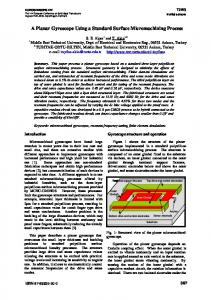
Many micromachined capacitive gyroscopes have been reported [1][2][3][4], where many of them require either vacuum packaging or multi-chip assembly. An integrated gyroscope has possible advantages such as lower cost and higher sensitivity due to less parasitic capacitance. Post CMOS micromachining [5] enables the integration of circuits and mechanical sensors on a single chip. A CMOSMEMS Z-axis gyroscope fabricated in this process with a conventional aluminum CMOS chip has been reported in [6]. The drawback of the Al version is that the device suffers severe out-of-plane curl because of large stress in the multi-layer structure. Potential improvement methods include using low stress material and thicker layers, which led to the investigation of using a six-layer Cu CMOS process. COPPER CMOS MICROMACHING PROCESS The gyroscope described in this paper combines highaspect-ratio CMOS micromachining technology [5] and the copper CMOS technology. It is fabricated in the UMC 0.18 µm six copper layer low-k CMOS digital process. The reason to choose the copper process includes a) the copper layer is plated at low temperature and it has lower stress, b) six combined copper and dielectric layers provide thick structures (8 µm Cu vs. 5 µm Al). Compared to three layers in the aluminum version, the CMP copper process is more uniform and is expected to have less curl. Other benefits from the copper process include higher mass density
0-7803-7185-2/02/$10.00 ©2002 IEEE
released microstructure
stator
(c)
exposed silicon
Figure 1: Copper CMOS-MEMS process. (a) CMOS chip after fabrication (b) anisotropic RIE removes dielectric (c) isotropic RIE undercuts silicon substrate (8.96 g/cm3 Cu vs. 2.7 g/cm3 Al) and low-k oxide. The mass is critical for inertial sensing as it directly limits the acceleration noise floor. The low-k process results in lower parasitic capacitance and thus has higher sensitivity when on-chip capacitance sensing technology is employed. The layout of circuits with micro-structure patterning in the metal layers is sent out for copper chip fabrication. Figure 1(a) shows the cross section of the chip after copper CMOS fabrication. After the foundry fabrication, two dry etch steps, similar to the aluminum CMOS-MEMS process [5], are used to define and release the mechanical structure. In the first step of post CMOS processing (Figure 1(b)),
631
dielectric layers are removed by an anisotropic CHF3/O2 reactive ion etch (RIE) with the top copper layer acting as an etch resistant mask. In the next step, an isotropic SF6/O2 RIE is then performed to etch away the bulk silicon and release the structure (Figure 1(c)). Multi-layer conductors can be built in the composite structure, which gives flexible designs which require multiple signals. Due to different properties of the copper chip, the old aluminum releasing process[5] is tuned to fit the copper version [7] (Plasma Therm 790 chamber, 80 W, CHF3 25 sccm, O2 22.5 sccm, 60 mtorr, DC bias 350 V, etching time 350 min). The released copper structures show some different properties from Al structures. First, the copper will suffer corrosion when exposed to moisture in the air. The structures are easy to stick together and difficult to pull them apart electrostatically. So contact must be avoided by stoppers.
generates the electrostatic force for vibration, while the comb fingers on the opposite side sense the movement of the vibrating frame to sustain the oscillation. The accelerometer is a fully differential with sensing fingers attached at the inner rigid frame. Since the copper gyroscope is expected to have much lower curl, the outer curl matching frame is no longer necessary. The outer driving comb fingers are directly anchored on the substrate. One more benefit of this change is that it decreases the routing path from the sensor to the circuits and thus parasitic capacitance is decreased. Table 1 summarizes some design parameters and comparison between the copper and aluminum gyroscope. Table 1. Design parameter comparison between copper and aluminum gyro
Copper
GYROSCOPE STRUCTURE DESIGN The schematic view of the gyroscope is shown in Figure 2. substrate anchor
driving fingers
x motion
Ω
transducer size
330 µm × 410 µm 360 µm × 500 µm
layer used
6 layer of copper
structure thickness 8 µm
vibrating frame
y
finger spring
a
Vm-
proof mass
Vm+
Vs+
Vm+ Vs+ Vs -
3 layer of aluminum 5 µm
sense comb fingers
85 µm× 4 µm × 40
61.5 µm× 3.9 µm × 40
drive comb fingers
7.8 µm× 2.4 µm × 27
11.4 µm× 2.7 µm × 23
driving mode spring
88 µm× 1.8 µm × 1 turn
105 µm× 1.8 µm × 1 turn
sensing mode spring
102 µm× 1.8 µm × 1 turn
128 µm× 1.8 µm × 1 turn
rigid frame, anchor
Vs-
Aluminum
driving mode reso- 8.8 kHz nant frequency
9.02 kHz
sensing mode reso- 9.0 kHz nant frequency
11.0 kHz
Vm-
INTERFACE DESIGN nested accelerometer
oscillation sensing fingers
accelerometer sense fingers
Figure 2: Schematic of gyroscope and inner sensing equivalent model. The gyroscope is composed of an accelerometer nested in a movable rigid frame, which is identical to the topology in [6]. An outer actuator drives the rigid frame in one lateral direction (X-axis), and the inner accelerometer measures the orthogonal deflection due to the Coriolis force (Y-axis). The elastically gimbaled structure completely decouples the Coriolis sense mode from the vibration drive mode[4]. The modulation clock and sensing signals of the inner accelerometer are routed through the multi-layer springs. One set of comb fingers on the outer rigid frame
0-7803-7185-2/02/$10.00 ©2002 IEEE
An on-chip unity gain sensing buffer detects the capacitance change due to deflection of comb fingers (Figure 3). The biasing problem of the capacitive sensing interface is solved by using a small transistor (W/L=2µm/2µm) working in the subthreshold range with diode connection between the gate and drain of the input transistor. It exhibits large resistance. This technique eliminates the requirement of large resistors which have relatively large capacitance in the CMOS process. To avoid the damage caused by undercut of silicon in the RIE (see Figure 1 (c)), circuits are put 40µm away from the edge of the sensor’s etch pit. Except for the microstructure, the whole chip area is covered by the top metal layer. The block diagram of the gyroscope system is shown in Figure 4.
632
Vm+
substrate
proof mass sensing spring sensing fingers
Vm64/1.2
45/0.9
Vdd (3V) 2/2
out
in 20/0.9 72/1.2
bias
28/1.2
Figure 3: Capacitive sensing interface driving mode
x y
Ω
sensing mode accelerometer sensing
Vm+
integrated on chip driving spring vibrating frame LPF1
Vm-
1
driving fingers
Figure 5: Micro-picture of a copper gyroscope.
2 Vm+ Vm-
oscillation sensing 3
oscillation driving amp LPF2 4
(a)
Figure 4: Block diagram of gyroscope system. EXPERIMENTS Figure 5 shows an optical microscopic image of the released gyroscope. Optical profilemeter measuremensts of the copper gyroscope and its aluminum counterpart are shown in Figure 6. As expected, the copper structure has much less curl than the aluminum version (maximum vertical curl: Cu 2 µm vs. Al 12 µm). In the dynamic test, the three-axis motion of the dithered proof mass in driving mode (Figure 7) is measured by sweeping the frequency response with an applied voltage on the actuator (5 VDC + 5 VAC). As can be seen, there is no substantial coupling between the driving mode (X-axis) and sensing mode (Y-axis). The out-of-plane motion (Z-axis) is also significantly reduced compared to [6]. Figure 8 shows the sensing mode response to an applied 1G 100 Hz accel-
0-7803-7185-2/02/$10.00 ©2002 IEEE
(b) Figure 6: Curl comparison. (a) Aluminum gyroscope. (b) Copper gyroscope.
633
250 kHz carrier 100 Hz acceleration
Figure 8: Sensing mode response to 1G 100Hz acceleration. Figure 7: Gyro proof-mass three axis motion in driving mode. eration in the sensing axis (Y-axis). The rotation test on a rate table shows that the sensor has a sensitivity of 0.8 µV/ °/sec and noise floor of 0.5°/sec/ Hz . This number is not an improvement from its aluminum counterpart. The possible explanation include a) even though the copper is heavier than the aluminum, as can bee seen from the Table1, the copper gyroscope is smaller than the aluminum one and they have similar resonant frequency which means they have similar physical noise limit. b) the copper version uses a unity gain buffer as sensing interface while putting higher gain at the front stage (Al version) is helpful to decrease the whole system noise. The maximum long period drift is 12° over a 24 hr period. CONCLUSION We have reported a CMOS-MEMS gyroscope fabricated in commercial copper CMOS process. Compared to the aluminum process, the copper structures suffer much less curl, which enables design of much larger and more complicated devices to enhance the performance. ACKNOWLEDGMENT This device is a side-product of a prize winning project in the SRC copper design challenge competition held in 2000. The authors would like to thank the Semiconductor Research Corporation (SRC), UMC, Novellus and SpeedFam-IPEC for funding this competition and help in the fabrication. This work was partially sponsored by DARPA under agreement F30602-97-2-0323.
0-7803-7185-2/02/$10.00 ©2002 IEEE
REFERENCES [1] W. A. Clark, R. T. Howe, “Surface micromachined Zaxis vibratory rate gyroscope,” Solid state Sensor and Actuator workshop ‘96 pp. 283-287, Hilton Head, SC [2] S.S. Beak, Y.S. Oh, B.J. Ha, S. D. An, B.H. An. Song, C.M. Song, “Asymmetrical Z-axis gyroscope with a high aspect ratio using simple and new process,” MEMS 99, pp. 612-617 [3] W. Geiger, B. Folkmer, J. Merz, H. Sandmaier, and W. Lang, “A new silicon rate gyroscope,” MEMS 98, Heidelberg, Germany, Feb. 1998, pp. 615-620 [4] M. S. Kranz and G. K. Fedder, "Micromechanical Vibratory Rate Gyroscopes Fabricated in Conventional CMOS," Proc. Symposium Gyro Technology, Stuttgart, Germany, September 16, 1997, pp. 3.0-3.8. [5] G.K.Fedder, S.Santhanam, M.L.Reed, S.C.Eagle, D.F.Guillou, M.S.-C.Lu, and L.R.Carley, “Laminated high-aspect-ratio micro-structures in a conventional CMOS process,” Sensors and Actuators, v.A57, no. 2, pp. 103-110. [6] Hao Luo, G.K. Fedder, L.R.Carley, “An Elastically Gimbaled Z-axis CMOS-MEMS Gyroscope,” International Symposium on Smart Structures and Microsystems 2000, HongKong, Oct. 19-21, B1-2, pp1~6. [7] X. Zhu, S. Santhanam, H, Lakdawala, H. Luo and G. K. Fedder, "Copper Interconnect Low-K Dielectric Post-CMOS Micromaching," The 11th International Conference on Solid-State Sensors and Actuators (Tansducers’01), Munich, Germany, June 10-14, 2001. pp. 1548~1551.
634