sensors Article
A Practical and Portable Solids-State Electronic Terahertz Imaging System Ken Smart 1 , Jia Du 1, *, Li Li 1 , David Wang 1 , Keith Leslie 1 , Fan Ji 2 , Xiang Dong Li 2 and Da Zhang Zeng 2 1
2
*
Commonwealth Scientific and Industrial Research Organisation (CSIRO), Lindfield, NSW 2070, Australia;
[email protected] (K.S.);
[email protected] (L.L.);
[email protected] (D.W.);
[email protected] (K.L.) Chengdu Shuguang Optical Fiber Network Co., Ltd, 56, Tianhui Mid-street, Hi-Tech Zone, Chengdu 610041, Sichuan, China;
[email protected] (F.J.);
[email protected] (X.D.L.);
[email protected] (D.Z.Z.) Correspondence:
[email protected]; Tel.: +61-2-9413-7107
Academic Editors: Vincenzo Spagnolo and Wilmar Hernandez Received: 21 December 2015; Accepted: 19 April 2016; Published: 22 April 2016
Abstract: A practical compact solid-state terahertz imaging system is presented. Various beam guiding architectures were explored and hardware performance assessed to improve its compactness, robustness, multi-functionality and simplicity of operation. The system performance in terms of image resolution, signal-to-noise ratio, the electronic signal modulation versus optical chopper, is evaluated and discussed. The system can be conveniently switched between transmission and reflection mode according to the application. A range of imaging application scenarios was explored and images of high visual quality were obtained in both transmission and reflection mode. Keywords: terahertz; imaging; solid-state electronic components
1. Introduction Terahertz (THz) radiation, in between the millimeter-wave (100 GHz) and far infra-red (10 THz) regions of the electromagnetic spectrum, displays many unique properties, such as a strong sensitivity to polar liquids [1], high transmission through a range of non-conducting materials [2,3], and spectroscopic responses to many materials [4]. These features can be applied to medical imaging and diagnosis (for example, detecting skin cancers beneath the skin due to increased water content in tumour cells [5]), remote detection of explosive substances and drugs through spectroscopic response of crystalline compounds [3,6], and non-destructive imaging of items concealed in optically opaque packaging [2,3,7]. Recent research and achievements in THz technology are summarized in a number of review papers [4,7,8]. Since THz imaging was first demonstrated in the mid-90s [9], various technologies have been explored for this application over the past two decades. Different system architectures were built depending on what types of sources, detectors and other components were accessible. For example, typical optical-approached systems are based on various laser sources (femtosecond optical pulses, semiconductor lasers, and quantum cascade lasers) to generate and tune THz signals and photoconductive or photosensitive materials to detect/receive the signals. Time domain spectroscopic imaging and monochromatic imaging (continuous-wave (CW) imaging) [4,6,9,10] have been recognized as promising methods, especially for non-destructive inspection and materials analysis. Solid-state electronic component-based imaging systems have also been developed based on various microwave electronic components. Virginia Diodes Inc. (Charlottesville, VA, USA; http://vadiodes.com) has now offered a range of relatively mature and compact THz products such as amplifier multiplier chain THz sources and diode detectors enabling potentially compact
Sensors 2016, 16, 579; doi:10.3390/s16040579
www.mdpi.com/journal/sensors
Sensors 2016, 16, 579
2 of 12
high-performance all-electronics systems. These electronic THz imaging systems, typically in sub-THz frequency ranges, are promising for variety practical applications (for example [11]). Optic scheme is commonly used to direct and couple the THz signal to the specimen and the detector [11–13]. Since the solid-state electronic devices are fabricated by planar micro-lithographic processing techniques, they can be easily scaled up to large array devices for multi-pixel imaging. It is not however the purpose of this paper to provide an extensive overview of various imaging technologies, and reference [7] gives a good summary and comparison of a range of imaging technologies. Until recent advances in THz sources and detectors, there has been a lack of low cost commercial high-performance THz instruments. Most of the THz systems presented in the literature are laboratory bench-top demonstrators; complex, bulky, difficult to operate and impossible to move. For wide adoption of THz technology to occur, the systems will have to become more compact, affordable and user friendly, which requires new approaches to many details of the components and system architectures. Some recent progress in emerging commercial THz instruments is worth mentioning. For example, Lake Shore Cryotronics, Inc. (Westerville, OH, USA; www.lakeshore.com) and QMC Instruments Ltd. (Billingshurst, UK; www.terahertz.co.uk/qmc) have offered cryogenically cooled THz spectrometers for materials characterisation, but the instruments are still bulky and expensive. Advantest Co. (Tokyo, Japan; www.advantest.com) offers a series of spectroscopic analysis systems. TeraSense Group (San Jose, CA, USA; www.terasense.com) has presented a number of THz spectroscopy systems and very recently the sub-THz imaging camera. Despite this progress, available commercial high-performance and low cost THz systems, especially imaging systems (available commercial systems are mostly spectroscopy systems), are still scarce and high cost, preventing widespread use of THz technology. Continuing research and development of THz instruments is anticipated to further drive the system costs down and promote application of the THz technology. CSIRO has in recent years developed electronic component-based THz imaging systems [12,13], antenna-coupled integrated THz detectors [14] and sensitive superconducting detectors [15–17]. The previous imaging system, though producing excellent images, employed a large size backward-wave oscillator (BWO) THz source and a series of more expensive and harder to align optical mirrors to form a quasi-optical active imaging system. The system was too bulky and complicated to operate. The motivation of this work was to develop a more compact, lower cost, user-friendly and industry-adaptable imaging system. We have employed more compact state-of-the art solid-state THz components, explored various beam guiding architectures and have built a practical and simpler imaging system that could be readily applied to imaging in either transmission or reflection mode according to the desired application. 2. Experimental Setup—Hardware and System Configurations Moving to a more compact system, we have first made various changes to the hardware components. The previous BWO THz source was replaced with a much more compact state-of-the art solid-state 625 GHz Amplifier/Multiplier chain (AMC) from Virginia Diodes Inc. It generates CW radiation between 590 and 650 GHz with a maximum output of around 1 mW. While the output power is less than that produced by the BWO (10 mW maximum), certain limitations of the BWO such as a finite lifespan of approximately 1000 h are overcome. The BWO has a nonstandard size output waveguide close to WR10 leading to the guide being overmoded at the test frequencies, which results in a non-ideal amplitude distribution across the collimated beam (see Figure 9a in [18]). The new solid-state AMC source does not have this overmoding issue as it has appropriately sized WR1.5 waveguide and diagonal waveguide horn with approximately 25 dB of gain. The source is also frequency sweepable and comes with a TTL modulation port. A compact economy synthesizer, instead of a standalone bench top RF signal generator, was used to supply the input signal for the AMC THz source and it offers digital tuning via LabVIEW by the system control computer. The AMC and compact synthesizer represent a great advantage over both the size, weight and complexity of the previous BWO system.
Sensors 2016, 16, 579
3 of 12
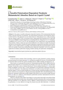
Virginia Diodes WR-1.5ZBD Zero-bias Schottky diode detectors were used to receive the transmitted or reflected signals from the sample. The detectors were mounted on a precision XY translation mounts allowing for fine adjustment of detector to optical lens alignment. The XY translator 2016, 16, 579 3 of 11 providesSensors ˘2 mm of travel perpendicular to the optical axis. The THz imager is a quasi-optical active imaging comprising andthe focusing Virginia Diodes WR-1.5ZBD Zero-bias Schottky system diode detectors were collimating used to receive mirrors.transmitted Mirrors were used to signals focus the THz onto samplewere andmounted then onto detector.XY Precision or reflected from thebeam sample. Thethe detectors onthe a precision translation allowingoffor fine aligned adjustment of detector to optical alignment.the Thebeam XY signal lens alignment andmounts maintenance these lenses are important forlens maximizing translator provides ±2 mm of travelthe perpendicular to the opticalOff-axis axis. or signal-to-noise ratio thus obtaining best quality images. parabolic mirrors were used in The THz imager is a quasi-optical active imaging system comprising collimating and focusing our earlier imaging system [12–16]. They proved difficult and time consuming to align and realign mirrors. Mirrors were used to focus the THz beam onto the sample and then onto the detector. after any movement or relocation or change of system configuration for different measurements. The Precision lens alignment and maintenance of these aligned lenses are important for maximizing the off-axis beam parabolic mirrors were replaced plano-convex Teflon PTFE lenses in ourmirrors current new signal or signal-to-noise ratio thuswith obtaining the best quality images. Off-axis parabolic system which employed a linear arrangement of the lenses. The PTFE and lenses the benefits were used in our earlier imaging system [12–16]. They proved difficult timeoffer consuming to alignof easier and and realign anyextent movement relocation or 10% change for optical differentmirrors. alignment to aafter lesser lowerorcost, at only of of thesystem cost ofconfiguration the parabolic measurements. The off-axis parabolic mirrors were replaced with plano-convex Teflon PTFE lenses Experiments were carried out to compare both types of lenses and the beam alignment schemes. We in our current new system which employed a linear arrangement of the lenses. The PTFE lenses offer obtained similar detectable signal amplitude and signal-to-noise ratio (SNR) from both. Although the the benefits of easier alignment and to a lesser extent lower cost, at only 10% of the cost of the PTFE lenses have higher lossExperiments than that ofwere thecarried off-axis a simpler better alignment parabolic optical mirrors. outmirrors, to compare both typesand of lenses andbeam the beam compensated the loss. One disadvantage of the PTFE lenses over the mirrors is that visible light does alignment schemes. We obtained similar detectable signal amplitude and signal-to-noise ratio (SNR) not go through therefore cannot behave used for coarse alignment. This disadvantage was partially from both.and Although the PTFE lenses higher loss than that of the off-axis mirrors, a simpler and better beam alignment compensated the loss. One disadvantage of the PTFE lenses over the mirrors fixed in our system as described in next section by locking in all the lenses (and the detector) in is that light removed does not gothe through thereforealignment cannot be used coarse the same axis,visible and thus need and for coarse (onlyforthe focalalignment. distanceThis needs fine disadvantage was partially fixed in our system as described in next section by locking in all the lenses adjustment which can be monitored with the detector signal level). (and the detector) in the same axis, and thus removed the need for coarse alignment (only the focal Figure 1 shows the adjustment exampleswhich of our quasi-optical transmission system improvement distance needs fine can be monitored with the detectorimaging signal level). process. TheFigure left photograph is our earlier system using the BWO source and theimprovement off-axis parabolic 1 shows the examples of our quasi-optical transmission imaging system process. The left photograph is our earlier system using the BWO source and the off-axis parabolic mirrors. The middle picture shows a linear lens alignment scheme using the plano-convex PTFE lenses mirrors. The middle picture shows a linear lens alignment scheme using the plano-convex for testing the beam alignment and the image quality. The picture on the right showsPTFE the further lenses for testing the beam alignment and the image quality. The picture on the right shows the improvement by locking in all the lenses in the same axis, i.e., reducing the freedom of the movement of further improvement by locking in all the lenses in the same axis, i.e., reducing the freedom of the individual lens using a in-house fabricated PVC circular cover. Changing from the off-axis alignment movement of individual lens using a in-house fabricated PVC circular cover. Changing from the to the linear system hastosignificantly simplified the system and reduced the time required to realign off-axis alignment the linear system has significantly simplified the system and reduced the time the beam after the system the configuration changed. being changed. required to realign thebeing beam moved after the or system being moved or being the configuration
Figure 1. Examples of the system improvement steps with varied hardware and the beam guiding schemes.
Figure 1. Examples of the system improvement steps with varied hardware and the beam guidingFigure schemes. 2 shows the final imaging system mounted on a portable plate without the cover. It employs a lens cage-system to lock the linear-aligned lens and is switchable between transmission and reflection mode. We also designed a removableon beam splitter fitted intowithout a lens mounting Figure 2 showsimaging the final imaging system mounted a portable plate the cover. It cube (see Figure 2 inset) as part of the lens alignment system so the system can be easily switched employs a lens cage-system to lock the linear-aligned lens and is switchable between transmission from the transmission to a reflection mode. The beam splitter consists of a high resistivity float zone and reflection imaging mode. We also designed a removable beam splitter fitted into a lens mounting 0.5 mm thick silicon wafer. High resistive silicon is one of the only isotropic crystalline materials with cube (see Figure 2 inset) part ofmaintaining the lens alignment system so the system can and be easily switched a wide bandwidth of as operation, up to 50%–54% transmission at millimetre terahertz from thewaves. transmission to aimaging reflection mode. The beam splitter consists high resistivity float zone The complete system hardware is shown in Figure 2 fromof lefta to right; source, beam
0.5 mm thick silicon wafer. High resistive silicon is one of the only isotropic crystalline materials with a wide bandwidth of operation, maintaining up to 50%–54% transmission at millimetre and terahertz
Sensors 2016, 16, 579 Sensors 2016, 16, 579
4 of 12 4 of 11
splitter The mount (cube),imaging reflection modehardware detector in a mount to the transmission path, waves. complete system is shown in perpendicular Figure 2 from left to right; source, beam Sensors 2016, 16, 579 4 of 11 the frequency abovemode the detector, focusing lenses, XY sample path, scanner, splitter mountsynthesizer (cube), reflection detectorcollimation in a mountand perpendicular to thethe transmission the splitter mount (cube), reflection mode detector in a mount perpendicular to the transmission path, and the transmission mounted in a precision XY translation frequency synthesizermode abovedetector the detector, collimation and focusing lenses, themount. XY sample scanner, and the frequency synthesizer above the detector, collimationXY andtranslation focusing lenses, the XY sample scanner, the transmission mode detector mounted in a precision mount. and the transmission mode detector mounted in a precision XY translation mount.
Figure 2. A view of the full system mounted on a portable optical plate (450 mm × 750 mm) showing
Figure 2. A viewaligned of the full system mounted on a portable optical plate (450 mm ˆ 750 mm)for showing a linearly source-lenses-sample-detector scheme and a removable beam splitter (inset) Figure 2. A view of the full system mounted on a portable optical plate (450 mm × 750 mm) showing a linearly aligned source-lenses-sample-detector scheme and a removable beam splitter (inset) for changing between transmission and reflection mode. a linearly aligned source-lenses-sample-detector scheme and a removable beam splitter (inset) for changing between transmission and reflection mode. changing between transmission and reflection mode. The operation schematic diagram is shown in Figure 3 which illustrates how the current THz imaging system is configured. As discussed the system employs a caged lens-mounting set-up where
Thetheoperation operation schematic diagram is shown shown Figure how the THz plano-convex PTFE lenses are mounted in in aincage system formedillustrates by parallelhow rods.the Thecurrent cage The schematic diagram is Figure 33 which which illustrates current THz imagingmounting system is is configured. Asadiscussed discussed the system employs caged lens-mounting set-up where where locks all lenses on single axis the thussystem reducing the freedom of individual lens movement imaging system configured. As employs aa caged lens-mounting set-up and achievingPTFE the best lens alignment. The rigid mounting simplifies theby alignment of the source the plano-convex lenses are in aa cage system formed parallel rods. The cage the plano-convex PTFE lenses are mounted mounted in lens cage system formed by parallel rods. The cage beam to sample and then to detector and produce more robust imaging system. The system can now mounting locks all lenses on a single axis thus reducing the freedom of individual lens movement mounting locks all lenses on a single axis thus reducing the freedom of individual lens movement be moved and realigned in a matter of minutes if need be. The advantages of using such a rigid cage and achieving achieving the the best best lens lens alignment. alignment. The The rigid rigid lens lens mounting mounting simplifies simplifies the the alignment alignment of of the source source and mounting scheme have also been recognised by Hoyer et al. [19] in their portable THz scanner the for beam to sample and then to detector and produce more robust imaging system. The system can now beam tostructural sample and then to detector and produce more robust imaging system. The system can now inspection of buildings. be moved and realigned in a matter of minutes if need be. The advantages of using such a rigid cage be moved and realigned in a matter of minutes if need be. The advantages of using such a rigid cage mounting scheme scheme have have also also been been recognised recognised by by Hoyer Hoyer et et al. al. [19] [19] in in their for mounting their portable portable THz THz scanner scanner for structural inspection of buildings. structural inspection of buildings.
Figure 3. Schematic of the quasi-optical THz transmission and reflection imaging system.
Figure imaging system. system. Figure 3. 3. Schematic Schematic of of the the quasi-optical quasi-optical THz THz transmission transmission and and reflection reflection imaging
Sensors 2016, 16, 579
5 of 12
3. Results and Discussion 3.1. Image Scanning and Resolution An image of the measured transmission or reflection properties of the sample is generated by raster scanning the sample through the fixed focused point as illustrated in Figure 3. The THz signal generated by the AMC is collimated and focused onto the sample and then the transmitted or reflected signal is collected and focused on the detector by another pair of lenses. The sample is mounted and scanned in the X and Y planes with two moving linear translation stages. A lock-in amplifier synchronized with an optical chopper (set at 1 kHz speed) is used to acquire the detector voltage responses, which are processed by a computer to produce an image using an in-house developed LabVIEW (http://wwwni.com/labview) program. The resolution of the system is determined by the spot size of the beam on the sample. The collimation and focusing lenses help in maximizing the beam strength from the source and minimizing the spot size on the sample. The theoretical spatial resolution can be estimated using the Rayleigh criterion ∆x = 1.22 λf/D assuming the perfect optical alignment, where the wavelength λ = 3 ˆ 108 ms´1 /614 GHz = 488 µm, f and D are the focal length and diameter of the focusing lenses. A THz signal of 614 GHz was used in the experimental results. The estimated theoretical spatial resolution is 1.19 mm. In the experiments, compromise must be made between the resolution and total scanning time. For the images shown in this paper, a typical resolution of 0.5 mm was used for a scanning area of 50 mm ˆ 50 mm which gave an image size of 100 ˆ 100 or 10,000 pixels. It took about 10 min to obtain the images. We examined the experimental resolution of our imaging system by plotting out 1D line scans of the image data corresponding to the image shown in Figure 4. Figure 4 is a transmission THz image of a computer floppy disk (Figure 4a) showing sharp metal edges obtained with above mentioned scanning conditions and a photograph (Figure 4b) showing the floppy disk; flipped to correspond to scanned image as the data is received on the rear of the sample. The signals blocked by the metallic parts are shown as blue colour in image (Figure 4) and correspond to zero signal level in single line scans (Figure 5). The maximum transmitted signal is shown in red colour in the image. Note that the blue section on right side was caused when the signal was blocked by a metal sample holder. Sensors 2016, 16, 579
6 of 11
(a)
(b)
Figure 4. (a) A transmission image of a computer floppy disk; a scanned area of 50 mm × 50 mm at a Figure 4. (a) A transmission image of a computer floppy disk; a scanned area of 50 mm ˆ 50 mm at a resolution of 0.5 mm. The black lines indicate the single line scans at vertical line 17 and horizontal resolution of 0.5 mm. The black lines indicate the single line scans at vertical line 17 and horizontal line 23; (b) is the photograph of the floppy disk flipped to correspond to scanned image. line 23; (b) is the photograph of the floppy disk flipped to correspond to scanned image.
(a)
(b)
Figure 4. (a) A transmission image of a computer floppy disk; a scanned area of 50 mm × 50 mm at a Sensors 2016,resolution 16, 579 of 0.5 mm. The black lines indicate the single line scans at vertical line 17 and horizontal line 23; (b) is the photograph of the floppy disk flipped to correspond to scanned image.
6 of 12
(a)
(b) Figure 5. Line scans of the image data: the detected signal level of the transmitted THz beam versus
Figure 5. Line scans of the image data: the detected signal level of the transmitted THz beam versus the the pixel point (upper x-axis) and spatial position (lower x-axis). (a) corresponds to the single line pixel scans pointat(upper spatial position (lower x-axis). (a) corresponds to the single line verticalx-axis) line 17 and in Figure 4a and (b) corresponds to the horizontal line 23 shown in Figure 4a.scans at vertical line 17 in Figure (b)pixel corresponds theeach horizontal line 23 shown in Figure the 4a. The The upper x axis shows 4a theand image points (0.5tomm step) and lower axis is converted upperposition x axis shows the image pixel points (0.5 mm each step) and lower axis is converted the position points in both figures. points in both figures.
The black lines indicate the single line scans at vertical line 17 and horizontal line 23 shown in Figure 5. The imaging system scans in the vertical Y plane and steps in the horizontal X plane to build an image. A slight blurring at the metal edges is visible, which is caused by the scattering effect of the metal edge. This effect is minimised in our system due to the focusing effect of the convex lens; only one point of ~1 mm (theoretic prediction is 1.19 mm) in diameter is exposed to the beam and measured by the device. Therefore although the metal edges still scatter the beam this only causes slight signal dilution (green colour regions adjacent to the blue colour edges). From the image in Figure 4, the visible blurred regions (green colour) along the metal edges (vertical or horizontal edges) are approximately 2 pixels, i.e., around 1 mm. The single line scans in Figure 5 correspond to the vertical line 17 across the rectangular shape metallic frame on the left side of the image and the horizontal line 23 across the small hole in the circular centre of the metallic part shown in Figure 4. The THz beam signal is completely blocked by the metallic parts resulting in zero signal level (blue in the image) and reaches the maximum signal level (red in the image) in the plastic parts of the disk which are more transparent to the THz beam. The marked widths in the line scans shown in Figure 5 show good agreement with the dimension-marked parts in Figure 4 photograph (red arrows). It can be seen that 10%–90% rise in the transmitted signal level occurs between 1.0 and 1.5 mm transition at each sharp metal edge, consistent with the visual colour change region (green) in the image (Figure 4). This provides a measure for the spatial resolution of our imaging system. The experimental results showed that our system has diffraction-limited resolution close to the theoretical spatial resolution (~1.19 mm).
Sensors 2016, 16, 579
7 of 12
3.2. Imaging Results Sensors 2016, 16, 579 in Reflection Mode
7 of 11
Reflection mode is suitable for many practical applications, such as security screening and 3.2. Imaging Results in Reflection Mode Sensors 2016, 16,testing 579 7 of 11 non-destructive in industrial environments [10]. Reflection mode is particularly useful where Reflection mode is suitable for many practical applications, such as security screening and nonthe sample is bulky and cannot be placed at transmission focal point or where the THz radiation cannot destructive environments [10]. Reflection mode is particularly useful where the 3.2. Imaging testing Results in industrial Reflection Mode penetrate or is largely attenuated through the sample to obtain enough signal level at the detector sample is bulky and cannot be placed at transmission focal point or where the THz radiation cannot Reflection mode is suitable for many practical applications, such security screeningsurfaces and non-or for for quality imaging. Reflection mode is also suitable for imaging ofashighly reflective penetrate or is largely attenuated through the sample to obtain enough signal level at the detector for destructive testing in industrial environments [10]. Reflection mode is particularly useful where the and imaging theimaging. surface features sub-surface interface of a sample; forreflective examplesurfaces the detection of rust quality Reflectionor mode is also suitable for imaging of highly or for imaging sample is bulky and cannot be placed at transmission focal point or where the THz radiation cannot corrosion underfeatures paint [12] and non-destructive testing for of valuable historical artefacts [20]. the surface or sub-surface interface of a sample; example the detectionor ofcultural rust and corrosion penetrate or is largely attenuated through the sample to obtain enough signal level at the detector for Figure 6 shows imaging of a 50 cent coin and a kangaroo key ring in the reflection under paint [12] and non-destructive testing of valuable historical or cultural artefacts [20]. mode where quality imaging. Reflection mode is also suitable for imaging of highly reflective surfaces or for imaging Figure was 6 shows imaging of a 50 coin and areflected kangaroofrom key ring the reflection where a beam splitter used to deflect thecent THz beam the in sample surfacemode to the detector the surface features or sub-surface interface of a sample; for example the detection of rust and corrosion a beam splitter was used to deflect the THz beamTHz reflected from the sample surface to the the detector perpendicular to the axis of the lens and original beam. The image obtained with reflected under paint [12] and non-destructive testing of valuable historical or cultural artefacts [20]. perpendicular to in thethe axisinset. of theItlens and shows originalthe THz beam. topography The image obtained with the THz beam is shown surface features of mode the reflected coin and the Figure 6 shows imaging of a clearly 50 cent coin and a kangaroo key ring in the reflection where THz beam is shown in the inset. It clearly shows the surface topography features of the coin and the key ring. a beam splitter was used to deflect the THz beam reflected from the sample surface to the detector key ring. perpendicular to the axis of the lens and original THz beam. The image obtained with the reflected THz beam is shown in the inset. It clearly shows the surface topography features of the coin and the key ring.
Figure 6. Imaging of a 50 cents coin and a Kangaroo key ring in a reflection mode (note that the
Figure 6. Imaging a 50 cents coin the andintroduction a Kangaroo ring mounted in a reflection mode (note experiment wasof carried out before of key the cube beam splitter shownthat in the experiment was carried out before the introduction of the cube mounted beam splitter shown in Figure 2). Figure 6. Imaging of a 50 cents coin and a Kangaroo key ring in a reflection mode (note that the Figure 2). experiment was carried out before the introduction of the cube mounted beam splitter shown in Figure 2).
Figure 7. Imaging in reflection mode, showing a hidden object in shoe lining.
Figure 7. Imaging in reflection mode, showing a hidden object in shoe lining.
Figure 7. Imaging in reflection mode, showing a hidden object in shoe lining.
Sensors 2016, 16, 579
8 of 12
THz imaging has been explored for security applications such as detection of concealed weapon Sensors 2016, 16, 579 8 of 11 or dangerous objects due to its ability to penetrate through clothes and packaging materials [2,3]. Figure 7 shows another example measurement of a hidden object in a shoe using the reflection mode. THz imaging has been explored for security applications such as detection of concealed weapon The or main photograph shows theitssetup with the shoe mounted on the and XY scanner. The top inset[2,3]. shows dangerous objects due to ability to penetrate through clothes packaging materials a visual image of the hidden object, a scalpel inside the shoe lining material, and the lower inset shows Figure 7 shows another example measurement of a hidden object in a shoe using the reflection mode. the terahertz image of the hidden object. In the terahertz image blue The main photograph shows the setup with the shoe mounted on the XYcorresponds scanner. Theto topweak inset reflection shows of the THz waves and red shows strong reflection. The hidden object is clearly visible in theinset image a visual image of the hidden object, a scalpel inside the shoe lining material, and the lower demonstrating the ability of THz wave to penetrate common non-metallic materials such asto theweak canvas shows the terahertz image of the hidden object. In the terahertz image blue corresponds theshoe. THz The waves andindicates red shows strong reflection. The hidden object clearly applications, visible in clothreflection lining ofofthe result the suitability of our THz imager for is security the ability THz wave to penetrate common non-metallic materials such suchthe asimage a shoedemonstrating scanner in airports, for of example. as the canvas cloth lining of the shoe. The result indicates the suitability of our THz imager for
3.3. security Imagingapplications, Results in Transmission Mode such as a shoe scanner in airports, for example. Imaging in transmission mode can be used for applications such as non-destructive testing of or 3.3. Imaging Results in Transmission Mode inspection through opaque materials, including determining the fibre density or consistency of papers Imagingthe in transmission can be used applications such as non-destructive of or and cardboard, detection ofmode contaminants orfor inclusions in plastics and polymers.testing Transmission inspection through opaque materials, including determining the fibre density or consistency of mode can also be used to quantify the water content taking advantage of terahertz frequencies’ papers and cardboard, the detection of contaminants or inclusions in plastics and polymers. sensitivity to water and other polar liquids. It offers a non-contact method of monitoring water content Transmission mode can also be used to quantify the water content taking advantage of terahertz and distribution in both living things such as plants and non-living things such as wood polymers or frequencies’ sensitivity to water and other polar liquids. It offers a non-contact method of monitoring paper [21]. water content and distribution in both living things such as plants and non-living things such as Figure 8 shows example wood polymers or an paper [21]. measurement taken in transmission mode of a fresh leaf imaged at 614 GHz; the image clearly demonstrates keyinfeature of themode THz of radiation, i.e.imaged sensitivity Figure 8 shows an example measurementthe taken transmission a fresh leaf at to water. The THz image shows how the attenuation of the signal corresponds to water content 614 GHz; the image clearly demonstrates the key feature of the THz radiation, i.e. sensitivity to water. andThe distribution in the vein structure of the leaf, bothtolarge and fine and veindistribution structure can THz imageparticularly shows how the attenuation of the signal corresponds water content particularlyBlue in the vein structure of the bothabsorption large and fine structure canand be observed. be observed. colour represents theleaf, largest of vein the THz signal thus the Blue highest colour represents the largest absorption of the THz signal and thus the highest water content. water content. This presents a non-invasive way of monitoring water content and distributionThis within presentsstructures a non-invasive of monitoring content and distribution within structures biological such way as leaves. As the water measurement is non-contact it can biological be used on live plants as leaves. As the measurement is non-contact be used on live repeated in andsuch repeated in situations where observing changes itincan water content overplants time and are required. This situations where observing changes in water content over time are required. This example has further example has further implication for THz imaging being applied to medical imaging examinations, with implication for THz imaging being applied to medical imaging examinations, with potential potential applications in the areas of detection of skin and breast cancers or monitoring the hydration applications in the areas of detection of skin and breast cancers or monitoring the hydration of corneal of corneal grafts [5,22]. grafts [5,22].
(a)
(b)
Figure 8. Photograph (a) and the transmission THz image (b) of a fresh leaf.
Figure 8. Photograph (a) and the transmission THz image (b) of a fresh leaf.
3.4. TTL Electronic Modulation versus Optical Chopper
3.4. TTL Electronic Modulation versus Optical Chopper
The above results were obtained using an optical chopper to modulate the THz source signal at The above results using optical to modulate sourcetosignal the rate of 1 kHz. Thewere ACMobtained solid-state THz an source has achopper logic input that allowsthe the THz THz beam be TTL modulated up ACM to 5 kHz. This function allowshas further simplification of the THz system by to at the rate of 1 kHz.atThe solid-state THz source a logic input that allows the THz beam replacing the optical chopper withThis a small, low cost, logic signal simplification source. An experiment was system carried by be TTL modulated at up to 5 kHz. function allows further of the THz out to compare the system performance using the TTL electronic signal modulating the THz beam to replacing the optical chopper with a small, low cost, logic signal source. An experiment was carried that using the optical chopper modulation. Figure 9 compares the real-time detector voltage outputs
Sensors 2016, 16, 579
9 of 12
out to compare the system performance using the TTL electronic signal modulating the THz beam to that using optical Sensorsthe 2016, 16, 579 chopper modulation. Figure 9 compares the real-time detector voltage outputs 9 of 11 (note that a different detector was used in this measurement) acquired using both modulation methods (note rate that of a different detector was used in this measurement) acquired using both modulation at the same 1 kHz. The optical chopper modulated THz beam response shows some distortion methods at the same rate of 1 kHz. The optical chopper modulated THz beam response shows some due to the non-instantaneous nature of the optical chopping of the beam. In comparison, the TTL distortion due to the non-instantaneous nature of the optical chopping of the beam. In comparison, electronic signal modulated THz beam results in a near ideal response due to the fact that the electronic the TTL electronic signal modulated THz beam results in a near ideal response due to the fact that chopper can switch the RF power more quickly. The computer disk shown in Figure 4 was also imaged the electronic chopper can switch the RF power more quickly. The computer disk shown in Figure 4 using the modulation at the same speed, at 1 kHz, as that of the optical chopper, and the wasTTL also electronic imaged using the TTL electronic modulation the same speed, 1 kHz, as that of the optical result chopper, is shownand in the Figure 10. There are no observable differences in the visual quality of these two result is shown in Figure 10. There are no observable differences in the visual quality imagesof(Figures 4 and 10), leading us to the conclusion that it is possible to replace the function of these two images (Figures 4 and 10), leading us to the conclusion that it is possible to replace thethe the optical chopper with TTL logic signal without compromising the systemImplementation performance. opticalfunction chopperofwith TTL logic signal without compromising the system performance. Implementation of electronic provides us opportunity of developing a software-based of electronic modulation providesmodulation us an opportunity of an developing a software-based “virtual lock-in” “virtual lock-in” instead of the stand-alone analogue lock-in amplifier, willthe further amplifier instead of theamplifier stand-alone analogue lock-in amplifier, which will further which simplify system simplify the system and reduce the overall system cost. The development of a virtual lock-in amplifier and reduce the overall system cost. The development of a virtual lock-in amplifier and new signal and new signal processing method is underway. processing method is underway. Mechnical Optical Chopper
140
Signal VRF (mV)
120 100 80 60 40 20 0 0
1
2
3
4
Time (ms) (a) TTL Moduated THz Signal
140
Signal VRF (mV)
120 100 80 60 40 20 0 0
1
2
3
4
Time (ms) (b) Figure 9. Real-time detector voltage output VRF (t) traces of the modulated THz beam using a
Figure 9. Real-time detector voltage output VRF (t) traces of the modulated THz beam using a mechanical optical chopper (a) and an electronic signal via the TTL port on the AMC THz source (b). mechanical optical chopper (a) and an electronic signal via the TTL port on the AMC THz source (b).
Sensors 2016, 16, 579
10 of 12
Sensors 2016, 16, 579
10 of 11
Figure 10. The THz transmission image of the computer disk acquired using the TTL electronic signal Figure 10. The transmission computer disk acquired using the TTLused electronic signal4 modulation at THz the same chopperimage speedofofthe 1 kHz and scanning conditions as that in Figure modulation at the same chopper speed of 1 kHz and scanning conditions as that used in Figure 4 image image modulated with an optic chopper. modulated with an optic chopper.
The signal-to-noise ratio (SNR) can be estimated using the real-time voltage response VRF (t) The signal-to-noise (SNR) be the estimated usingis the real-time response VRF (t) amplitude divided by theratio noise floorcan when THz signal blocked. The voltage RMS noise voltage level amplitude divided by the noise floor the THz is blocked. noise voltage displayed on the lock-in amplifier withwhen the THz beamsignal blocked is 0.5 VThe (at RMS integration time of 5level ms) displayed on the lock-in theare THz beam blocked is ď0.5 µV time of (7265 5 ms) for both electronic and amplifier choppers with which believed to be limited by (at theintegration lock-in amplifier for both electronic and choppers which are believed to beTHz limited by the lock-in amplifier (7265level Lock-in Lock-in Amplifier, Signal Recovery). The detected beam signal voltage output in Amplifier, Signal Recovery). The~25 detected beam signal in transmission mode transmission mode is typically mV orTHz more (with the voltage chopperoutput “on” level but without the sample in is typically ~25a mV morethan (with50,000 the chopper butsystem. withoutThe the high sample in value place);results givingin a SNR place); giving SNRorbetter for our“on” current SNR high better 50,000 for our current system. The high SNR value results in high visual quality images. visual than quality images. 4. Conclusions 4. Conclusions A A practical practical and and portable portable solid-state solid-state electronic electronic component-based component-based THz THz imaging imaging system system was was presented in this work. More compact state-of-art solid-state THz components were employed and presented in this work. More compact state-of-art solid-state THz components were employed and various were explored explored to to improve improve its its performance, performance, compactness, compactness, portability portability and various system system configurations configurations were and simplicity simplicity to to operate. operate. The The system system can can be be conveniently conveniently switched switched between between transmission transmission and and reflection reflection mode mode to to suit suit different different application application scenarios. scenarios. The The optical optical configuration configuration has has resulted resulted in in good good spatial spatial resolution, resolution, similar similar to to the the theoretical theoretical value value of of ~1.2 ~1.2 mm mm at at operating operating frequency frequency of of 614 614 GHz. GHz. A A SNR SNR of of better than 50,000 was obtained. Images of high visual quality were obtained in both transmission and better than 50,000 was obtained. Images of high visual quality were obtained in both transmission and reflection samples. The imaging results demonstrated some key features of THz reflection mode modeon ona anumber numberofof samples. The imaging results demonstrated some key features of radiation including the penetration through non-conducting materialmaterial and sensitivity to waterto content, THz radiation including the penetration through non-conducting and sensitivity water which indicates its potential applications in security non-contact quality control the content, which indicates its potential applications in screening, security screening, non-contact qualityand control quantification of the water content in biological tissues. The easy-to-use and portable system is a major and the quantification of the water content in biological tissues. The easy-to-use and portable system step forward the industrial terahertzoftechnology. is a major steptowards forward towards the adoption industrialofadoption terahertz technology. Acknowledgments: Earlier contributions from CSIRO colleagues, Andrew Hellicar, Stephen Hanham and Acknowledgments: Earlier contributions from CSIRO colleagues, Andrew Hellicar, Stephen Hanham and Nasiha Nikolic, as well as the technical contributions to our current work by Ivan Kekic, are Nasiha Nikolic, as well as the technical contributions to our current work by Ivan Kekic, are gratefully gratefully acknowledged. acknowledged. Author Contributions: Ken Smart, Jia Du and Li Li conceived and designed experiments as well as performed many experiments; David Wang and Leslie provided some and electronic technical support; Fan Ji, Author Contributions: Ken Smart, JiaKeith Du and Li Li conceived andoptic designed experiments as well as performed Xiang Dong Li, andDavid Da Zhang Zeng application ideas experiments as the many experiments; Wang andcontributed Keith Leslieto provided some opticand andperformed electronic some technical support; Fan Ji, collaborators; Ken Smart and Jia Du wrote the paper. Xiang Dong Li, and Da Zhang Zeng contributed to application ideas and performed some experiments as the Conflicts of Interest: The and authors declare conflict collaborators; Ken Smart Jia Du wroteno the paper.of interest.
Conflicts of Interest: The authors declare no conflict of interest.
Sensors 2016, 16, 579
11 of 12
References 1. 2. 3. 4. 5.
6. 7. 8. 9. 10.
11. 12.
13.
14.
15. 16.
17.
18. 19.
20.
Kindt, J.T.; Schmuttenmaer, C.A. Far-Infrared Dielectric Properties of Polar Liquids Probed by Femtosecond Terahertz Pulse Spectroscopy. J. Phys. Chem. 1996, 100, 10373–10379. [CrossRef] Dickinson, J.C.; Goyette, T.M.; Gatesman, A.J.; Joseph, C.S.; Root, Z.G.; Giles, R.H.; Waldman, J.; Nixon, W.E. Terahertz imaging of subjects with concealed weapons. Proc. SPIE 2006, 6212. [CrossRef] Kemp, M.C.; Taday, P.F.; Cole, B.E.; Cluff, J.A.; Fitzgerald, A.J.; Tribe, W.R. Security applications of terahertz technology. Proc. SPIE 2003, 5070, 44–52. Ferguson, B.; Zhang, X.C. Materials for terahertz science and technology. Nat. Mater. 2002, 1, 26–33. [CrossRef] [PubMed] Woodward, R.M.; Cole, B.E.; Wallace, V.P.; Pye, R.J.; Arnone, D.D.; Linfield, E.H.; Pepper, M. Terahertz pulse imaging in reflection geometry of human skin cancer and skin tissue. Phys. Med. Biol. 2002, 47, 3853–3863. [CrossRef] [PubMed] Kawase, K.; Ogawa, Y.; Watanabe, Y.; Inoue, H. Non-destructive terahertz imaging of illicit drugs using spectral fingerprints. Opt. Express 2003, 11, 2549–2554. [CrossRef] [PubMed] Chan, W.L.; Deibel, J.; Mittleman, D.M. Imaging with terahertz radiation. Rep. Prog. Phys. 2007, 70, 1325–1379. [CrossRef] Tonouchi, M. Cutting-edge terahertz technology, Nature Photonics. Nat. Photonics 2007, 1, 97–105. [CrossRef] Hu, B.B.; Nuss, M.C. Imaging with terahertz waves. Opt. Lett. 1995, 20, 1716–1718. [CrossRef] [PubMed] Jansen, C.; Wietzke, S.; Peters, O.; Scheller, M.; Vieweg, N.; Salhi, M.; Krumbholz, N.; Jördens, C.; Hochrein, T.; Koch, M. Terahertz imaging: Applications and perspectives. Appl. Opt. 2010, 49, E48–E57. [CrossRef] [PubMed] Ok, G.; Choi, S.W.; Park, K.H.; Chun, H.S. Foreign Object Detection by Sub-Terahertz Quasi-Bessel Beam Imaging. Sensors 2013, 13, 71–85. [CrossRef] [PubMed] Hellicar, A.D.; Du, J.; Hanham, S.M.; Li, L.; Nikolic, N.; Li, Y.; Popescu, D. A 600 GHz imaging system for application exploration. In Proceedings of the 34th International Conference on Infrared, Millimeter, and Terahertz Waves, Busan, Korea, 21–25 September 2009; Volume 1–2, pp. 765–766. Hellicar, A.; Du, J.; Nikolic, N.; Li, L.; Greene, K.; Beeton, N.; Hanham, S.; Kot, J.; Hislop, G. Development of a Terahertz Imaging System. In Proceedings of the 2007 IEEE Antennas and Propagation Society International Symposium, Honolulu, HI, USA, 9–15 June 2007; pp. 5535–5538. Hellicar, A.D.; Hanham, S.M.; Hislop, G.; Du, J. Terahertz Imaging with Antenna Coupled Detectors. In Proceedings of the 3rd European Conference on Antennas and Propagation, Berlin, Germany, 23–27 March 2009; Volume 1–6, pp. 1575–1578. Du, J.; Hellicar, A.D.; Li, L.; Hanham, S.; Macfarlane, J.C.; Leslie, K.E.; Nikolic, N.; Foley, C.P.; Greene, K.J. Terahertz imaging at 77 K. Supercond. Sci. Technol. 2009, 22. [CrossRef] Du, J.; Hellicar, A.D.; Hanham, S.; Li, L.; Macfarlane, J.C.; Leslie, K.E.; Foley, C.P. Terahertz and millimetre wave imaging with a broadband Josephson detector working above 77 K. J. Infrared Millim. Terahertz Waves 2011, 32, 681–690. [CrossRef] Du, J.; Smart, K.W.; Li, L.; Leslie, K.E.; Hanham, S.M.; Wang, D.H.C.; Foley, C.P.; Ji, F.; Li, X.D.; Zeng, D.Z. A cryogen-free HTS Josephson junction detector for terahertz imaging. Supercond. Sci. Technol. 2015, 28. [CrossRef] Hislop, G.; Li, L.; Hellicar, A. Phase Retrieval for Millimeter-and Submillimeter-Wave Imaging. IEEE Trans. Antennas Propag. 2009. [CrossRef] Hoyer, T.; Loffler, T.; Saito, T.; Yukihira, N.; Deninger, A.; Fukunaga, K. A portable all-electronic THz scanner for the inspection of structural earthquake damage in Japanese buildings. In Proceedings of the 37th International Conference on Infrared, Millimeter, and Terahertz Waves, Wollongong, Australia, 23–28 September 2012; pp. 1–2. Fukunaga, K.; Picollo, M. Terahertz time domain spectroscopy and imaging applied to cultural heritage. In Proceedings of the 13th International Symposium on Nondestructive Characterization of Materials (NDCM-XIII), Le Mans, France, 20–24 May 2013.
Sensors 2016, 16, 579
21. 22.
12 of 12
Banerjee, D.; von Spiegel, W.; Thomson, M.; Schabel, S.; Roskos, H. Diagnosing water content in paper by terahertz radiation. Opt. Express 2008, 16, 9060–9066. [CrossRef] [PubMed] Bennett, D.B.; Taylor, Z.D.; Tewari, P.; Singh, R.S.; Culjat, M.O.; Grundfest, W.S.; Sassoon, D.J.; Johnson, R.D.; Hubschman, J.P.; Brown, E.R. Terahertz sensing in corneal tissues. J. Biomed. Opt. 2010, 16. [CrossRef] [PubMed] © 2016 by the authors; licensee MDPI, Basel, Switzerland. This article is an open access article distributed under the terms and conditions of the Creative Commons Attribution (CC-BY) license (http://creativecommons.org/licenses/by/4.0/).