Available online at www.sciencedirect.com
ScienceDirect Procedia Engineering 120 (2015) 1087 – 1090
EUROSENSORS 2015
Additive technologies for ceramic MEMS sensors A.A.Vasilieva,b*, A.V.Sokolova, A.V.Leginb, N.N.Samotaevc, K.Yu.Oblovc, V.P.Kimd, S.V.Tkachevd, S.P.Gubind, G.N.Potapove, Yu.V.Kokhtinae, A.V.Nisane a
National research center “Kurchatov Institute”, Moscow, Russia, Kurchatov sq., 1, Moscow, 123182,Russia b St. Petersburg ITMO University, Kronverkskiy pr. 49, 199034, St. Petersburg, Russia c National Research Nuclear University “MEPhI”, Kashirskoe chaussee, 31, 115409, Moscow, Russia d LLC AkKo Lab, Moscow, Russia e LLC Ostec, Moscow, Russia
Abstract The application of MEMS technology for the fabrication of MOX sensors with low power consumption becomes now a very important trend in gas sensor design. However, traditional silicon technology has some evident disadvantages, when applied in high-temperature devices produced in limited batch. We present our attempt to combine the advantages of ceramic MEMS technology (high working (600ºC) and technological treatment (1000ºC) temperature, chemical stability at high temperature) with the advantages of additive technologies for the fabrication of functional elements of gas sensor (heaters, sensing, and catalytic layers). We developed conductive silver, gold and platinum nanoparticle (10–30 nm) inks usable in ink and aerosol jet printers and demonstrated the possibility to fabricate narrow conductive lines of microheaters and electrodes of sensor (line width ~ 35 Pm). The combination of jet printing onto thin ceramic substrate with laser cutting enables the fabrication of advanced cantilever type sensors operating in pulsing heating mode. © 2015 2015Published The Authors. Published by isElsevier © by Elsevier Ltd. This an open Ltd. access article under the CC BY-NC-ND license (http://creativecommons.org/licenses/by-nc-nd/4.0/). Peer-review under responsibility of the organizing committee of EUROSENSORS 2015. Peer-review under responsibility of the organizing committee of EUROSENSORS 2015
Keywords: MEMS, gas sensors, additive technology, ink jet printing, aerosol jet printing
1. Introduction The application of additive technology (2D and 2.5D printing using ink and aerosol jet equipment) in combination with thin (8 – 12 Pm thick) ceramic substrates for the fabrication of MOX semiconductor and
* Corresponding author. Tel.: +7-903-194-95-51, E-mail address:
[email protected]
1877-7058 © 2015 Published by Elsevier Ltd. This is an open access article under the CC BY-NC-ND license
(http://creativecommons.org/licenses/by-nc-nd/4.0/). Peer-review under responsibility of the organizing committee of EUROSENSORS 2015
doi:10.1016/j.proeng.2015.08.775
1088
A.A. Vasiliev et al. / Procedia Engineering 120 (2015) 1087 – 1090
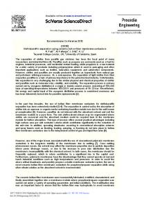
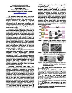
thermocatalytic gas sensors enables a superposition of advantages of both technologies. Ceramic MEMS with 12 Pm Al2O3 or ZrO2/Y2O3 membrane (Fig.1) described in [1] can operate at 600ºC, withstands technological annealing up to 1000ºC, works in harsh environment, and is characterized by perfect adhesion of platinum and other functional layers. However, the deposition of platinum heaters by magnetron sputtering leads to very high consumption of platinum and, therefore, to an increase in production cost of microhotplates. On the other hand, the application of photolithography for the patterning of microheaters requires the application of clean room equipment and increases again the production cost of MEMS devices. Screen printing usage is limited by fragility of ceramic membrane and printing resolution of ~150 Pm. As a result, such sensor consumes >150 mW, much more than silicon MEMS [2]. The application of ink and aerosol jet printing for ceramic MEMS chips of semiconductor and thermocatolytic gas sensors, fast temperature and gas flow sensors, etc. permits the fabrication of devices free of most disadvantages of silicon technology and of the techniques related with platinum sputtering and photolitography. This approach gives wireless applicable strain-free cantilever devices (Fig. 2) fabricated by laser cutting of alumina membrane, precious metals are used only for the deposition of sensor elements, printing speed is sufficient for medium scale (~1 million per year) production, and the adhesion of platinum nano-particles of the ink are characterized by perfect adhesion to alumina substrate after annealing at moderate temperature (