number of turns with optimal spacing between arms has infinite spectral efficiency and bandwidth. Practically we need to deal with the fact that the unlimited size ...
An integrated spiral antenna system for UWB Magnus Karlsson, and Shaofang Gong University of Linköping, Department of Science and Technology - ITN, LiU Norrköping, SE-601 74 Norrköping, Sweden, Phone +46 11363491
Abstract — As wireless communication applications require more and more bandwidth, the demand for wideband antennas increases as well. For instance, the ultra wideband radio (UWB) utilizes the frequency band of 3.110.6 GHz. The spiral antenna has a higher spectral efficiency than other planar antennas like the patch antenna. Theoretically, any type of antennas can be combined into different kind of arrays, in order to improve performance beyond that from one single antenna. The electrically coupled parallelism is one solution to extend bandwidth. By combining two spiral antennas with different radius of the radiation zone, the standing wave ratio (SWR) can be kept low for a large bandwidth, resulting in an improved spiral antenna performance for UWB. Furthermore, a study of how spiral dimensions impact on Gain and SWR was conducted and presented.
I. INTRODUCTION The spiral antenna has wide bandwidth, i.e., good spectral efficiency compared to other planar antennas [1]. Spiral antennas are based on Archimedes principle for a spiral, which can have many shapes depending on design goals. Theoretically a spiral antenna with an infinite number of turns with optimal spacing between arms has infinite spectral efficiency and bandwidth. Practically we need to deal with the fact that the unlimited size is not possible, and the turns cannot be too close to each other without suffering the gain. The antenna is intended for a module design in which other components will be placed on the backside of the module. Thus a ground plane is used to shield components from the antenna radiation. Therefore the antennas should be integrated on a multilayer PCB (Printed Circuit Board). Ultra wideband radio (UWB) has been specified in the frequency range 3.1 to 10.6 GHz [2]. II. OVERVIEW OF THE ANTENNA SYSTEMS
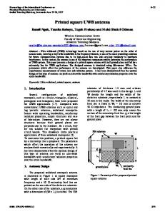
An antenna array is often used to extend antenna performance when that from a single antenna element is not sufficient. No matter which array technique used, most antennas should be connected to a 50 Ω port. Fig. 1 shows the schematics and layouts of our proposal to utilize one monofilar spiral antenna or two monofilar spiral antennas in parallel for UWB. A power divider is used in the dual antenna array solution. Antenna
(a) Single antenna solution
Pwr. div. Antenna r2
(b) Dual antenna array solution Fig. 1. Overview of the antenna system: (a) single antenna solution, and (b) array solution.
B. Substrate Table 1. Four layer PCB parameters Dielectric top Dielectric core Dielectric bottom Dielectric constant Dissipation factor Metal thickness Metal thickness Metal conductivity Surface roughness
RCC RO4350B RCC All layers All layers Top and bottom RO4350B (core) All layers All layers
Height, h=0.05 mm (1x) h=1.524 mm h=0.05 mm 3.48±0.05 0.004 25 µm 18 µm 5.8x10⁷ S/m 0.001 mm
Table 1. shows material parameters used for simulations, and Fig. 2 illustrates the cross section of the PCB. Rogers RO43xx series are used for high frequency PCBs suitable for radio frequency (RF) modules [3]. Gnd
Antenna layer
Via
Top Core Bottom
Component layer Fig. 2.
Cross section of the four layer PCB
C. Principle of the Monofilar Spiral
A. Antenna Solutions
Input
r1
Antenna Input
Radius, r
As shown in Fig. 3, the circumference of the radiation zone determines the radiation frequency. The circumference should be > 2λ [4]. If the current flowing backwards is smaller than that flowing forward, there is a net current flow through the spiral and radiation occurs. Feeding to the spiral can be done either from the centre or from the outside. In the designs shown in this paper the feeding is done by a via to the centre of the spiral (see Fig. 2). The input impedance depends on the line width together with the distance to the ground plane, because the characteristic impedance of the spiral arm is dependant of the line width as in the case of a microstrip line. The real part of the input impedance can be controlled by the line width, while the imaginary part is
Antenna
Turn distance, ∆s
1x 1x (loss-less)
Open end
Radiating zone
2x 2x-air
10 Gain (dBi)
more difficult to control. If implemented in a narrow band system the spiral antenna can be matched with a classical RF matching technique for optimal performance in that frequency region. However if a wideband operation is required the issue must be solved with other techniques.
5 0 -5 -10 3
5
7 Frequency (GHz)
Radius, r
11
(c) Gain vs. different substrates
Feed point
Fig. 3.
9
Fig. 4. Gain simulations: (a) gain vs. turn distance, (b) gain vs. the number of turns, and (c) gain vs. different substrates.
Layout of a monofilar spiral antenna
B. Monofilar Spiral Antenna of 50 Ω III. SIMULATION RESULTS A. Gain and SWR Design Considerations Fig. 4 shows gain simulations for various monofilar spiral antennas. Simulations marked with 1x are done with substrate definitions exactly as displayed in table 1 and Fig. 2. The simulation marked with 2x has the same material but with a double core layer height. Thus, the height from the antenna plane to the ground plane is 1.5 and 3.0 mm, respectively. The substrate marked with 2xair is the 1x substrate with a 1.5 mm air distance added between the ground plane and the PCB. Fig. 4a shows a series of simulations about how the distance between turns affects the antenna gain. It is seen that if the turn distance decreases the gain of the spiral antenna suffers. Fig. 4b shows that a larger number of turns improves the antenna gain, but the density of turns should not increase. Fig. 4c shows how the dielectric loss and the substrate thickness impact on the gain. Turn. dist. 1.5 mm Turn. dist 4.5 mm
Turn. dist 3 mm Turn. dist 6 mm
Fig. 5 shows the layout and voltage standing wave ratio (VSWR) simulation of a monofilar spiral antenna. To optimize performance, the real part of the characteristic impedance was calculated to be 50 Ω, i.e., the line width was calculated to be 3.43 mm with a substrate thickness of 1.5 mm. This would be optimal for all frequencies if the input impedance was kept stable for all frequencies. Three radiuses with three different turn distances for each size of the antenna were designed and simulated. It is shown in all three of the simulations in Fig. 5b-d that a more dense turn distance (∆s) provides a higher spectral efficiency. As mentioned in the introduction, in theory the infinite number of turns gives the infinite spectral efficiency. However, owing to the chosen line width and the need of spacing between turns and limited number of turns, the bandwidth is limited in our case as seen in Fig. 5b-d. Fig. 5e-h shows radiation patterns at 6.5 GHz, one cut from each antenna size and one with air core substrate is shown. The air core antenna shown in Fig. 5h has higher efficiency performance compared to Fig. 5d-g, i.e., gain relative to directivity.
Gain (dBi)
4 -1
∆s
-6
r
-11 -16 3
5
7 Frequency (GHz)
9
11
(a) Layout
(a) Gain vs. the turn distance, 1.5 mm substrate N=15
∆s=4.5 mm
4
N=5 VSWR
Gain (dBi)
4
N=10
5
-1
∆s=6.5 mm 2
∆s=5.5 mm
3 2
-6
1
-11
2
-16 3
5
7 Frequency (GHz)
(b) Gain vs. the number of turns
9
11
3
4
5
6
7
8
Frequency (GHz)
(b) Simulation, r=3 cm
9
10
11
3
∆s=5.5 mm
∆s=4.5 mm
VSWR
4
Gain and directivity (dBi)
∆s=6.5 mm
5
2 1 2
3
4
5
6
7
8
9
10
11
Frequency (GHz)
∆s=5.5 mm
∆s=6.5 mm
2
3
4
5
6
7
8
9
10
11
Frequency (GHz)
Gain and directivity (dBi)
1
∆s=4.5 mm
VSWR
2
-10 Gain
-20 -30 -40
-50 -100 -75
Gain and directivity (dBi)
Directivity
-40 -50 -100 -75 -50 -25
0
25
50
75
100
Theta (degree)
(e) Simulation at 6.5 GHz Gain and directivity (dBi)
75
100
50
75
100
-30 -40 -50 -50
-25
0
25
Fig. 5. Monofilar spiral antenna of 50 Ω input impedance: (a) Layout, (b) VSWR simulation, r=3 cm, (c) VSWR simulation, r=5 cm, (d) VSWR simulation, r=7.5 cm, (e) radiation simulation, r=3 cm, ∆s=4.5 mm, (f) radiation simulation, r=5 cm, ∆s=4.5 mm, (g) radiation simulation, r=7.5 cm, ∆s=4.5 mm, and (h) radiation simulation with an additional 1.5 mm air core, r=7.5 cm.
Gain
Directivity
0 Gain
-20 -30 -40 -50 -100 -75
50
Theta (degree)
-30
-10
25
(h) Simulation at 6.5 GHz with an additional 1.5 mm air core, r=7.5 cm
-20
10
0
-20
-100 -75
0 -10
-25
10 Directivity 0 Gain -10
(d) Simulation, r=7.5 cm 10
-50
(g) Simulation at 6.5 GHz
5
3
Directivity
0
Theta (degree)
(c) Simulation, r=5 cm
4
10
-50
-25
0
25
Theta (degree)
(f) Simulation at 6.5 GHz
50
75
100
C. Pair of Monofilar Spiral Antenna of 100 Ω Using a similar approach as in Section III-B, two antennas optimized for the 100 Ω input were designed. To use the antenna in a 50 Ω system either a matching network is utilized or an array configuration shown in Fig. 1b is used. The radius of the antennas is 73 and 84 mm, respectively. Fig. 6a shows the layout, and Fig. 6b shows the VSWR simulation. Gain figures are seen in Fig. 4c, the line marked with 2x. The real part of the combined input impedance is designed close to 50 Ω in a wide frequency band. The VSWR curve of the array is under or between the VSWR curves of the two separate antennas of 100 Ω. As seen in Fig. 6c the arrays have a bandwidth between 1.79-11 GHz and 1.8-11 GHz at VSWR