Mar 15, 2016 - applications such as big data, the Internet of Things (IoT), and wearable devices, .... multilevel switching behavior, 3V switching voltage, and.
Green curves display several successive jumps and red curves show progressive RESET process. .... be detected by conventional voltage sweep operation.
Lee et al. [22] reported on the bipolar resistive switching characteristics of a. TiN/TiOx/HfOx/TiN ..... 30 Kund M, Beitel G, Pinnow C U, et al. Conductive bridging ...
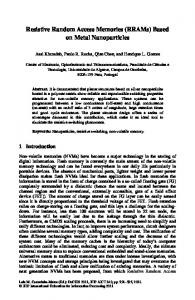
Abstract. With recent progress in material science, resistive random access memory (RRAM) devices have attracted interest for nonvolatile, low-power, ...
May 18, 2015 - field originated from nanobatteries in redox-based resistive switches29. And S. Gao, et al. demonstrated that the HRS of Cu/P3HT:PCBM/ITO ...
Feb 19, 2013 - Run-Chen Fang, Qing-Qing Sun*, Peng Zhou*, Wen Yang, ..... Sheu SS, Cheng KH, Chang MF, Chiang PC, Lin WP, Lee HY, Chen PS, Chen.
Mar 26, 2008 - arXiv:0708.1879v2 [quant-ph] 26 Mar 2008. Quantum random access memory. Vittorio Giovannetti1, Seth Lloyd2, Lorenzo Maccone3.
available [7-9]. Thin films hosting a well-defined distribution of nanoparticles are ... power, low cost, and high density memory devices is necessary for the digital.
Nongseo-dong, Giheung-gu, Yongin-si, Gyeonggi-do, 445-701, Republic of Korea ..... cell was optimized, IRESET slightly decreased compared to the previous ...
Oct 7, 2009 - Dae Keun Yun1, Ki-Don Kim1,3, Sungho Kim2, Ji-Hye Lee1,. Hyeong-Ho ..... [23] Park C W, Jeon S H, Chae S C, Han S W, Park B H, Seo S A.
Mar 17, 2014 - memory system, with two 2 GB ranks, each consisting of eight 256 MBx8, 4-bank devices [36]. Moreover, each of the 4 banks in a 256 MB ...
Jun 2, 2010 - developed based on magnetic memory elements: a magnetic latch, ..... Figure 20: Comparison of air-core and ferrite inductors vs frequency .
May 16, 2016 - ~103, low switching voltage, good cycling endurance, and long retention time ... electric field induced charge transfer effect [8,15], charge trapping/ ... tions in organic thin film transistors, solar cells, and sensors [35â40]. ...
Received February 3, 2013, accepted April 14, 2013, published May 10, 2013. Digital Object Identifier 10.1109/ACCESS. ... Read time is much less than the 6-T SRAM cell. However, write time is a .... Along with HP, Samsung and many other ...
trols the grounding of at least tWo [storage] resistive memory elements[, such as ...... Graphics Port (AGP), used to co
Disadvantages: Volatile memory, refreshing required, slow speed. Harshit
Vaishnav ... Other options like Nano RAM, Racetrack Memory etc. Harshit
Vaishnav.
Jan 17, 2010 - ... Korea, 3 Analytical Research Laboratory, Samsung Advanced Institute of Technology, PO Box 111, ... features clearly distinguishable from pristine TiO2. ... S3. An extensive examination of the SET samples revealed only six.
chalcogenide nonvolatile memory nano-cell-element based on Sb2Te3 material, Microelectron. Eng., 82(2), 168â174. 57. Gu, Y., Zhang, T., Song, Z., Liu, B., and ...
Nov 22, 2011 - storage capacity of up to 88 Gb inchâ 2, ultralow power dissipation as low as ..... (left) and 0.0364 (right), in the 64Ã64Ã35 nm3 ni-free layer. .... As shown, the optimized lateral size cannot be too big or too small, otherwise t
Jul 30, 2015 - issue of Flash temporarily [3], the market demands next- generation ..... [6] Pan F, Gao S, Chen C, Song C, Zeng F. Recent progress in resistive.
Jan 25, 2016 - -dioxythiophene):poly(styrenesulfonate) (PEDOT:PSS) where poly ... for conjugated polymer poly (3,4-ethylene-dioxythiophene) PEDOT and ...
Dec 29, 2011 - G. Bersuker,1,a) D. C. Gilmer,1 D. Veksler,1 P. Kirsch,1 L. Vandelli,2 A. Padovani,2 L. Larcher,2. K. McKenna ... breakdown, which exhibits much shorter characteristic times than the ... the energies of the injected electrons and elect
an on/off resistance ratio of 103, low set/reset voltage, and excellent data retention. .... current ratio had a stable value of â¼ 103, as shown in Fig. 1. This result is ...
Y. F. Chang 1, L. Ji 1, Y. C. Chen 3, F. Zhou 1, T. M. Tsai 4, K. C. Chang 4, M. C. Chen 4, T. C. Chang 4, B. Fowler 2, E. T. Yu 1, and J. C. Lee 1. 1 MRC, ECE, The ...
Nov 3, 2016 - Lifeng Liu, Xiaoyan Liu, Junjie Li, Changzhi Gu, Jinfeng Kang,* and Richeng Yu*. Dr. C. Li, Dr. Y. Yao, X. Guan, Dr. X. Shen,. Dr. Y. Wang, Prof.
www.advmat.de
www.advancedsciencenews.com
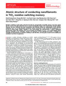
Chao Li, Bin Gao, Yuan Yao, Xiangxiang Guan, Xi Shen, Yanguo Wang, Peng Huang, Lifeng Liu, Xiaoyan Liu, Junjie Li, Changzhi Gu, Jinfeng Kang,* and Richeng Yu* Electrically induced resistive-switching (RS) phenomena are widely observed in a huge variety of dielectrics each with a metal–insulator–metal structure.[1–4] Diverse RS-based devices such as resistive random access memory (RRAM) have been demonstrated to have promising potential applications in integrated circuits and internet of things industries due to the emerging nonvolatile memory, bioinspired neuromorphic devices, hardware security solution, etc.[4–8] Understanding the microscopic mechanism of RS behavior is crucial for designing and optimizing the relevant electronic devices, propelling the theoretical research progress of the nanoscale condensed matter. So far, great efforts have been made to clarify the switching mechanisms.[9–18] Numerous methods such as electrical measurements, high-resolution X-ray photoelectron spectroscopy (XPS), Raman mapping, conductive atomic force microscopy (C-AFM), scanning electron microscopy (SEM), ex situ transmission electron microscopy (TEM), and in situ TEM were used to identify the origins of switching behaviors.[14–28] With those powerful techniques, the morphology, evolution dynamics, and chemical compositions of conductive filaments (CFs) in metal interstitial type RS devices, which are usually called conductive bridge random access memory (CBRAM) or electrochemical memory, have been extensively investigated.[16,29] However, unlike the fruitful findings in the metal bridge devices, there is still a lack of details about the evolution of the CF in oxygen-vacancy-type RS prototypes due to the difficulty in directly observing the oxygen-vacancy defects, which are
Dr. C. Li, Dr. Y. Yao, X. Guan, Dr. X. Shen, Dr. Y. Wang, Prof. J. Li, Prof. C. Gu, Prof. R. Yu Beijing National Laboratory of Condensed Matter Physics Institute of Physics Chinese Academy of Sciences Beijing 100190, P. R. China E-mail: [email protected] Dr. B. Gao, Dr. P. Huang, Prof. L. Liu, Prof. X. Liu, Prof. J. Kang Institute of Microelectronics Peking University Beijing 100871, P. R. China E-mail: [email protected] X. Guan, Prof. R. Yu School of Physical Sciences University of Chinese Academy of Sciences Beijing 100049, P. R. China
DOI: 10.1002/adma.201602976
Adv. Mater. 2017, 1602976
usually called oxide-based RRAM (OxRRAM) or valence change memory (VCM).[19,22–25,29] Up to now, several fundamental issues of the elusive switching mechanism in these transitionmetal oxides have been still under debate, for example, how the CF is built up while oxygen vacancies are forming, where the CF starts to grow in the forming process, where the CF ruptures in the RESET process, etc.[9–19] A few of researches on VCM by in situ TEM focused on the conductive crystallites of Magnéli phase in TiO2-based RRAM,[19] TaO2−x dendrites in Ta2O5−x layer[22,23] and zinc precipitants in ZnO film,[25] which are generated when oxygen is extracted by the electric field strength and can be characterized by the traditional contrast recognition or diffraction analysis through combining the characteristic electron energy loss spectrum (EELS) and energyfiltered image (EFI) to identify the oxygen concentrations of the reduced products in the insulation layers, thereby testifying the oxygen concentration variation under the electric bias. However, crystalline oxygen-deficient phases seldom occur in most of transition-metal oxides, such as the HfO2-based architecture, which still exhibits RS behaviors with the believable assistance of oxygen vacancies.[30–32] New methods are eager to be developed to illustrate the oxygen concentration variation in real time. In addition, there is no concrete evidence to prove the electrons flowing in the oxygen-vacancy channel due to the difficulty in directly observing the CF configuration despite of the hypothesis equivalence of the CFs and the oxygen-vacancy channels. Furthermore, where the switch happens is still an open question because the formed oxygen-deficient phase cannot supply the substantial information about the rupture process of the CF, even though some models have been suggested.[4,10,13,14,18,33–35] Therefore, the direct characterizations of the oxygen vacancies and CF behaviors, including the generation, the evolution and the morphology, are urgently needed to clarify the discrepancy in the CF composition, the formation and disruption dynamics in OxRRAM. Recently, in situ electron holography has become a powerful tool to image the electrostatic potential distribution in a semiconductor device in TEM.[36] The charges accumulated in the biased sample can change the phase of the transmitted electron wave, and such a phase disturbance can be retrieved from the electron interference patterns.[36,37] So the formations and ruptures of the CFs in the VCM may be revealed in real space by electron holography. Moreover, in situ low-energy-filtered images can describe the oxygen concentration changes in the hafnia films.[38] Here, the repeatable RS processes in HfO2based RRAM are investigated by using TEM with electron
Direct Observations of Nanofilament Evolution in Switching Processes in HfO2-Based Resistive Random Access Memory by In Situ TEM Studies
www.advancedsciencenews.com
COMMUNICATION
www.advmat.de
Figure 1. a) Schematic diagram of in situ experiment and b) a series of I–V measurements showing reversible bipolar resistive switching.
holography and in situ low-energy-filtered imaging, and in situ electrical characteristic measurements to reveal the relationship between the oxygen-vacancy distribution and the CF formation and rupture, and the I–V behaviors as well, through combining with the morphology information. The acquired results demonstrate that the oxygen vacancies are generated in the SET process. The images also confirm that the density of oxygen vacancies is reduced due to the recombination with oxygen ions, and that the CFs are ruptured near the cathode interface in the RESET process as described in refs. [12] and [33]. Figure 1a shows the schematic diagram of the in situ measurement. The HfO2-based RRAM cross-section samples fabricated by focused ion beam (FIB) technology are operated inside a TEM to enable the real-time observation of the voltageinduced structural and chemical changes, including the conduction channels. Several samples are sliced at the same time from a wafer for in situ I–V measurement, holography study and EELS imaging, respectively. The Au tip approaches the top electrode (TE) while the bottom electrode (BE) is grounded. The initial switching behavior of the RRAM device inside the TEM is measured by in situ measuring the I–V characteristics at various voltages as shown in Figure 1b. The fresh devices are of the high resistance state (HRS). Before the direct current
sweeping, a forming process up to 7 V takes place on the asprepared device to turn the device into a low resistance state (LRS) device. The RESET voltage is about −6.5 V at first. Then, when the voltage bias varies as 0 V→4 V→0 V→−3 V→0 V, the repeatable bipolar switching behaviors from HRS to LRS (SET) and from LRS to HRS (RESET) are observed. The compliance current is limited below 0.1 mA in the forming process but increased to 1 mA for SET and RESET operation. When the compliance current is restricted below 1 mA, the current of HRS is undetectable due to the detection limit as indicated in Figure 1b. The repetitive test above for a thicker sample is shown in Figure S1 (Supporting Information). Figure 2 displays the amorphous HfOx film within the clear multilayer stacks. The AlOy layer is inserted at the interface between the HfOx film and Pt to enhance the repeatability and stability of RS behaviors[39] and make it easy to distinguish the HfOx film from the retrieved potential map. Contrary to the titanium or tantalum oxide RS device where the oxygen-deficient compound has a quite different crystal structure which can be distinguished readily by the contrast or diffraction change,[19,22,23] it is difficult to separate the nonstoichiometric HfOx phase straightforwardly from HfO2 in the ordinary TEM/scanning transmission electron microscopy
Figure 2. a) High-angle annular dark-field (HAADF) image of an RRAM cross-section sample, b) high-resolution TEM (HRTEM) images, and c) the retried phase maps (without bias) of the dielectric layers in the red rectangular region marked in panel (a).
and most of positive charges are aggregated near the top interface between the HfOx film and AlOy layer as shown in Figure 3b,c. When bias is above 3 V, the potential of the AlOy layer changes to nearly zero and then to a negative value. At the same time, a demonstrable negative potential emerges in the lower half of the hafnia layer and diffuses vertically toward the top interface of the HfOx film. The retrieved potential maps still illustrate the relic of the charges left in the HfOx film under the preset bias, although they are acquired after the bias has been withdrawn. The origin of the positive charges could be related to the oxygen vacancies, which will be clarified later, while the negative potential is contributed from the transport electrons residual in the migration path, which can track the formation of CF in the oxide film. Several negative potential branches even reach the TE (anode) at 7 V (Figure 3g), at which the device turns into the LRS and thus the forming process is completed. A series of snapshots in Figure 3 exhibits unambiguously the dynamical formations of CFs when the device transforms from the HRS into the LRS. To monitor the behaviors of the CFs when switched from the LRS to the HRS, the hologram images of the HfO2-based
Figure 3. Bias-induced phases featuring Δϕbias (x,y) under different positive biases in the forming process, where the intrinsic inner potential is removed by using the phase image of the pristine sample without any bias. The images are retrieved from the holograms taken at zero voltage after the corresponding bias setting. Only the HfOx film is highlighted here. Dark red is for higher potential while dark blue is for the lower potential. The dashed curve outlines the boundary between the positive and negative phases. The scale bar means the phase values.
(STEM) image. Because the electron traveling along the CFs can induce the potential changes in the functional hafnia layer, electron holography is employed to detect the potential variation after applying bias and to deduce the evolution of the CF in the RS process. After a voltage setting, the bias is released and the electron holography images (holograms) of the HfO2-based RRAM device are recorded; then the applied bias jumps to the next value and released again to record a new corresponding hologram image, and so on. After stripping off the intrinsic inner potential and the dynamic diffraction effect from the pristine state of the sample, the bias-induced phase featuring Δϕbias (x,y) of the HfOx film reflects the projected electric potential evolutions in the HfOx film under different biases (during forming) and RESET conditions since the difference between the phase and the potential is just an interaction constant.[36] So Δϕbias (x,y) refers to both the phase map and the potential map indiscriminately for convenience herein below. If the positive bias is applied to the TiN TE (anode) of the fresh device, the positive potential is induced initially, which implies that the positive charges are generated in the whole oxide layer (Figure 3a). Increasing bias may enhance the positive potential,
www.advancedsciencenews.com
COMMUNICATION
www.advmat.de
Figure 4. Bias-induced phases featuring Δϕbias (x,y) under different negative biases in the RESET process, where the intrinsic inner potential is removed by using the phase image of the pristine sample without any bias. The images are retrieved from the holograms taken at zero voltage after the corresponding bias setting. Dark red is for higher potential while dark blue is for the lower potential. The dashed curve outlines the boundary between the positive and negative phases.
RRAM device are acquired under negative bias in the RESET process for the same sample shown in Figure 3. The retrieved Δϕbias (x,y) shown in Figure 4 indicates clearly that the negative potential synapses retract from the TE (cathode) eventually with the negative bias force increasing. With the RESET voltage increasing, the density of oxygen vacancies in CFs decreases near the electrode. At −3 V, one of the two filaments (on the right) starts to rupture. At −5 V, the other filament also starts to rupture in its neck. Two negative tentacles are left near the TE (cathode) and the CFs are ruptured at about −6.5 V, which is consistent with the monitored I–V curve. Part of AlOy layer recovers to nearly neutral state but a negative channel remains there. It should be emphasized that electron holography can only detect the net project potential determined by the dominant charges but cannot recognize a few of positive charges buried under the injected electrons at the lower half of the HfOx film even if they actually exist, and it cannot recognize the protruding electrons embedded in the positive charges matrix in the upper half part of the film either. Thus the details of the positive charges can be investigated in depth to unveil the mechanism of the forming behavior. 1602976 (4 of 8)
wileyonlinelibrary.com
EELS in TEM is an appropriate method to characterize the chemical states of the elements in the RRAM sample. Unlike the conventional fingerprint energy characteristics, plasmon resonance absorption feature is involved here to map the oxygen concentration variation during the forming operation because the peak in the low-energy-loss spectrum of the HfO2 is sensitive to the oxygen concentration of the hafnia film.[40] The peak at 26 eV should increase, opposite to the peak at 16.4 eV, as the oxygen content decreases, exhibiting the lowloss spectra of low and high oxygen content HfO2 samples. So the relative height variation between the peaks at 16.4 and 26 eV can be employed to estimate the oxygen consumption in the storage layer: the increase of the peak at 26 eV indicates the dissipation of the oxygen, or the generation of oxygen vacancies.[38,40] As indicated experimentally, the energy loss centers are situated at 24 eV for the filtered image and 4 eV for the energy window, respectively, therefore the 26 eV peak and the 16.4 eV peak are efficiently separated from each other. Another advantage of the plasmon mapping is that the intensity of the signal is a few orders of magnitude higher than the characteristic high energy peaks, which improves the S/N ratio and
COMMUNICATION Figure 5. Low-loss energy-filtered images of the RRAM under different positive biases, demonstrating that the concentration of the oxygen varies with increasing positive bias (red denotes the higher oxygen concentration). The dashed curve outlines the OXYGEN-RICH domain, which shrinks under positive bias.
shortens the exposure time, thus avoiding the annoying image drift. Figure 5 describes the variations of oxygen vacancies or the oxygen concentration fluctuations under different biases in the forming process. Despite the uneven distribution of the oxygen vacancies in the fresh sample (Figure 5a), an overall change is the proliferation of the oxygen vacancies in the whole hafnia film as the positive bias rises, if the initial status is compared with the resulting status. Unlike the model established for the TiO2-based devices where the oxygen vacancies are thought to protrude from the TE (anode) to the BE (cathode),[19] the in situ images here demonstrate that the oxygen vanish inhomogeneously in the oxide layer while they escape much faster near the anode (TE). The vacancies are preferably created near the top interface but they are also distributed in other parts, especially aggregate at some locations of bottom interface. The vacancy diffusion front is irregular and the morphology of the protrusions is not stable until the bridges are built up when the bias is above 5 V. The shapes of vacancy channels may be changed even at the LRS. It should be stressed that the energy-filtered images are acquired when the bias is kept unchanged and the sample slice is not the same one for the in situ forming and RESET test because it is hard to collect the EELS signal and hologram simultaneously in TEM. The observed oxygen vacancies with positive charges near the top interface should contribute to the positive potential stripe in the phase maps (Figure 3 and 4), while the vacancies at the bottom of the oxide layer are neutralized by the poured electrons even though the oxygen insufficiency state can be still figured out by EELS. From the electron holography images and low-loss energyfiltered images, the sketch of the CFs formation can be outlined. The external bias can dissociate the HfO bands and Adv. Mater. 2017, 1602976
induce the generation of additional oxygen vacancies in the bulk of hafnia layer[33,38] as shown in Figure 5. Initially, the generated oxygen vacancies are positive charges which act as the positive potential in Figure 3a–c. The potential maps also indicate that bias may induce positive oxygen vacancies in the AlOy layer, which is reasonable though the EELS mapping can give no such conclusion due to the lack of experimental evidence for the relationship between the intensity of low-loss energy peak of AlOy and the oxygen concentration. This fast vacancy generation process is quite different from those of the single crystal STO-based RRAM and CBRAM in which the point defects diffuse from one of the electrode interfaces to the bulk of switching layer.[15,16] As bias increases, the electrons are injected into the oxide layer, and the oxygen vacancies and other defects can trap some injected electrons, so some parts of the HfOx and AlOy films turn to be of negative potential. These trapped negative electrons can be seen as the trace marker of the CFs. The holography and EELS mapping images of the forming process (Figure 3 and 5) show that the filaments built by the oxygen vacancies with high density gradually emerge in the HfOx film. Meanwhile the electrons will fill the AlOy film and the lower surface of the HfOx film along the formed filaments under the positive bias but accumulate there and move upward slowly due to the insulating property of the oxide, which reasonably occurs similarly in the way the charge trap memories do.[36] If the bias is above 4 V, the oxygen-vacancy bridges can be realized so that the impeded electrons find the quick ways toward the TE (anode). When the stable vacancy bridges form under a bias of above 6 V, the CFs reach the TE (anode) from different positions. Although the electrons may flow through the oxygen-vacancy channel, the shape of the electron current is determined by the local resistance which may not be uniform
along the vacancy path. Electrons will find their fastest ways to the TE (anode) automatically so the percolation path, not the size of the oxygen-vacancy bridge controls the shape of the CF. It also shows that the growth of percolation path where the electrons pass through and oxygen vacancies path follow the same trend, and thus the percolation path is formed owning to the formation of oxygen vacancies filament. In the RESET process, the CFs rupture in the fragile bottleneck near the top interface because negative bias could release the oxygen ions stored in the TE (cathode)[12,33,41] to annihilate the oxygen vacancies easily there as shown in Figure 4 where the positive potential range beneath the TE (cathode) becomes fragmented under negative bias. Moreover, plenty of residual oxygen vacancies near the TE (cathode) ensure that the CFs will be recovered quickly under proper positive bias. This recombination process between oxygen vacancies and movable oxygen ions is different from the unipolar switch behavior where the fuse mechanism may dominate the RS action.[19,42] The rupture site located near the TE (cathode) is also different from those from some analytical models in which the CF ruptures happen in the middle of or near the BE (anode). At the same time, the potential in AlOy layer recovers partially but there are still lots of negative electrons which maintain the conductivity of the AlOy layer. The RS processes are summarized in Figure 6 according to the direct observations by in situ TEM and Monte Carlo simulations based on the physical model[12,33] (the simulation method can be found in the Supporting Information). In the forming process, the oxygen vacancies are generated gradually as the positive bias turns high enough to dissociate the Hf-O bands. At the same time, the injected electrons appear and accumulate at the bottom interface of the HfOx film under the positive bias.
When the oxygen vacancies form the channels connecting the two electrodes, the CFs are built up. The electrons pass through the oxygen-vacancy bridge and the device turns from the HRS to the LRS. Then the forming process is completed. In the RESET process, the oxygen vacancies near the top interface should be depleted at the negative bias and the CFs are broken first near the TE (anode) thus the device turns into the HRS. However, the shape of the CF is independent of the shape of the oxygen-vacancy channel. Lots of oxygen vacancies remain near the top interface of the HfOx film, so the bias switching from the HRS to the LRS in SET is smaller than that in the forming process. The resistive switching processes in a HfO2-based RRAM are investigated by electron holography and in situ energyfiltered imaging with applied biases. Experimental data demonstrate that the CFs are formed due to the fact that the oxygen vacancies are generated and ruptured at the top interface of the HfOx film. In the forming process, positive bias produces a lot of oxygen vacancies at the top interface but some vacancies also gather at the bottom interface, accompanied with injected electrons. As the positive bias increases, the oxygen vacancies multiply and diffuse in the HfOx film. Finally, they form the continuous channels connecting two electrodes where the electrons can drift more easily and reach the anode. The oxygen-vacancy channels may be broad but the bottlenecks of the CFs are near the TE. In the RESET process, the electron holography data show that the CFs may shrink from the top interface and rupture near the TE side. These pictures reveal the details of the bipolar switching behaviors and clarify the physical mechanism behind the conventional I–V measurement. Those findings can not only contribute to
Figure 6. Schematic diagrams of the RS processes in HfO2-based RRAM. From the top to the bottom sequentially are the forming process, RESET process, and SET process. First column: dynamic process; second column: simulated CF; third column: experimental potential maps.
Experimental Section Devices Fabrication: The HfO2-based RRAM sample was prepared as follows. First, a 20 nm Ti adhesion layer and a 100 nm Pt bottom electrode layer were deposited on a 4 in. N+Si substrate (ρ ≈ 0.002–0.006 Ω cm) by physical vapor deposition. Then 5 nm Al2O3 and 9 nm HfO2 layers were deposited by atomic layer deposition at 300 °C, using H2O and trimethylaluminum/tetrakis [ethylmethylamino] hafnium as precursors. After that, a 100 nm TiN top electrode layer was deposited by reactive sputtering at room temperature in the Ar and N2 mixture with Ar:N2 = 18:2. Finally, photolithography and dry etching were performed to isolate the device cells on the wafer. TEM Sample Preparation: The cross-section RRAM samples were mechanically milled into small pieces of about 10 µm thick and then cut them by FIB technique with ±2° refinement to guarantee the uniform thickness. Additional 20 s Ar ion milling was carried out to remove the surface amorphous layers and the possible dead layers. The thickness of the final TEM specimen was about 50 nm measured by EELS technique, which is shown in Figure S2 (Supporting Information). The sample was loaded on a Nanofactory in situ holder, in which Au tip could be used to apply the voltage to the TiN gate of the sample and monitor the current at the same time. TEM Observations: Conventional HRTEM, HAADF, the low-loss energy-filtered images, and electron hologram were obtained by using a field-emission gun TEM (FEI Tecnai F20). Electron holograms were recorded by a charge-coupled device camera. Standard vacuum reference hologram was acquired first to correct the phase distortion from the optical system. The electron holograms were recorded with the reference wave penetrating the TiN gate because the limited view field of hologram at high magnification cannot cover the vacuum region over the HfOx and AlOy layers, which is deep below the TiN gate. Using the vacuum as reference (Figure S3, Supporting Information), the spatial electron holography is estimated at about resolution of 0.43 nm (qc = 6.94 nm−1, qc /3 is used to reconstruct the phase image). The holography reconstruction was realized with the plug-in HoloWork in Digital Micrograph of Gatan, and the unwrapping processing was achieved with a published code.[43] The error of the phase retrieve is less than 0.2 rad, measured from the TiN electrode which was assumed to be an equipotential body.
Supporting Information Supporting Information is available from the Wiley Online Library or from the author.
Acknowledgements C.L., B.G., and Y.Y. contributed equally to this work. R.C.Y. and J.F.K. designed the research project and supervised the experiments and calculations. B.G., P.H., L.F.L., X.Y.L., and J.F.K. fabricated HfO2-based RRAM devices and performed the relevant theoretical calculations. C.L. and X.X.G. fabricated TEM samples using FIB technique with the help of J.J.L. and C.Z.G. C.L. carried out TEM experiments and analyzed data with the help of Y.Y., X.S., Y.G.W., and R.C.Y. C.L., Y.Y., and R.C.Y. wrote the paper, in which the results and text are discussed by all the authors. This work was supported by the National key research program of China
Adv. Mater. 2017, 1602976
(Grant Nos. 2016YFA0300701 and 2013CB932904) and the National Natural Science Foundation of China (Grant Nos. 11374343, 61421005, 11574376, and 61334007). Received: June 6, 2016 Revised: November 3, 2016 Published online:
[1] T. W. Hickmott, J. Appl. Phys. 1962, 33, 2669. [2] R. Waser, M. Aono, Nat. Mater. 2007, 6, 833. [3] A. Sawa, Mater. Today 2008, 11, 28. [4] H. S. P. Wong, H. Y. Lee, S. M. Yu, Y. S. Chen, Y. Wu, P. S. Chen, B. Lee, F. T. Chen, M. J. Tasi, Proc. IEEE 2012, 100, 1951. [5] J. J. Yang, D. B. Strukov, D. R. Stewart, Nat. Nanotechnol. 2013, 8, 13. [6] M. J. Lee, C. B. Lee, D. Lee, S. R. Lee, M. Chang, J. H. Hur, Y. B. Kim, C. J. Kim, D. H. Seo, S. Seo, U. I. Chung, I. K. Yoo, K. Kim, Nat. Mater. 2011, 10, 625. [7] M. Prezioso, F. M. Bayat, B. D. Hoskins, G. C. Adam, K. K. Likharev, D. B. Strukov, Nature 2015, 521, 61. [8] A. Chen, Tech. Dig. - Int. Electron Devices Meet. 2015, 265. [9] K. Szot, W. Speier, G. Bihlmayer, R. Waser, Nat. Mater. 2006, 5, 312. [10] S. Larentis, F. Nardi, S. Balatti, D. C. Gilmer, IEEE Trans. Electron Devices 2012, 59, 2468. [11] S. H. Chang, J. S. Lee, S. C. Chae, S. B. Lee, C. Liu, B. Kahng, D. W. Kim, T. W. Noh, Phys. Rev. Lett. 2009, 102, 026801. [12] B. Gao, J. F. Kang, Y. S. Chen, F. F. Zhang, B. Chen, P. Huang, L. F. Liu, X. Y. Liu, Y. Y. Wang, X. A. Tran, Z. R. Wang, H. Y. Yu, A. Chin, Tech. Dig. - Int. Electron Devices Meet. 2011, 417. [13] S. Kim, ACS Nano 2014, 8, 2369. [14] I. Valov, E. Linn, S. Tappertzhofen, S. Schmelzer, J. V. D. Hurk, F. Lentz, R. Waser, Nat. Commun. 2013, 4, 1771. [15] K. Shibuya, R. Dittmann, S. Mi, R. Waser, Adv. Mater. 2010, 22, 411. [16] Q. Liu, S. B. Long, H. B. Lv, W. Wang, J. B. Niu, Z. L. Huo, J. N. Chen, M. Liu, ACS Nano 2010, 4, 6162. [17] H. Tian, H. Y. Chen, B. Gao, S. M. Yu, J. L. Liang, Y. Yang, D. Xie, J. F. Kang, T. L. Ren, Y. G. Zhang, H. S. P. Wong, Nano Lett. 2013, 13, 651. [18] U. Celano, L. Goux, R. Degraeve, A. Fantini, O. Richard, H. Bender, M. Jurczak, W. Vandervorst, Nano Lett. 2015, 15, 7970. [19] D. H. Kwon, K. M. Kim, J. H. Jang, J. M. Jeon, M. H. Lee, G. H. Kim, X. S. Li, G. S. Park, B. Lee, S. Han, M. Kim, C. S. Hwang, Nat. Nano 2010, 5, 148. [20] Q. Liu, J. Sun, H. B. Lv, S. B. Long, K. B. Yin, N. Wan, Y. T. Li, L. T. Sun, M. Liu, Adv. Mater. 2012, 24, 1844. [21] U. Celano, L. Goux, A. Belmonte, K. Opsomer, A. Franquet, A. Schulze, C. Detavernier, O. Richard, H. Bender, M. Jurczak, W. Vandervorst, Nano Lett. 2014, 14, 2401. [22] J. Y. Chen, C. W. Huang, C. H. Chiu, Y. T. Huang, W. W. Wu, Adv. Mater. 2015, 27, 5028. [23] G. S. Park, Y. B. Kim, S. Y. Park, X. S. Li, S. Heo, M. J. Lee, M. Chang, J. H. Kwon, M. Kim, U. I. Chung, R. Dittmann, R. Waser, K. Kim, Nat. Commun. 2013, 4, 2382. [24] F. Miao, Adv. Mater. 2011, 23, 5633. [25] J. Y. Chen, C. L. Hsin, C. W. Huang, C. H. Chiu, Y. T. Huang, S. J. Lin, W. W. Wu, L. J. Chen, Nano Lett. 2013, 13, 3671. [26] Y. C. Yang, P. Gao, S. Gaba, T. Chang, X. Q. Pan, W. Lu, Nat. Commun. 2012, 3, 372. [27] J. P. Strachan, M. D. Pickett, J. J. Yang, S. Aloni, A. L. D. Kilcoyne, Adv. Mater. 2010, 22, 3573. [28] M. Sowinska, T. Bertaud, D. Walczyk, S. Thiess, M. A. Schubert, M. Lukosius, W. Drube, Ch. Walczyk, T. Schroeder, Appl. Phys. Lett. 2012, 100, 233509.
designing and fabricating the better RRAM devices but also facilitate more comprehensive understanding of the relevant phenomena induced by the electric bias in many semiconductor devices, such as the failure mechanism about the gate insulator in the transistors or the charge transport in the flash memories.
COMMUNICATION
www.advmat.de
www.advancedsciencenews.com
[29] R. Waser, R. Dittmann, G. Staikov, K. Szot, Adv. Mater. 2009, 21, 2932. [30] F. D. Stefano, M. Houssa, J. A. Kittl, M. Jurczak, V. V. Afanas’ev, A. Stesmans, Appl. Phys. Lett. 2012, 100, 142102. [31] P. Huang, X. Y. Liu, B. Chen, H. T. Li, Y. J. Wang, Y. X. Deng, K. L. Wei, L. Zeng, B. Gao, G. Du, X. Zhang, J. F. Kang, IEEE Trans. Electron Devices 2013, 60, 4090. [32] H. Y. Lee, Y. S. Chen, P. S. Chen, P. Y. Gu, Y. Y. Hsu, S. M. Wang, W. H. Liu, C. H. Tsai, S. S. Sheu, P. C. Chiang, W. P. Lin, C. H. Lin, W. S. Chen, F. T. Chen, C. H. Lien, M. J. Tsai, Tech. Dig. - Int. Electron Devices Meet. 2010, 460. [33] B. Gao, B. Sun, H. W. Zhang, L. F. Liu, X. Y. Liu, R. Q. Han, J. F. Kang, B. Yu, IEEE Electron Device Lett. 2009, 30, 1326. [34] Y. Z. Guo, J. Robertson, Appl. Phys. Lett. 2014, 105, 223516. [35] A. Padovani, L. Larcher, G. Bersuker, P. Pavan, IEEE Trans. Electron Devices 2015, 62, 1998.
1602976 (8 of 8)
wileyonlinelibrary.com
[36] Y. Yao, C. Li, Z. L. Huo, M. Liu, C. X. Zhu, C. Z. Gu, X. F. Duan, Y. G. Wang, L. Gu, R. C. Yu, Nat. Commun. 2013, 4, 2764. [37] P. A. Midgley, R. E. D. Borkowski, Nat. Mater. 2009, 8, 271. [38] C. Li, Y. Yao, X. Shen, Y. G. Wang, J. J. Li, C. Z. Gu, R. C. Yu, Q. Liu, M. Liu, Nano Res. 2015, 8, 3571. [39] Y. S. Chen, B. Chen, B. Gao, L. F. Liu, X. Y. Liu, J. F. Kang, J. Appl. Phys. 2013, 113, 164507. [40] J. H. Jang, C. S. Hwang, H. S. Jung, M. Kim, J. H. Kim, S. Y. Lee, J. Appl. Phys. 2011, 109, 023718. [41] S. M. Yu, H. Y. Chen, B. Gao, J. F. Kang, H. S. P. Wong, ACS Nano 2013, 7, 2320. [42] K. M. Kim, D. S. Jeong, C. S. Hwang, Nanotechnology 2011, 22, 254002. [43] D. C. Ghiglia, M. D. Pritt, Two-Dimensional Phase Unwrapping: Theory, Algorithms, and Software, John Wiley & Sons, Inc., New York, 1998.