arXiv:cond-mat/9905130v1 [cond-mat.mtrl-sci] 10 May 1999 ... thin film material which consists of sets of curved graphene sheets mixed with amorphous.
arXiv:cond-mat/9905130v1 [cond-mat.mtrl-sci] 10 May 1999
Carbon films with a novel sp2 network structure. I. Alexandrou1,2, H.-J. Scheibe3 , C. J. Kiely1 , A. J. Papworth2,1 , G. A. J. Amaratunga2,4 and B. Schultrich3 1
Department of Materials Science and Engineering, University of Liverpool, Liverpool L69 3BX, UK. 2 Department of Electrical Engineering and Electronics, University of Liverpool, Liverpool L69 3BX, UK. Fraunhofer Institute of Material and Beam Technology, D - 01277 Dresden, Germany. 4 Department of Engineering, Cambridge University, Cambridge CB2 1PZ, UK.
3
Abstract Laser-Arc evaporation of a graphite target has been used to deposit carbon films that exhibit high hardness (45 GPa) and elastic recovery (85%). High Resolution Electron Microscopy (HREM) and Electron Energy Loss Spectroscopy (EELS) were subsequently used to study the microstructure and bonding of the resultant layers. The structure of the films from HREM is seen to consist of a dense array of parallel curved graphene sheet segments packed in various orientations. EELS reveals that the films are comprised of mainly sp2 bonded carbon. The results suggest that a new form of carbon thin film with fullerene-like structure can be realised. In order to explain how a predominantly sp2 bonded material can exhibit such a high hardness, a simple model is proposed to correlate the excellent mechanical properties with the observed structure.
1
Introduction
The production of hard carbon based materials using cathodic arc [1] and laser ablation [2] techniques has been reported previously. High film hardness has been attributed 1
I. Alexandrou et al
2
to the presence of a high percentage of sp3 (diamond - like) bonds, whereas a high concentration of sp2 (graphitic) bonds is regarded as leading to the formation of soft films. However, the discovery of the C60 fullerene molecule [3,4] and carbon nanotubes [5] which are sp2 bonded, opens up the possibility of obtaining 3-D structures which exploit the extremely strong [6] in-planar bonds of graphite (stronger than diamond) in a new class of hard thin film materials. The reports of the formation of hard sp2 bonded materials by anisotropically pressing C60 [7, 8] and by embedding distorted fullerene - like nanoparticles in an amorphous carbon matrix [9] were early indications that such a carbon material could be synthesised. However, the structure of such high fraction sp2 bonded materials with superior mechanical properties is not known in detail. In this paper we report a novel microstructure of hard and elastic carbon films [10] prepared via a laser initiated pulsed cathodic arc method (Laser-Arc). Both High Resolution Electron Microscopy (HREM) and Electron Energy Loss Spectroscopy (EELS) show evidence for a new form of carbon thin film material which consists of sets of curved graphene sheets mixed with amorphous carbon in which sp2 carbon bonding dominates. Although a curved graphene sheet structure has previously been proposed for CNx materials [11, 12], this is the first time that HREM and EELS have been used together in order to get a more complete view of both structure and bonding in a pure carbon material.
2
Mechanical Properties
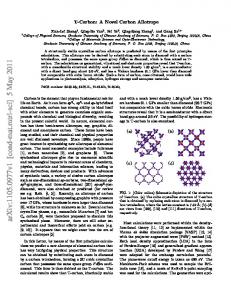
The hard and elastic films were prepared using a carbon plasma produced by the LaserArc method without any gas ambient [13]. Films deposited by this method on Si substrates typically have Youngs modulus values of E = 400 - 700 GPa as measured using laser induced acoustic waves [14]. The value depends on the specific deposition conditions (e.g. substrate temperature and arc current). For the sample under investigation a Youngs modulus of E = 480 GPa was determined. A nominal hardness of H = 45 GPa and an elastic recovery of 85% has been measured from indentation experiments. A typical microindentation curve from such a film is shown in Figure 4. The plastic hardness
I. Alexandrou et al
3
quoted was calculated on the basis of the well known Olivier and Pharr method [15, 16] from the indentation curves. There is some doubt regarding the absolute accuracy of the hardness obtained by this method. Nevertheless, the hardness is consistent with the rule of thumb H ≈ E / 10, which is well proven for amorphous carbon films. The very distinct characteristic of these films is the very small overall indentation depth and the very high elastic recovery after being subjected to a maximum load of the magnitude shown in Fig. 4. This is a clear indication of a minimal plastic deformation regime. Most other thin films (other than diamond) will show strong evidence of plastic deformation at such load levels [17]. On the other hand, a soft and elastic film, for example rubber, will show a very high degree of elastic recovery, but the maximum indentation depth would be an order of magnitude larger. Therefore, indentation characteristics such as those measured from Fig. 4 are a clear signature of thin films with superior mechanical properties.
3
Microstructural characterisation
HREM studies were carried out using a JEOL 2000EX microscope having a 0.21 nm point to point resolution, whereas a VG HB601 STEM with a 1 nm probe diameter was employed to collect the EELS spectra. The HREM and EELS analyses were performed on samples prepared by cleaving the specimen perpendicular to the interface. No preparation treatments involving ion beams or chemical etching were used. This significantly reduced the possibility of introducing microstructural artifacts. Figures 4 (a) and (b), show cross-sectional HREM micrographs taken under differing defocus conditions from the same thin area of the specimen. They reveal a structure which is very different from that usually seen in amorphous carbon films. Parallel curved fringes grouped together in sets are mixed forming patterns of swirls and concentric rings, of typically 4-6 nm in outer diameter. Selected area diffraction (SAD) showed two broad diffuse rings at around 0.113 nm and 0.210 nm, which arise from the amorphous carbon. In addition, a much sharper ring was seen centred at 0.363 nm but with an actual spread between 0.358 and 0.368 nm. These values were determined using the Si substrate mate-
I. Alexandrou et al
4
rial as calibration for the SADP. The 0.363 nm spacing is consistent with the calculated spacing between the carbon layers in bucky onion structures [18]. The shape of the fringes suggests that they represent curved graphene sheets similar to those found in carbon nanotubes and bucky onions [9, 10]. These images seem to suggest that a substantial part of the film is made up from fragments of such nanoparticles mixed in a random way forming a co-continuous matrix with the amorphous carbon component. As the specimen thickness increases beyond 25 nm, it becomes progressively more difficult to see the individual graphene sheets and the film takes on a classic “amorphous” appearance. The characteristic pattern formed by the graphene sheets is seen much more clearly in Fig. 4 (b) which is taken close to Gaussian focus, as compared to Fig. 4 (a) which was taken close to Scherzer defocus. The details of the image contrast in these HREM images are controlled by the contrast transfer function of the microscope. The frequencies of interest are 2.75 nm−1 which corresponds to the graphene plane spacing (0.363 nm) and the region around 4.76 nm−1 which correspond to the range of atomic spacings about 0.21 nm which are the periodicities associated with the diffuse diffraction ring often observed in amorphous carbon (a-C). This latter 0.21 nm spacing is close to the (100) graphite and {111} diamond spacings and can be associated with either type of short range order in a-C. Calculations of the contrast transfer function of our microscope have been performed for Scherzer and Gaussian focus conditions. In both situations the 0.363 nm (graphene) periodicity is faithfully transferred. However, in the latter case the amorphous periodicities around 0.21 nm are heavily attenuated relative to that for Scherzer defocus. Consequently, for the image at Gaussian focus, Fig. 4 (b), the graphene-like features are accentuated at the expense of the amorphous component. It is also possible to accentuate the graphene periodicities in the Scherzer defocus micrograph using image processing techniques. For example, the Fast Fourier Transform (FFT) of the area indicated in Fig. 4 (a) has been filtered to remove low periodicities and subsequently back transformed to produce the clearer image shown in Fig. 4 (c). Once again the curved graphene plane features become strongly visible at the expense of the amorphous background.
I. Alexandrou et al
5
Electron Energy Loss Spectroscopy was chosen as the most appropriate tool for studying the bonding configuration in the carbon network. Since this technique has been used extensively for carbon films in the past [19], correlation between our film and other hard carbon materials reported to-date are possible. Figure 4 shows EELS spectra acquired from different parts of the film. The 1s − σ ∗ peak at 292 eV is the signature of σ-bonding while the 1s − π ∗ peak at 285 eV indicates π bonding in our material. The ratio of the integrals under the two peaks is frequently used to estimate the amount of π bonding present [19]. Effects due to background, plural scattering and zero loss energy width have been deconvoluted from all these spectra. The result of these effects needs to be carefully considered to obtain an accurate measure of the 1s − π ∗ energy loss. We used a C60 fullerite crystal as the calibration material since it has a known 1:3 ratio of π to σ bonds and is free from the orientational effects which can arise in graphite [20]. Equating the heights of the 1s − σ ∗ peaks for all spectra, we can gain qualitative information about the fraction of π-bonding in our material by directly comparing the intensity of the 1s − π ∗ peaks. Spectrum 4(a) shows the C K-edge of a pure C60 fullerite crystal which is taken as the representation of a purely sp2 material with randomised bond orientation. Spectrum 4(b) shows the C K-edge from a highly oriented graphite sample with the basal planes parallel to the incident beam direction (i.e. the p orbitals are perpendicular to the optical axis). This spectrum is used as a reference for the maximum orientational enhancement of the 1s − π ∗ peak that could occur for the convergence and collection angles employed in this study [20]. Comparing spectra 4(a) and 4(b) we see that although both materials studied consist of sp2 bonded carbon, the orientation of the basal planes in the latter case strongly enhances the 1s − π ∗ peak. Spectrum 4(c) shows the C K-edge obtained from a thin specimen area of our hard and elastic carbon film. Notably, the intensity of the 1s−π ∗ peak lies in-between the intensities of the reference materials, revealing the presence of at least some orientational effects. The structure of our films shown in Figs. 4(a) and (b) suggests that the 1 nm EELS probe is, over the range of a few curved graphene sheets, most likely aligned parallel to the optical axis. This gives rise to orientational effects
I. Alexandrou et al
6
similar to those seen in spectrum 4(b). However, our material is slightly different from the graphite sample described above because within the cone defined by the convergent electron probe there are also π bonds with various orientations due to the sheet curvature and the presence of residual amorphous carbon. Therefore, the 1s − π ∗ peak is not quite as high as for the pure graphite sample. Following this line of argument, it would also be expected that as film thickness increases and more fullerene - like patches overlap, an eventual averaging of π bond orientation should occur. Indeed, the intensity of the 1s − π ∗ peak does decrease when we obtain the EELS spectrum from a thicker area of the specimen, as shown in Fig. 4(d). The fact that the 1s − π ∗ peak intensity actually decreases to a level slightly below that for the C60 fullerite is attributed to the presence of amorphous carbon with some residual sp3 bonding, the relative influence of which increases in thick areas.
4
Discussion Since our material consists mainly of sp2 bonded carbon, the challenge is to relate
the excellent mechanical properties with the observed film microstructure. A “squeezed chicken wire” model is proposed to describe the observed network of graphene sheets shown in Fig. 4. If pieces of flat chicken wire are squeezed together so that they deform, they also become linked because single wires coming off their edges are entangled with the rest of the material. As a result it is very difficult to separate them afterwards and a robust but yet flexible structure can be formed. In analogy to pieces of chicken wire, a substantial fraction of our material consists of curved graphene sheets. These fullerene-like regions are brought into close proximity during deposition, as is evident from the high density with which they appear in HREM images. At their edges there are unsatisfied bonds through which they may bond either to the amorphous material or to other sheets. There have also been previous studies and models [21, 22] which have proposed that cross-linking of graphitic sp2 plane regions with occasional sp3 “defects” can explain the optical and electronic properties of a-C films. Here we have experimentally
I. Alexandrou et al
7
realised a hard graphitic material. However, our structure is distinct from the previous models in that it is pentagonal and heptagonal defects in the graphitic plane which gives rise to curvature, and hence a pseudo-3D graphitic structure by interlinking of these curved segments. This is close to the structure envisaged by Townsend et al [23] who on the basis of atomic modeling, suggested that interlinking in purely sp2 bonded structure can take place through randomly oriented pentagonal, hexagonal and heptagonal rings. Additionally, the carbon material reported here has a more periodic structure than in a purely amorphous material, and the curved graphene planes (fullerene-like structure) which lead to the interlinking are clearly seen in the HREM image of Fig. 4. Our material is best described as a nanostructured carbon with a fullerene-like structure. Unlike graphite which has strong in-plane covalent sp2 bonds and weak interplanar Van - der Waals bonds, the structure in our hard and elastic films creates a 3-dimensional sp2 bonded carbon network. In a previous study [9] of hard and elastic carbon films resulting from fragmentation of carbon nanoparticles, the current authors inferred that sp3 diamond-like bonding was dominant in regions where nanoparticle fragments interlinked. This deduction was based on the observation of a reduced 1s-π ∗ peak intensity in the EELS K-edge spectrum obtained from an interlinked region, compared to that from adjacent single nanoparticle regions. In light of the more detailed EELS study carried out here, and taking into consideration the orientational effects on the relative magnitude of the 1s-π ∗ peak, those earlier results may also be interpreted according to the “squeezed chicken wire” model. In the earlier case, the orientational effects present in individual nanoparticle fragments may have become randomised when they were “squeezed” together in the interlinking region. The hardness of our films (45 GPa) is an order of magnitude higher than that for graphite-like films (≈ 5 GPa). In a very simplified model, our material may be considered as a strongly connected arrangement of nanometer stacks of graphene lamellae with different orientations. Depending on their orientation, the elastic modulus of a single stack is given by the modulus in direction C11 = 1060 GPa and in the c direction, C33 = 36.5 GPa, respectively [24]. Considering that these differently orientated stacks usu-
I. Alexandrou et al
8
ally represent parts of the same (often closed) shell package the effective modulus may be approximated by their parallel arrangement, i. e. as the arithmetic average. For an isotropic film structure this gives Eef f ≈ (2C11 + C33 )/3 ≈ 720 GPa, whereas for a textured structure Eef f ≈ (C11 + C33 )/2 ≈ 550 GPa may be expected. If the additional reduction by the surrounding amorphous matrix is taken into account the latter value is consistent with the experimental value E = 480 GPa. Hence, this crude estimation shows that very high stiffness may be realised by suitably arranged graphene sheets and it supports the impression of a certain degree of texturing. Furthermore, when sets of graphene planes are compressed their built-in curvature causes them to recover a shape close to their initial state after deformation. This we propose is the origin of the apparently high elastic recovery in this material. A structure that consists of a dense array of curved graphene sheets, like the one seen in our films, is very close to the realisation of a continuous fullerene-like carbon material. Curved graphene sheets are well known for turbostratic structures. The decisive difference in this case is the special arrangement of the graphene lamellae representing closed or highly curved shells with nanometer curvatures. In this way the relative gliding of the sheets is prevented and extreme elastic recovery is possible by local buckling of the sheets. We propose that carbon films which exhibit this type of structure constitute a new class of carbonaceous material.
Acknowledgements : We would like to thank M. Johansson and L. Hultman from Link¨ oping University for their expert guidance in TEM sample preparation and A. Burrows for help with image processing. We would also like to thank H. Ziegele for assistance with film deposition and D. Schneider for the measurements of the Youngs moduli of the films. Finally, we are indebted to Multi-Arc UK for funding this research programme.
I. Alexandrou et al
9
References [1] D. R.McKenzie, D. Muller, and B. A. Pailthorpe, Physical Review Letters 67, 773 (1991). [2] D. H. Lowndes, D. B. Geohegan, A. A. Puretzky, D. P. Norton, and C. M. Rouleau, Science 273, 898 (1996). [3] H. W. Kroto, J. R. Heath, S. C. O’Brien, R. F. Curl, and R. E. Smalley, Nature 318, 162 (1985). [4] W. Kr¨ atschmer, L. Lamp, K. Fostiropoulos, and D. Hoffmann, Nature 347, 354 (1990). [5] S. Iijima, Nature 354, 56 (1991). [6] M. M. J. Treacy, T. W. Ebbesen, and J. M. Gibson, Nature 381, 678 (1996). [7] M. E. Kozlov, M. Hirabayashi, K. Nozaki, M. Tokumoto, and H. Ihara, Applied Physics Letters 66, 1199 (1995). [8] M. N. Regueiro, P. Monceau, and J.-L. Hodeau, Nature 355, 237 (1992). [9] G. A. J. Amaratunga, M. Chhowalla, C. J. Kiely, I. Alexandrou, R. Aharonov, and R. W. Devenish, Nature 383, 321 (1996). [10] I. Alexandrou, C. J. Kiely, I. Zergioti, M. Chhowalla, H.-J. Scheibe, and G. A. J. Amaratunga, Institute of Physics Conference Series 153, 581 (1997). [11] H. Sj¨ ostrom, S. Stafstr¨ om, M. Boman, and J.-E. Sundgren, Physical Review Letters 75, 1336 (1995). [12] B. F. Coll, J. E. Jaskie, J. L. Markham, E. P. Menu, and A. A. Talin, in Amorphous Carbon : State Of The Art, edited by S. R. P. Silva, J. Robertson, W. I. Milne, and G. A. J. Amaratunga (Word Scientific, London, 1998), pp. 91–116.
I. Alexandrou et al
10
[13] H.-J. Scheibe, B. Schultrich, H. Ziegele, and P. Siemroth, IEEE Transactions on Plasma Science 25, 685 (1997). [14] H.-J. Scheibe, D. Schneider, B. Schultrich, C.-F. Meyer, and H. Ziegele, in Amorphous Carbon : State Of The Art, edited by S. R. P. Silva, J. Robertson, W. I. Milne, and G. A. J. Amaratunga (Word Scientific, London, 1998), pp. 252–261. [15] W. C. Oliver and G. M. Pharr, Journal of Materials Research 7, 1564 (1992). [16] M. F. Doerner and W. D. Nix, Journal of Materials Research 1, 601 (1986). [17] S. J. Bull and S. V. Hainsworth, in Amorphous Carbon : State Of The Art, edited by S. R. P. Silva, J. Robertson, W. I. Milne, and G. A. J. Amaratunga (Word Scientific, London, 1998), pp. 272–278. [18] Y. Yosida, Fullerene Science & Technology 1, 55 (1993). [19] S. D. Berger, D. R. McKenzie, and P. J. S. Martin, Philosophical Magazine Letters 57, 285 (1988). [20] J. Yuan, N. Menon, G. A. J. Amaratunga, M. Chhowalla, and C. J. Kiely, Institute of Physics Conference Series 153, 159 (1997). [21] J. C. Angus and F. Jansen, Journal of Vacuum Science and Technology A 6, 1778 (1988). [22] M. A. Tamor and C. H. Wu, Journal of Applied Physics 67, 1007 (1990). [23] S. J. Townsend, T. J. Lenosky, D. A. Muller, C. S. Nichols, and V. Elser, Physical Review Letters 69, 921 (1992). [24] E. Fitzer, Carbon 27, 621 (1989).
11
I. Alexandrou et al
Figure Captions Figure 4 Typical load-displacement curves obtained during microindentation testing. The elastic recovery is calculated using the formula
dmax −dmin , dmax
where dmax and dmin are the maximum
and minimum displacements during unloading, respectively. Figure 4 HREM micrographs : images (a) and (b) were obtained from the same region of the film taken near Scherzer defocus (∆f ≈ 52 nm) and Gaussian focus (∆f ≈ 0) respectively. Both images show sets of parallel graphene sheets forming swirls and concentric rings; image (c)-the area indicated in image (a) has been image processed to accentuate the curved fullerene structure. Figure 4 : EELS spectra obtained from :(a) a pure C60 fullerite crystal which is regarded as the best description of a pure sp2 material with an averaged π bond orientation; (b) a highly oriented graphite sample with the basal planes parallel to the optical axis; (c) our hard and elastic carbon film where the specimen has a thickness of 0.22×λ; (d) our hard and elastic carbon film where the specimen thickness is 1.52×λ. For all EELS spectra the energy resolution was 0.3 eV/channel and the convergence and collection angles were 21.3 and 3.4 mrad, respectively. The amount of plural scattering present in the low energy loss region has been used to calculate the film thickness and is quoted above as a fraction of the inelastic mean free path λ.
12
I. Alexandrou et al
�
/RDG��P1
� � � � � �
��
��
��
��
���
3HQHWUDWLRQ�'HSWK��QP
Figure 1
���
���
13
I. Alexandrou et al
Figure 2(a)
Figure 2(b)
14
I. Alexandrou et al
Figure 2(c)
15
C o u n ts (A rb itary u n its)
I. Alexandrou et al
(a) C 60 (b ) G rap h ite ed g e o n (c) T h in area (d ) T h ick area 280
285
290
295
300
E n erg y L o ss (eV )
Figure 3
305
310
315