Cathode encapsulation of OLEDs by atomic layer deposited Al2O3 films and Al2O3/a-SiNx:H stacks W. Keuning a, b Department of Applied Physics, Eindhoven University of Technology, P.O. Box 513, 5600 MB Eindhoven, The Netherlands P. van de Weijer, and H. Lifka Philips Research Laboratories, High Tech Campus 4, P.O. Box WAG12, 5656 AE Eindhoven, The Netherlands W. M. M. Kesselsb, and M. Creatoreb, c Department of Applied Physics, Eindhoven University of Technology, P.O. Box 513, 5600 MB Eindhoven, The Netherlands
ABSTRACT Al2O3 thin films synthesized by plasma-enhanced atomic layer deposition (ALD) at room temperature (25 ºC) have been tested as water vapor permeation barriers for OLED devices. Silicon nitride films (a-SiNx:H) deposited by plasma-enhanced chemical vapor deposition (PE-CVD) served as reference and were used to develop Al2O3/a-SiNx:H stacks. On the basis of Ca test measurements, a very low intrinsic water vapor transmission rate (WVTR) of ≤ 2·10-6 g·m-2·day-1 and 4·10-6 g·m-2·day-1 (20 oC/ 50% relative humidity) were found for 20-40 nm Al2O3 and 300 nm a-SiNx:H films, a
Electronic mail:
[email protected] American Vacuum Society member c Corresponding author; electronic mail:
[email protected] b
1
respectively. The cathode particle coverage was a factor four better for the Al2O3 films compared to the a-SiNx:H films and an average of 0.12 defects per cm2 was obtained for a stack consisting of three barrier layers (Al2O3/ a-SiNx:H/ Al2O3).
2
I. INTRODUCTION The applicability of organic light emitting diodes (OLEDs) is versatile and ranges from displays for mobile devices and TV screens to large scale solid state lighting and, ultimately, to flexible displays.1-3 Thin film barrier encapsulation is investigated in order to replace the current capping method with the aim to reduce the weight, costs and amount of materials used. This represents a very challenging part in the development of OLEDs which is essential for further development of flexible devices. The requirement on the maximum allowed water vapor transmission rate (WVTR) of 10-6 g·m-2·day-1 is yet very demanding for thin film water vapor barriers to date. A barrier of that quality can ensure an OLED shelf lifetime larger than 10 years, 1, 4 provided that it does not have defects. These pinholes or defects in the encapsulation can cause the creation nonemissive black spots that significantly reduce the lifetime of an OLED, as it will be addressed in detail below. 5 In our current research we focus on solid state lighting, which requires the encapsulation of OLEDs with a size of about one square meter without any visible, non-emissive black spots.
Briefly, a typical OLED structure consists of an organic semiconductor, sandwiched between two electrodes:6 the anode is a transparent conductive oxide (TCO), while a low work function metal (e.g. barium or calcium) is typically used as cathode. These materials are very sensitive to water and prone to oxidation, and therefore capped by aluminum, which is an excellent water vapor permeation barrier layer. However, it is locally defective (with a defect density in the range of 103 - 105 cm-2) mainly because of the generation of particles during the processing of the organic semiconductor layer.4
3
Water vapor can therefore permeate through the defects in the aluminum layer, inducing local oxidation into the cathode and preventing charge injection at the interface with the organic semiconductor. The oxidized places on the cathode are visually identified by the development of non-emissive (black) spots.4 In conclusion, the application of a water vapor permeation barrier layer able to encapsulate the defects on the cathode surface of the device is mandatory.
In principle a single inorganic layer is sufficient to guarantee an intrinsic barrier performance (i.e. barrier performance far from regions where defects are present) of 10-6 g·m-2·day-1, which assures no cathode deterioration for ten years. However, less straightforward is the engineering of the inorganic layer when also addressing the local coverage of defects: in the presence of a single barrier layer, the density of the uncovered pinholes is still in the order of 10 cm-2, massively hampering the device operation. From this discussion it can be concluded that, next to the demand in ultra-high barrier performances, pinhole encapsulation is also mandatory for the decrease and control of the local black spot development.
In this respect, atomic layer deposition (ALD) is of interest as it is a technique which is known for its conformal deposition over 3D structures and its high quality films synthesized at low temperature.7-9 It is therefore plausible to choose ALD to conformally cover of the particles responsible for the pinholes presenton the cathode. Several studies have already shown that Al2O3 synthesized by ALD is a promising candidate for OLED encapsulation,10-17 however in these contributions the focus is on the engineering of
4
barrier layers on polymer substrates. In the present work, we evaluate the inorganic barrier films in terms of intrinsic barrier performance as well as in terms of particle/ defect conformal coverage directly on OLED devices. Next to the evaluation of single barrier layers of Al2O3 this contribution also addresses stacks of Al2O3 with a-SiNx:H layers and stacks coupled to organic interlayers. A multi-layer stack is often chosen to promote a better coverage of the pinholes as well as to promote a time-delay in black spot formation,18 as described below.
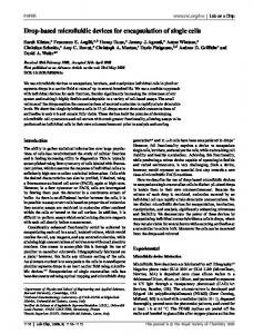
In Figure 1 a schematic representation is given for the development of black spots. In Fig. 1(a) there is a defect in the inorganic barrier layer, but because this defect does not coincide with the defect in the BaAl cathode it does not lead to the growth of a black spot in the OLED. On the right side the defect in the cathode is well covered by the inorganic barrier and will also not be the cause for the development of a black spot, provided that the intrinsic WVTR of the barrier is low enough, as addressed earlier. In Fig. 1(b) the defects in the inorganic barrier layer and the BaAl cathode are coupled and will therefore lead to the creation of a black spot which grows linear in time. In Fig. 1(c) the inorganic barrier is covered by an organic film, which has negligible intrinsic barrier properties. Therefore, the water can permeate through that layer and subsequently via the defect in the inorganic layer towards the interface between the organic semiconductor and the cathode. In Fig. 1(d) the cathode is covered by an inorganic-organic-inorganic barrier stack. This situation will still lead to the development of a black spot, but delayed in time. The delay time depends on the size of the defects, the distance between the two defects
5
and the properties of the interlayer. The time delay should be very significant, with an aim of more than 10 years, if the inorganic films have a low defect density.
In the experiments described in this article plasma enhanced ALD (PE-ALD) Al2O3 layers will be compared to state-of-the-art a-SiNx:H layers deposited by plasma enhanced chemical vapor deposition (PE-CVD), which is one of the most adopted inorganic barrier/ encapsulation layer. The intrinsic WVTR of the films were investigated by means of calcium test, and number and size of defects in the encapsulation were studied with the films applied directly on top of the OLED cathode. Film stacks of Al2O3 and a-SiNx:H, with and without the application of an organic layer in those stacks, are investigated for their influence on the defect density in the encapsulation.
II. Experimental A. Thin film barrier deposition The synthesis of the PE-ALD films has been carried out in a FlexAL reactor of Oxford Instruments. The ALD cycle was consisted of 4 steps: Al(CH3)3 (trimethylaluminum, TMA) dosing (20 ms), purge with O2 gas (1.5 s), O2 plasma (4 s), and purge with O2 gas (0.5 s). The O2 flow was constant throughout the whole cycle and only the TMA pulse was alternated as well as the plasma power.9 Since the organic semiconductor in the OLED cannot withstand temperatures higher than 110 oC the deposition temperatures for the barrier layers were restricted to 110 oC or lower. Because of this restriction PE-ALD was preferred over thermal ALD.8, 19,
20
All ALD layers presented here were deposited at
25 oC. The choice for deposition at room temperature was based on the results of our 6
earlier work by Langereis et al.21 The TMA, which was kept at 30 oC, was dosed vapor drawn using fast Swagelok ALD valves. The remotely placed inductively coupled plasma (ICP) source, was operated at 400 W. During the process the reactor was kept at a pressure of 15 mTorr. The resulting growth rate of this Al2O3 process was 0.17 nm per cycle. The material had a [O]/[Al] ratio of 1.88 and contained ~15 at.% hydrogen.19, 20 Both observations indicate the incorporation of a significant concentration of OH-groups which was also observed experimentally in a separate study.21 More detailed information about the reactor and the Al2O3 process can be found elsewhere.19
The a-SiNx:H films were deposited in a Plasmalab 800plus reactor of Oxford Instruments, which is a capacitively coupled parallel plate reactor driven at 13.56 MHz. For the deposition of a-SiNx:H, a plasma was generated in a SiH4/ N2/ NH3 mixture. For a substrate temperature of 110 oC this resulted in stress free (< 80 MPa) a-SiNx:H films with a hydrogen content of 20 - 30%. The deposition rate was 0.5 nm/s and the refractive index of the films was n = 1.90. More details about the performance of the a-SiNx:H films in barrier applications are reported elsewhere.4
A 20 m thick acrylate-based organic layer (Ixan-SGA-1 supplied by Solvay plastics) performed either as interlayer between two inorganic barriers or as top layer to improve the mechanical stability of the multi-stack. The organic material was brushed onto the sample and then left to dry. During this procedure the samples did not leave the glove box.
7
B. Sample description and analysis The intrinsic barrier performances have been evaluated by means of the calcium test.22 The experiments were carried out following the approach and methodology described by Nisato et al.23 The substrates were 150 x 150 mm glass plates covered by 40 nm Ca prepared by thermal evaporation. On top of the calcium 40 nm SiO2 was deposited by PE-CVD which served as temporary barrier against moisture permeation during sample transportation. The SiO2 layer has no influence on the measurements since its WVTR was measured to be in the order of 10-2 g·m-2·day-1, while the ALD Al2O3 and the PE-CVD aSiNx:H are three orders of magnitude better in terms of barrier performance, as will be discussed below. The Ca material has been deposited on the plates in a structure consisting of nine pads and each pad is divided in nine squares [see Fig. 2(a)], to avoid that the water vapor permeating through one defect would affect the whole area of the samples. When one of these squares showed a white spot (when Ca oxidizes it becomes transparent), as caused by a defect in the barrier film, that specific square was disregarded from the test. In such case the results of the rest of the squares were averaged to determine the intrinsic barrier performance of the inorganic layers. The Ca samples have been tested under 20 oC and 50% relative humidity (RH) conditions
The measurement setup for the calcium test (developed by Philips Research) consisted of a Philips CL5000M light source with a diffuser for uniform back lighting and a sample holder with mask. A 12 bit Adimex MX12p camera was used to obtain a gray scale image of the sample. The amount of oxidation is determined from the gray tint. A nontransparent black reference from the mask and a white reference from the transparent part
8
of the glass plate have been included in every measurement to set the gray scale range and to correct for transparency changes due to the barrier film. This setup has been calibrated by performing an experiment where the calcium samples were measured on this setup and by Rutherford backscattering (RBS) simultaneously, and thus relating the optical transmission through the sample to the [Ca]/[O] ratio in the samples. To obtain results with 10% precision the test should last until at least 1 nm of the Ca material has been oxidized. Since only the top 1 nm of metal Ca is oxidized in these experiments, it can be assumed that each H2O molecule reacts with one metal Ca atom to form CaO and that further oxidation to Ca(OH)2 does not occur yet.
In addition to the intrinsic barrier performance evaluation, the encapsulation of the local defects was studied by means of electroluminescence (EL) measurements carried out on OLEDs. These measurements have been performed at regular intervals in time to register the quantity and size of the resulting non-emissive black spots (see Fig. 2) as a function of time. For these experiments we have used OLEDs based on polymers. They have been synthesized on glass substrates of 150 x 150 mm and on each substrate 9 devices have been prepared, each device with an activated area of 6 cm2. Experiments were carried out on batches of 4 glass plates and to minimize effects of plate-to-plate variations, each barrier layer/stack was prepared on 9 OLED devices distributed over 3 plates. A BaAl layer (5 nm Ba and 100 nm Al) has been used as a cathode. A more extensive description of the OLED stack can be found elsewhere.24
9
After encapsulation the OLED samples have been stored for shelf lifetime testing at 20 oC and 50% RH. For the EL measurements the OLEDs were temporarily removed from their controlled environment, switched on, and photos of the powered devices under operational conditions were taken. This process was repeated on regular basis, i.e. every day and once every week at later stages of the test. The EL photos were analyzed by imaging software to count the number of non-emissive black spots per device and to calculate the area of every black spot at that time. The detection limit for the software to recognize a black spot was 1000 μm2.
For the black spot analysis we have used the following processing rules: a black spot is defined as visible when having an area larger than 0.01 mm2. To become visible within 10 years a black spot has to grow faster than 0.1 μm2/h, therefore all spots with a lower growth rate have been removed from the dataset. The application of this rule excluded for example the visible dust particles blocking the light and the defects that formed a black spot during processing but were encapsulated successfully by one of the layers higher in the stack. Furthermore, the imaging software took only circular black spots in a picture into account. This means that the size of a spot could no longer be calculated as soon as the spot merged with another spot or reached the edge of the OLED. In several cases this effect limited the number of data points for a black spot. Finally, all black spots with less than 4 data points have been excluded in order to filter out errors in the measurements caused by the analysis software. Because of these constraints in the analysis, it should be mentioned that a large scatter in the data is present, as will be addressed in Section III.
10
C. Sample handling Sample handling was an important part of these experiments and it is therefore described in detail below. The OLED and calcium samples were produced by Philips Research in a glove box. Attached to this glove box was the Oxford Instruments Plasmalab 800plus tool which was used for the a-SiNx:H and SiO2 synthesis. For the deposition of the Al2O3 films the samples had to be transported to the Eindhoven University of Technology (TU/e) with a travel time of approximately 30 minutes. The samples were transported together with Ca getter material in a box under N2 atmosphere. After arrival at the TU/e the transport box and samples were immediately introduced into a glove box. In an exsiccator the samples were brought to the FlexAL reactor located in the TU/e clean room, where they were loaded through open air. After deposition the samples were placed back into the exsiccator, which was then evacuated and returned to the glove box. When all samples had been processed they were returned to Philips Research for further processing or to start the sample analysis.
III. RESULTS AND DISCUSSION A. Water vapor permeation through single layer barriers The importance to distinguish between intrinsic WVTR (water vapor permeation through the film in regions far from defects) and defects in the film has been stressed in the Introduction. In Fig. 3 a comparison is shown between the intrinsic WVTR values of the PE-ALD Al2O3, and the PE-CVD a-SiNx:H films. For Al2O3, data is given for 20 and 40 nm thick films while the thickness of the a-SiNx:H film was 300 nm. The test lasted
11
for 70 days at 20 oC/ 50% RH condition, before it had to be stopped since too many samples showed white spots indicating defects in the encapsulation. Over this period of time only 0.5 nm of Ca had been oxidized, which means that all layers that were subject to this test had an intrinsic WVTR in the 10-6 g·m-2·day-1 range that is required for OLED encapsulation. Remarkable is that although the PE-ALD Al2O3 films are one order of magnitude smaller, they still show the same performance as the PE-CVD a-SiNx:H films. Since the 20 and 40 nm Al2O3 films show a similar WVTR value, we can conclude that thicker layers for the ALD Al2O3 will not result in any further improvement of barrier properties.
ALD Al2O3 layers have been evaluated in terms of WVTR earlier in the literature.10, 15, 16, 25, 26
However, differences in test methods and testing conditions hamper a direct
comparison, even in cases when similar Ca tests have been performed. For example, both Meyer et al.25 and Carcia et al.26 conclude that their Al2O3 barrier films, which are synthesized by thermal ALD on polymer substrates, can reach values in the order of 10-6 g·m-2·day-1 at room temperature conditions. This confirms our results, however the best WVTR values reported by Meyer et al. were 3.5·10-4 g·m-2·day-1, measured at 70 oC/ 70% RH conditions for 100 nm thick films. Carcia et al. have reported a WVTR of 1.7·10-5 g·m-2·day-1 under 38 oC/ 85% RH conditions for 25 nm thick films, but indicated that their test values were limited by the epoxy which they used to glue the samples to the Ca substrates.
12
B. Single layer encapsulation of OLED devices Since it has been shown that thin ALD Al2O3 films do meet the requirement as barrier layer for OLED encapsulation in terms of intrinsic WVTR properties, the focus was shifted towards the size and density of defects and their encapsulation by the single layers. In Fig. 4 the results for single layer Al2O3 films have been compared with those for the a-SiNx:H film in terms of number of black spots per device and the average black spot growth rate. From the number of black spots, it can be concluded that the 20 and 40 nm ALD Al2O3 layers can effectively encapsulate the defects present on the cathode surface. They show better results than the a-SiNx:H reference, which is likely due to the higher conformality that is typical for films synthesized by ALD.
The average growth rate of the black spots is also reported in Fig. 4. The ALD layers exhibit in general a higher black spot growth rate and this might indicate that the ALD encapsulation mechanism is mainly efficient for the small defects present at the surface. The ALD layer can leave the largest defects either uncovered or the layer itself could suffer from local stress around the large defects, therefore promoting an easier permeation path for water vapor to diffuse through the barrier layer. The thicker a-SiNx:H layer appears to perform better in terms of encapsulation of larger defects, which can be the results of the synergic combination of a larger thickness and a locally reduced stress. The comparison between the ALD Al2O3 layers of 20 and 40 nm showed that the devices encapsulated with 20 nm films leaves more defects uncovered and, on the basis of this result, the deposition of the stacks (see Sec. III.C) has been carried out only with the 40 nm thick ALD Al2O3 films.
13
A large scatter has been found in the growth rate data and the error bars were estimated to be as large as the measured values. From previous experiments we have learned that the number of particles can vary from batch to batch (a batch is a series of 4 glass plates, each with 9 OLEDs) and even from plate to plate, which is the main reason for the scatter in the data. We note therefore that we only compared samples within one batch in order to limit the spread in particle density. To cancel the effects of the plate-to-plate variation each barrier has been prepared on 9 OLEDs distributed over 3 plates as discussed in Sec. II. When the number of defects in the barriers became low due to the improvement of the encapsulation it became more challenging to get statistics from the experiments.
C. Film stacks for OLED encapsulation To investigate the impact of the stacks on the OLED performance in terms of defect encapsulation, several stacks were prepared and compared. In these stacks the inorganic Al2O3 (40 nm) and a-SiNx:H (300 nm) layers were included, and an acrylate-based organic layer was introduced as well. This organic layer had negligible barrier properties but it served as mechanical protection of the device when applied as top layer. It could also generate a delay in water vapor permeation when applied as interlayer between inorganic layers (see Introduction).
As already shown in Fig. 4, a stack of a-SiNx:H and Al2O3 (Al2O3 on top) neither reduced the number of black spots to a significant extent, nor significantly affected the growth rate of the black spots. Therefore in Fig. 5 a more extensive comparison has been made
14
between various stack structures in terms of average number of black spots focusing on the case where the Al2O3 was applied first. With an average of only 3.6 black spots per device (active area is 6 cm2) the a-SiNx:H encapsulation in this specific batch of OLEDs performed extremely well. Usually, the a-SiNx:H barrier has between 10 and 15 black spots per OLED, as shown in Fig. 4. This quality of the a-SiNx:H encapsulation was not reproduced in any of the other batches. Although the a-SiNx:H film was of exceptional quality, applying first a 40 nm ALD Al2O3 layer on the cathode reduced the average number of defects by a factor of two (see Fig. 5, right side). Expanding the Al2O3 and a-SiNx:H film stack with extra layers decreased the amount of pinholes even further. This was best evidenced by results obtained for an Al2O3/ a-SiNx:H/ Al2O3/ organic stack. This stack revealed an average of only 0.7 black spots per OLED, which corresponds to 0.12 black spots per cm2. The beneficial effect of stacking ALD Al2O3 and PE-CVD a-SiNx:H layers have been reported before by Carcia et al.,10 but they indicated that their test values were limited by the epoxy which they used to glue the samples to the calcium substrates.
We note that the application of an organic layer on top of this stack structure did not have a beneficial effect, as can be concluded from the comparison between the single a-SiNx:H layer and the a-SiNx:H covered by the organic layer (see Fig. 5, left side). However, when the organic layer was applied as interlayer between a-SiNx:H layers (i.e. a-SiNx:H/ organic/ a-SiNx:H), it did show a decrease in the amount of black spots. This reduction can be attributed to the decoupling of the defects in the two inorganic layers leading to a time delay in the appearance of black spots during the electroluminescence
15
measurements. In this case the delay was large enough such that fewer black spots appeared in the timeframe of the measurement. This is therefore also considered a promising approach that can also be pursued for ALD Al2O3 as inorganic layer. Similar positive effects of building a barrier stack of inorganic and organic layers have been discussed in several articles,18, 27, 28 but few authors report on barrier films deposited directly on the cathode of the OLEDs.4, 24
IV. CONCLUSIONS The water vapor permeation barrier properties of 20 and 40 nm thick Al2O3 films prepared by PE-ALD have been investigated with respect to the encapsulation of OLED devices and compared to a 300 nm thick PE-CVD a-SiNx:H film as reference. Both layers revealed an excellent intrinsic WVTR in the range of 10-6 g·m-2·day-1. However, with a WVTR of 2·10-6 g·m-2·day-1 the PE-ALD layers outperformed the PE-CVD a-SiNx:H, particularly considering the one order of magnitude smaller film thickness of the Al2O3 layers.
The encapsulation of defects present at the cathode surface of the OLED has also been investigated for both materials. The OLED encapsulated by PE-ALD Al2O3 films showed on average 3-4 black spots per device on a 6 cm2 active area, which was 4 times lower than the devices encapsulated by PE-CVD a-SiNx:H films. This result is remarkable considering that the PE-ALD layers are much thinner than the PE-CVD a-SiNx:H films. It demonstrates that the ALD layer is beneficial for the encapsulation of particles present on the cathode of an OLED, most likely due to the 3D conformal growth of the ALD films.
16
By stacking the inorganic barrier films we have shown that it is possible to reduce the number of defects in the encapsulation even further. The best result in our experiments was a defect density of 0.12 defects per cm2, which has been obtained for barriers with three inorganic layers (Al2O3/ a-SiNx:H/ Al2O3) and an organic layer on top. From other experiments it was found that the organic layer as top layer did not improve the encapsulation, which means that the reduction of the number of defects can be fully attributed to the inorganic layers in the stack. By adopting the organic layer as interlayer between inorganic layers prepared by ALD, it is expected that defect encapsulation and defect decoupling can effectively be combined and therefore be the key to a defect free barrier.
Acknowledgements This work was funded by the Netherlands Technology Foundation STW. The OLED samples were processed by T. Bernards and his crew in the Philips MiPlaza OLED prepilot line. The black spot measurements were performed by M. Meulendijk in the Reliability Centre of Philips MiPlaza, supervised by M. Kuilder. The experimental and technical support by dr. E. Langereis and J.J.A. Zeebregts are gratefully acknowledged.
17
References 1
P. E. Burrows, G. L. Graff, M. E. Gross, P. M. Martin, M. K. Shi, M. Hall, E. Mast, C. Bonham, W. Bennett, and M. B. Sullivan, Displays, 22, 65 (2001).
2
F. J. H. van Assche, R. T. Vangheluwe, J. W. C. Maes, W. S. Mischke, M. D. Bijker, F. C. Dings, M. F. J. Evers, W. M. M. Kessels, and M. C. M. van de Sanden, Proc. Soc. Inf. Displays, 695 (2004).
3
J. S. Lewis and M. S. Weaver, IEEE J. Sel. Top. Quantum Electron., 10, 1 (2004).
4
A. M. B. van Mol, P. van de Weijer, and C. Tanase, Proc. SPIE, 6999, 46 (2008).
5
C. W. T. Bulle-Lieuwma and P. van de Weijer, Appl. Surf. Sci., 252, 6597 (2006).
6
J. H. Burroughes, D. D. C. Bradley, A. R. Brown, R. N. Marks, K. Mackay, R. H. Friend, P. L. Burns, and A. B. Holmes, Nature, 347, 539 (1990).
7
S. M. George, Chem. Rev., 110, 111 (2010).
8
H.B. Profijt, S. E. Potts, M. C. M. van de Sanden, and W. M. M. Kessels, J. Vac. Sci. Technol. A, 29, 050801 (2011).
9
S. B. S. Heil, J. L. van Hemmen, M. C. M. van de Sanden, and W. M. M. Kessels, J. Appl. Phys., 103, 103302 (2008).
10
P. F. Carcia, R. S. McLean, M. D. Groner, A. A. Dameron, and S. M. George, J. Appl. Phys., 106, 023533 (2009).
11
A. A. Dameron, S. D. Davidson, B. B. Burton, P. F. Carcia, R. S. McLean, and S. M. George, J. Phys. Chem. C, 112, 4573 (2008).
12
E. Langereis, M. Creatore, S. B. S. Heil, M. C. M. Van de Sanden, and W. M. M. Kessels, Appl. Phys. Lett., 89, 081915 (2006).
18
13
A. P. Ghosh, L. J. Gerenser, C. M. Jarman, and J. E. Fornalik, Appl. Phys. Lett., 86, 223503 (2005).
14
J. Meyer, D. Schneidenbach, T. Winkler, S. Hamwi, T. Weimann, P. Hinze, S. Ammermann, H. -H. Johannes, T. Riedl, and W. Kowalsky, Appl. Phys. Lett., 94, 233305 (2009).
15
M. D. Groner, S. M. George, R. S. McLean, and P. F. Carcia, Appl. Phys. Lett., 88, 051907 (2006).
16
S. H. K. Park, J. Oh, C. S. Hwang, J. I. Lee, Y. S. Yang, and H. Y. Chu, Electrochem. Solid-State Let., 8, H21 (2005).
17
C. Y. Chang, C. T. Chou, Y. J. Lee, M. J. Chen, and F. Y. Tsai, Org. Electron., 10, 1300 (2009).
18
G. L. Graff, R. E. Williford, and P. E. Burrows, J. Appl. Phys., 96, 1840 (2004).
19
J. L. van Hemmen, S. B. S. Heil, J. H. Klootwijk, F. Roozeboom, C. J. Hodson, M. C. M. van de Sanden, and W. M. M. Kessels, J. Electrochem. Soc., 154, G165 (2007).
20
S. E. Potts, W. Keuning, E. Langereis, G. Dingemans, M. C. M. van de Sanden, and W. M. M. Kessels, J. Electrochem. Soc., 157, P66 (2010).
21
E. Langereis, J. Keijmel, M. C. M. van de Sanden, and W. M. M. Kessels, Appl. Phys. Lett., 92, 231904 (2008).
22
G. Nisato, P. Bouten, P. Slikkerveer, W. Bennett, G. Graf, N. Rutherford, and L. Wiese, Proc. Asia Display, 1435 (2001).
23
G. Nisato, M. Kuilder, P. Bouten, L. Moro, O. Philips, and N. Rutherford, SID Int. Symp. Dig. Tec., 34, 550 (2003).
19
24
P. van de Weijer, G. Rietjens, C. Tanase, H. Lifka, J. Michels, F. J. H. van Assche, and T. van Mol, Proc. OSC, (2008).
25
J. Meyer, P. Görrn, F. Bertram, S. Hamwi, T. Winkler, H.-H. Johannes, T. Weimann, P. Hinze, T. Riedl, and W. Kowalsky, Adv. Mater., 21, 1845 (2009).
26
P. F. Carcia, R. S. McLean, M. H. Reilly, M. D. Groner, and S. M. George, Appl. Phys. Lett., 89, 031915 (2006).
27
M. Schaepkens, T. W. Kim, A. G. Erlat, M. Yan, K. W. Flanagan, C. M. Heller, and P. A. McConnellee, J. Vac. Sci. Technol. A, 22, 1716 (2004).
28
T. W. Kim, M. Yan, A. G. Erlat, P. A. McConnelee, M. Pellow, J. Deluca, T. P. Feist, A. R. Duggal, and M. Schaepkens, J. Vac. Sci. Technol. A, 23, 971 (2005).
20
Figure captions Fig. 1: Schematic representation of water vapor permeation through defects in the encapsulation layer. (a) Successful encapsulation (under the hypothesis of an intrinsic barrier value of 10-6 g·m-2·day-1). The defect in the inorganic layer will not lead to black spots, while the defect in the cathode is well encapsulated. (b) A defect in the cathode propagates in the inorganic layer such that the water can reach the interface between the cathode and the organic semiconductor and cause a black spot. (c) Because the organic layer has no barrier properties, this case leads to a similar problem as in (b). (d) Defects are decoupled by an organic layer and the path length of water to reach the interface between the cathode and the organic semiconductor through the organic layer determines the time delay before the initiation of the black spot.
Fig. 2: Photos of the a) calcium sample, and b) OLED during electroluminescence measurements. The white spots on the calcium sample and the black spots on the OLED are due to water vapor permeation through defects in the encapsulation layer.
Fig. 3: The intrinsic water vapor transmission rates (WVTR) measured for 300 nm a-SiNx:H deposited by PE-CVD, 20 and 40 nm PE-ALD Al2O3. The layers have been deposited directly on the SiO2 -covered calcium sample. The shelf lifetime has been tested at 20 oC/ 50% RH and lasted for 70 days.
Fig. 4: (a) The average number of black spots per OLED, and (b) the average growth rates per black spot as measured by electroluminescence on OLED samples encapsulated
21
with 300 nm a-SiNx:H, 40 nm and 20 nm Al2O3. Results for a stack of a-SiNx:H (300 nm) and Al2O3 (40 nm) are given as well. The barrier films have been deposited on the cathode of the OLED. The samples have been kept at 20 oC/ 50% RH for 114 days and have only been removed to perform the electroluminescence measurements. The error bars for the average growth rates are estimated to be ~100% of the measured value.
Fig. 5: The average number of defects per OLED for several stacks that combine 300 nm of a-SiNx:H deposited by PE-CVD, 40 nm Al2O3 prepared by PE-ALD, and organic (org.) layers. The samples have been kept at 20 oC/ 50% RH for 158 days and have only been removed to perform the electroluminescence measurements.
22
List of Figures (a)
(b)
(c)
organic inorganic BaAl cathode OLED
(d) Figure 1
23
(a)
(b)
Figure 2
24
Figure 3
25
Figure 4
26
Figure 5
27