[21] Kenneth S. Stevens, Shai Rotem, Steven M. Burns, Jordi Cortadella, Ran. Ginosar ... stages. In Peter Kornerup and David W. Matula, editors, Proceedings.
Characterization of Asynchronous Templates for Integration into Clocked CAD Flows Kenneth S. Stevens, Yang Xu, and Vikas Vij Electrical and Computer Engineering University of Utah
Abstract—Asynchronous circuit design can result in substantial benefits of reduced power, improved performance, and high modularity. However, asynchronous design styles are largely incompatible with clocked CAD, which has prevented wide-scale adoption. The key incompatibility is timing. Thus most commercial work relies on custom CAD or untimed delay-insensitive design methodologies. This paper proposes a new methodology, based on formal verification and relative timing, to create and prove correct necessary constraints to support asynchronous design with traditional clocked CAD. These constraints support timing driven synthesis, place and route, and behavior and timing validation of fully asynchronous designs using traditional clocked CAD flows. This flow is demonstrated through a simple example pipeline in IBM’s 65nm process showing the ability to retarget the design for improved power and performance.
and can be used by designers trained in clocked methodologies. We view the difference in timing methodologies as the primary impediment to exploiting traditional clocked CAD and implementing handshake clocked designs. This paper reports on a methodology, based on formal verification and relative timing, that supports timing driven synthesis, physical design, and pre- and post-layout timing validation of handshake clocked designs using traditional clocked CAD. This approach enables the general adoption of asynchronous or “handshake clocked” circuits in the traditional clocked flow. This new flow consists of fully characterizing the asynchronous handshake clocking circuits as design templates that replace the clock tree in a traditional clock design.
I. I NTRODUCTION Two factors have driven a major shift in the semiconductor industry as a result of the ever decreasing feature size of deep submicron technology. First, power has emerged as a primary metric for all designs, whether they are are hand held devices or desktop machines. Second, the exponential increase in the number and performance of transistors on our chips has grown to the point where modularity and design reuse is mandatory, and efficient global synchronous clocking throughout the chip is expensive in terms power and design time. Modular design blocks are easier to integrate, and can be more power efficient if they operate at variable or local optimums using independent frequencies. Current trends clearly favor asynchronous design: networks of heterogeneous cores that are locally optimized for power and cycle time. Due to these factors the International Technology Roadmap for Semiconductors predicts that 20% of designs will be driven by handshake clocking in 2012, rising to 40% by 2020 [16]. Example designs that employ such methods have shown substantial improvements in power, performance, and latency [23], [18]. Handshake clocking relies on asynchronous controllers to sequence a traditional “clocked” data pipeline. The formal handshake protocols provide the requisite flexibility in frequency and simplicity of modular interfacing. Unfortunately, integrating handshake clocking with traditional clocked data pipelines has proven problematic [10], [21]. In practice, the radical and disruptive paradigm shift to fully asynchronous design has been unsuccessfully attempted for years. General adoption as predicted in the ITRS will be unlikely to occur without a new approach that supports traditional CAD flows
II. BACKGROUND A. Related Work The path to general adoption of a disruptive technology such as asynchronous circuit design is fraught with difficulty and challenge. One of the primary roadblocks is the CAD flow [21], [10]. This poses three problems for asynchronous design. First, clocked CAD flows are in general incompatible with sequential asynchronous design. Second, clocked CAD tools are in general more capable than their asynchronous cousins. Third, there is a general level of distrust in the ability to correctly and robustly design commercial asynchronous circuits. The ability to adapt clocked CAD and design flows to asynchronous design, and to base asynchronous designs on formal proofs of correctness, are enabling approaches that can greatly mitigate the adoption of asynchronous circuits by the general design community. Recent research in the asynchronous community has begun to achieve more industrial acceptance and broader use of asynchronous designs by focusing on addressing the CAD challenge. This has been achieved by integrating and adopting clocked CAD where advantageous. The goals of this work are no different. However, this work stands out from the rest on two primary fronts. First, the methods used in this approach are completely general to any asynchronous design, and applies to bundled data as well as delay-insensitive designs; to any protocol, be it two or four phase, dual rail, or single track; and to any design flow, including a desynchronization approach or full custom asynchronous design. Second, this approach is not beholden to a programming language; we assume adoption of today’s de facto standard of Verilog.
Related work that is probably the most technologically advanced and commercially successful comes from Handshake Solutions [12]. A complete synthesis, layout, and sign-off solution for both Cadence and Synopsys based design flows has been developed [6], and includes support for automatic test generation [22]. Constraints and scripts from a higher level language are generated that are supported by the clocked CAD. Unfortunately there is little public documentation on the algorithms or design methodology used to generate the constraints and implement this flow. The flow is also tightly coupled with their proprietary programming language. Another commercial tool flow based on clocked CAD is from Theseus Logic [5], [9]. This flow supports Verilog design descriptions and translates the design to quasi delay-insensitive null convention logic [8]. The Theseus flow does not directly support bundled-data or other asynchronous methodologies. Desynchronization is another design approach that uses clocked CAD (as well as starting with a clocked design) to produce asynchronous circuits [4], [1]. There are a number of current research and industrial efforts focusing on this promising flow. Desynchronization supports Verilog and uses a template based approach, and algorithms have been developed for test generation [14]. However, this flow does not support general asynchronous design, largely due to the low number of asynchronous templates and custom tools. There are several other related research efforts to utilize clocked CAD. In one example, an automated method was developed for interconnect network, but it does not support matching delays and bundled data [13]. B. Generally Applicability A key difference between the approach presented here and other work is the generality of the solutions. This work supports designs from clocked, to standard asynchronous protocols, to pulse based [15], to wave pipelining designs [24]. This technology enables asynchronous designs to be specified in industry standard representations such as Verilog, supports synthesis with ASIC tools such as Design Compiler, uses timing driven place and route tools such as IC Compiler or Magma, and can be validated for correctness using Calibre and PrimeTime. This new method when mature will not require deep expertise in asynchronous theory or circuits design skills. Desynchronization is an example of an approach to develop handshake clocked designs [4], [1]. The method presented in this paper supports desynchronization but is not limited to such a methodology; indeed it can be applied to any asynchronous design. The key to the generality is the formal approach. Formal verification (FV) is orthogonal to any particular synthesis engine or design style. Thus all timing methodologies, from clocked to delay insensitive (DI), are supported. Hence this methodology frees designers from the constraints of any asynchronous design style (e.g. DI) or custom design tool flows. The verification utilizes relative timing (RT), which also supports all classes of timing, from clocked to fully DI [20]. This is implemented as follows. Each sequential template (clocked
clki 7→ data ≺ clki+1 +m |{z}
|
{z
}
timing assumptions spec. design
? r- RT-FV
absolute margins
? RT constr. - STA
- signoff
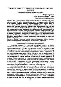
6 initial conditions Fig. 1. Formal Relative Timing Generation and Mapping to static timing analysis (STA) Tools
or asynchronous) starts with a formal specification. The timing constraints that must hold, be they quasi delay-insensitive forks or matched bundled data delays, are all formally derived as relative timing constraints. These RT constraints are proven correct for the system behavior by the specification. The RT constraints are then mapped to constraints that the clocked CAD can use for timing driven design optimizations (typically sdc constraints). This results in a design that is completely general and provably correct if all the constraints hold. The proposed asynchronous design flow is similar to the traditional clocked design flow. Clocked design has focused its design methodology around a single characterized sequential circuit: the flip-flop. This work extends design to directly support any sequential or asynchronous module in the design flow. The asynchronous design modules, such as the flop, will be embodied in circuit templates that have been fully characterized with FV and relative timing, and can support handshake clocking protocols as well as global clocking. These templates are then used in the design. While relative timing is the foundation of this approach giving it formal robustness and flexibility, other algorithms are necessary to completely automate this flow. Algorithms to support the templates in ASIC CAD include cycle breaking to apply timing graphs that are DAGs, synthesis directives to ensure the hazard properties of the templates are not modified, and conversion of the template timing constraints into sdc format for support by ASIC tools. Templates will be designed that support the conversion of clocked design into asynchronous “handshake clocking”. This full flow will be presented through the simple example design. C. Formal Timing and Verification Relative timing can accurately capture, model, and validate the relationship between heterogeneous timing and behavior in protocols and general circuit structures, including sequential asynchronous designs. First, timing constraints are made explicit in designs, rather than use the traditional implicit representations such as a clock frequency. This allows designers and tools to specify, understand implications, and manipulate the timing of far more general circuit structures and advanced clocking techniques. Secondly, timing constraints that affect
A binary relation LC ⊆ P × P over agents is a logic conformation between implementation I and specification S if (I, S) ∈ LC then ∀ α ∈ Act and ∀ β ∈ A ∪ {τ } (outputs and τ ) and ∀ γ ∈ A (inputs) α (i) Whenever S →S 0 then
b α
∃ I 0 such that I ⇒I 0 and (I 0 , S 0 ) ∈ LC β
(ii)
Whenever I →I 0 then
(iii)
∃ S 0 such that S ⇒S 0 and (I 0 , S 0 ) ∈ LC γ γ Whenever I →I 0 and S ⇒ then γ ∃ S 0 such that S ⇒S 0 and (I 0 , S 0 ) ∈ LC
β
b
Fig. 2.
Bisimilar Logic Conformance Relationship
the performance and correctness of a circuit are transformed into logical constraints, rather than into real-valued variables or delay ranges. A compact representation has been developed using point-of-divergence (POD) to point-of-convergence (POD) constraints. The POD/POC (pod 7→ poc0 ≺ poc1 ) representation enables more efficient search and verification algorithms to be developed which greatly enhances the ability to combine timing with optimization, physical placement, and validation design tools [17]. This approach alters the way in which timing is represented by designers and CAD tools, and has been shown to provide significant power-performance advantages in some circuit designs [18], [20]. Formal verification and relative timing is the key technology that permits templates to be characterized in a way that is compatible with clocked CAD. The formal verification uses model checking. The representation and method of generating RT constraints is shown in Fig. 1. This work applies a conformance relation between the specification (spec.) and implementation (design) based on the bisimulation conformance relation shown in Fig. 2. The formal verification tool (RT-FV) proves correctness of an implementation against a specification. Timing constraints are represented as logical expressions that make error states unreachable. A set of constraints can be automatically generated that restrict the timing of the implementation such that it conforms to the specification [7]. Now timing is fully represented in the logical and behavioral domain. The constraints are then mapped to a format acceptable by a static timing analysis (STA) engine, synthesis engine, or place and route engine, such as PrimeTime, Design Compiler, or SoC encounter. D. Template Based Methodology Rather than compete in the CAD domain and develop fully independent flows, one can apply commercial clocked CAD and its associated algorithms as broadly as possible, and restrict custom tools to the necessary asynchronous circuit and verification problems. This approach, unlike purely asynchronous design, is able to leverage the significant industrial investment in synchronous design tools. Such a flow is supported in this paper based on “design templates” which are the asynchronous sequential components of a design. If this approach is successful and adopted by industry, designers will be able to build asynchronous systems based on the merits of
the architecture, such as performance and power. This approach to asynchronous design with clocked tools thus has two facets: (a) the design and characterization of the asynchronous templates, and (b) traditional system design that employs the asynchronous templates. The key to making this happen is to develop characterized templates that can be manipulated and optimized when inserted into the clocked CAD flows. The design and characterization of the asynchronous templates requires substantial expertise in asynchronous design and verification. However, once the templates have been completed, they can be inserted into a design flow by clocked designers with little expertise in asynchronous design. Thus a bulk of the asynchronous circuit and CAD are restricted to off-line library design and characterization. III. F ORMAL C HARACTERIZATION F LOW The characterization of an asynchronous template is somewhat complicated, and will be demonstrated on the design of a linear pipeline controller LC. This template is part of a simple design example shown in Fig. 3 that will be used in the remainder of this paper. There are only two asynchronous templates in this design, the linear controller (LC) and the Fork Join template (F/J). The rest of the design is synthesized using normal clocked tool flows. We have designed a small microprocessor using this flow, and this example is a conceptual piece of such a design that calculates the function x2 + 3x. A. Bundled Data with Clocked Datapath Bundled data asynchronous designs are partitioned into two signal classes: the datapath and control. The datapath in Fig. 3 consist of the registers (R) and oval boxes implementing arithmetic functions. The registers are implemented as either latches or flip-flops. This datapath is synthesized using Design Compiler based on frequency parameters provided by the user. The rest of the design is the control logic – which is implemented by the clock distribution logic in clocked design. To create a “handshake clocked” design, the global clock is replaced with the control logic. In this case there are four instantiations of the linear controller (LC) and two of the fork join (F/J) module. The responsibility of the handshake clocking is to maintain the timing and functional relationship between data in adjacent pipeline stages, implementing stalls when necessary. This is achieved by implementing a handshake protocol in the LC blocks. Extra delay may be needed between the control blocks so that the clock signal does not arrive at the flop before the input data is valid. Hence a matched delay will be implemented between the data banks i and i + 1 on the control path. For example, the delay from r0 to r00 must match the x2 datapath from R0 q to the input of R10 . B. Asynchronous Template Design Numerous handshake protocols and asynchronous circuit designs are feasible realizations for linear pipelines. The protocol and circuit design for each template will have a large impact on the design in three ways. First, the templates directly
�
� 2
� x-
din
R0
R0
q
16
ck
- lr la
�
rr
LC0
ra
r0 a0
s
F/J0
q
�
32 ck10
r00 a00
ck0 lr la
R10
R10
x
�
� �
R11
R2
- dout ck2
32
F/J1
R11
3x
�
+
r10 a10
�
�
rst
LC10
�
r1 a1
LC2 �
- rr ra
q
�
ck11 r01 a01
Fig. 3.
lr
r
r
ra
HH cra r r �� Fig. 4.
r11 a11
Example design: a simple ASIC mathematical pipeline segment computing dout = x2 + 3x
r
LC11
clar HH c r r la ��
HH c - ck � � � y c C �
crr
c r r - rr
rst
= = =
LEFT RIGHT SPEC
Fig. 5.
� x
lr.c1.la.c2.lr.la.LEFT c1.rr.c2.ra.rr.ra.RIGHT (LEFT | RIGHT) \{ c1, c2 } CCS specification of linear controller
la↑
� � ? PP �� x ra↓ x P� �� P � PP �� P � q P ? ) ? rr↑
lr↓
? �
la↓
?
lr↑
� ?P
j
? ra↑
LC circuit implementation
impact the performance and power based on the complexity of the design and the concurrency of the protocol. Second, the characterization of the template critically depends on the protocol and implementation. Finally, the correctness of the system, particularly with cyclic pipelines, will depend on the protocols and storage elements employed [2]. Hence our method supports all templates. The design used for the linear controller in this example is shown in Fig. 4. This implements the four-cycle return to zero handshake protocol shown in Fig. 5 and 6 as CCS and Petri-Net specifications [11], [3]. Our CAD tools support both representations. Note that this is a timed protocol (the dashed arcs in Fig. 6 constrain inputs), similar to a burst-mode specification. Such a protocol is chosen for this example because it illustrates the requirement of additional fundamental mode timing constraints to guarantee correct implementation in a design, as compared to delay-insensitive or speed-independent designs. The result of mapping this design to a Verilog module in the Artisan 65nm IBM 10sf library is shown in Fig. 7.
Fig. 6.
? rr↓
Petri net specification of linear control
C. Clocked CAD Tool Constraints Following are the sdc constraints supported by commercial tools that are used in this asynchronous template characterization. All of these commands affect the timing and power of the design. 1) set size only 2) set dont touch 3) set data check 4) set max delay 5) set min delay 6) set disable timing Structural modifications to a design may occur during synthesis and place and route flows. These changes result in optimizations such as removing back-to-back inverters, combining simple gates into a single complex gate, or breaking
module linear control (lr, la, rr, ra, ck, rst); input lr, ra, rst; output la, rr, ck; INVX1A12TH lc0 (.A(ra), .Y(ra )); AOI32X1A12TH lc1 (.A0(lr), .A1(ra ), .A2(y ), .B0(lr), .B1(la), .Y(la )); INVX1A12TH lc2 (.A(la ), .Y(la)); AOI32X1A12TH lc3 (.A0(ra ), .A1(lr), .A2(y ), .B0(ra ), .B1(rr), .Y(rr )); NOR2X1A12TH lc4 (.A(rr ), .B(rst), .Y(rr)); c element lc5 (.A(la), .B(rr), .Y(y )); INVX1A12TH lc6 (.A(la ), .Y(ck)); endmodule // linear control Fig. 7.
set set set set
size size size size
only only only only
-all -all -all -all
instances instances instances instances
{ { { {
*/lc1 */lc3 */lc4 */lc5
} } } }
Fig. 8. Size only constraints for the circuit of Fig. 7
Verilog implementation in the 65nm Artisan library
a complex gate into a set of simpler gates. Constraints are used to prevent this from occurring in the asynchronous blocks, because it could result in hazards or substantially modify necessary delay properties of the circuit. The set size only constraint prevents the tool from structurally modifying the cell but allows the tools to optimize the drive strength of the cell for power and delay optimization. The set dont touch constraint disallows the tool from modifying the cell in any manner. These commands take as arguments the cell instance names. The following command disallows structural modification of all lc3 instances (the AOI gate) in the example design. set_size_only -all_instances { */lc3 }
Traditionally the tools use clock domains to optimize circuits for power and performance. They understand setup and hold constraints into flops and latches. When the sequentials are driven from a simple clock domain the tools can optimize the combinational logic for the desired frequency. All of these tools operate on directed acyclic graphs, or DAGs. If the timing graphs have cycles, algorithms in the CAD tools are called to break the cycles. A user can manually define how to break the timing graphs with the set disable timing constraint. This will remove timing arc from a primitive gate (such as a NAND gate) from the specified input to the specified output. By removing the timing arcs in the primitive gates a manual instance of the timing graph, and how signals propagate through the circuit, can be defined. This is essential for sequential circuits that use handshaking since they always consist of cyclical timing paths. This command takes a -from pin name, a -to pin name and a list of cells. The following sdc command disables the timing arc from y to rr through one of the AOI gates in all instantiations of the linear controller in the example design. set_disable_timing -from A2 -to Y \ [find -hier cell *lc3]
By default, the maximum and minimum path delays are calculated by considering the clock edge times. Extensions to this flow have been implemented in the tools to override timing values, support asynchronous signaling, and timing domains that are not part of a fixed clock domain. These are the set max delay, set min delay, and set data check commands. One can override the timing constraints in a clocked domain with a specific time value by using the set max delay or
A� �A @ setup @ R
Fig. 9.
A� �A �
hold
� �
A A
constrained “to” signal
related “from” signal
The set data check command
set min delay command. This command has the side effect of breaking the timing graph at the two end points of the constraint (similar to the set disable timing constraint). This command has several options, but basically takes a -from set of path start points, a -through set of points the path must pass through, and a -to set of path end points, and the target delay value. Relative timing constraints can be checked using a pair of commands as follows. set_max_delay 1.7 -from [get_pins R0_reg_latch*/Q] \ -to [get_pins R10_reg_latch*/D] set_min_delay 1.7 -rise_from [get_clocks tk0/lr] \ -rise_to [get_pins tk10_lc1/A0]
The first constraint will make all the paths from the output of register R0 to the input of register R10 have a maximum delay of 1.7ns in our example design. The second will constrain the minimum delay path on the control path to also be 1.7ns. This path is from the lr input of the controller associated with register R0 to the input of the linear controller that clocks register R10. The set data check command is used to check setup or hold constraints between two unclocked data signals. The -from signal is considered to be the “clock” signal (called related) and the -to signal is considered to be data signal (called the constrained signal). This performs a the setup check and can be given a margin. This is clarified in Fig. 9. Given a relative timing constraint, the relative ordering of two signals can be mapped into -from and -to constraints with a slack time. The common point of divergence can be given with the -clock command, as shown: set_data_check -clock [get_clocks tk0/lr] \ -fall_from [get_pins tk0_lc3/A2] \ -rise_to [get_pins tk0_lc3/B1] -setup 0.05
This example implements the constraint lr↑ 7→ rr↑ ≺ lr↓ where lr↑ is the POD specified by -clock, rr↑ is the -rise to signal, and lr↓ is the -fall from signal. This command correctly
checks the maximum delay for the constrained -rise to signal against the minimum delay for the related -fall from signal, with a margin of 50ps. The combination of constraints allow us to utilize the synthesis, place and route, and timing tools to optimize and validate the timing of asynchronous designs D. Template Characterization This section describes the detailed flow required to characterized the LC pipeline template. 1) Model Generation: The first step in template characterization is converting the Verilog module (Fig. 7) into an equivalent formal representation for verification by model checking. This transformation is automated to aid in correctness and productivity. The CAD tool takes three inputs: (i) the Verilog design of the template, (ii) a mapping of Verilog gates to formal semi-modular description of each gate in CCS, and (iii) a functional description of the gates in the target technology (Fig. 10). This code assigns the inputs of the module to boolean values (0 for lr and ra, 1 for rst) and simulates the design to calculate the initial voltages for each node in the design. The node values are used to select the correct initial state for each formal CCS module. CCS has been selected for verification because it formally supports verification of nondeterminism (arbiters and synchronizers) through the semantics of the internal τ transitions, giving additional applicability of the flows. The designer must then create a complete formal specification of the behavior of the module. This is usually done during the design and synthesis procedure. Fig. 5 and 6 show two equivalent specifications for LC that our tools currently support. This work does not use an assumes-guarantees model, but rather one that fully specifies the input and output signal behavior as can be seen with these specifications. 2) Verification and Constraint Generation: The implementation is then verified against the specification using model checking. The verification flow is also used to generate the timing constraints for this design. An untimed semi-modular model checking engine using the bisimulation based conformance relation of Fig. 2 is employed [19]. The initial verification employs speed independence semantics. This traditionally will result in numerous violations, since almost every circuit requires some timing assumptions, many due to technology mapping. For LC seven errors occur. These violations must be removed through relative timing constraints that reduce the reachability graph of the implementation. Four local timing constraints are sufficient to make the implementation conform to the specification, including: lr↑ 7→ y ↓ ≺ rr↓ and lr↑ 7→ y ↓ ≺ la↓. The first constraint requires that the cycle in Fig. 4 from lr↑ to y ↓ is faster than the cycle from lr↑ to la↑ to la↓ to la↓. Upon applying these RT constraints the design verifies as conformant to the specification. This first speed-independent verification run produces the key timing constraints for timing driven sizing and place and route. A second verification run is required to ensure that timing constraints of the protocol are correctly generated. The pro-
tocol in this example is a timed protocol. This protocol has burst-mode properties where the outputs la and rr must both occur before either of their related causal inputs lr and ra. A pipeline of three controllers in series are verified to generate the protocol constraints between modules. This results in two additional fundamental mode RT constraints, such as the constraint lr↑ 7→ rr↑ ≺ lr↓. This requires that the rr signal be driven high before the lr↑ to la↑ to lr↓ cycle occurs. These are also key constraints that must be enforced during the timing driven sizing and place and route of the design. A third hierarchical verification is run on template specifications and the datapath to generate any timing constraints between the handshake clocking and the datapath logic. When synthesizing bundled data designs, these runs will create the matched delay constraints between datapath and control. This produces a number of constraints such as lr↑ 7→ din ≺ la↑. This ensures that the minimum relative delay through the control path is larger than the maximum delay in the datapath. These constraints are necessary to automatically synthesize the matching delays necessary in the pipeline. The design is finally verified under delay-insensitive conditions where every wire segment outside of a native library gate is given an unbounded delay. The DI model normally generates a copious number of constraints. The fully DI LC design adds 2,920,701 violations with 967,777 states. A set of eleven more timing constraints remove 1,877 transitions and reduce the design to 2,292 states which are conformant to the original specification. This concludes the verification aspect of template characterization. 3) RT Conversion to sdc Constraints: The RT constraints from verification are then converted into two classes of sdc constraints: set data check constraints and set max delay, set min delay constraints. These constraints control timing driven sizing, synthesis, and place and route of the design. Clocked CAD tools do a marvelous job of timing driven design when using the max and min delay constraints. However, these constraints break the timing graphs at the end points of the paths, and are somewhat particular about what can be used as an end point. The data check constraints don’t cut the timing graphs and are not nearly as particular about the end points, but can not be relied upon to perform timing driven synthesis (such as generating delay elements for min-delay constraints). As such a hybrid set of constraints are used to improve the quality and run-time of the tools. The verification runs between the specification and different implementation models result in three sets of data check constraints as shown in Fig. 12. The sdc constraints are assumed to lie inside clock domains. The clock path must be defined to be on the point-of-divergence in the RT constraints. In this design the clock domains are propagated from lr signal. The sdc constraints are then mapped to paths that converge on two pins of a single gate instance. For example, the first sdc constraint of Fig. 12 came from lr↑ 7→ y ↓ ≺ la↓. This constraint thus ensures the A2 and B1 pins on the AOI gate instance lc1 in Fig. 7 (that map to the signals y and la) occur in the correct order.
function function function function
CCS specification functional descriptions: NAND0001 4 d not(a * b * c) NOR001 3 c not ( a + b ) A2B1O2I0001 7 d not((not(a)*b) + c) O12A2I0001 6 d not(a * (b + c))
Gate library to CCS specification mapping: module artisan65nm2ccs (); NAND3X2A12TR NAND0001 (.A(a), .B(b), .C(c), .Y(d)); NOR2X2A12TR NOR001 (.A(a), .B(b), .Y(c)); AOI2XB1X2A12TR A2B1O2I0001 (.A0(b), .A1N(a), .B0(c), .Y(d)); OAI21X2A12TR O12A2I0001 (.A0(b), .A1(c), .B0(a), .Y(d)); endmodule // artisan65nm2ccs Fig. 10. Snippets of the functional cell representation and Verilog to CCS specification mapping. The second and third columns in the functional description define the start of signal voltage state section of gate name, and the name of the output. The cell to spec mapping is a Verilog module that maps the design (artisan cell) to an instance (the CCS specification).
agent agent agent agent agent agent agent agent
NAND001 NANDa01 NAND0b1 NANDab1 NANDab0 NAND0b0 NANDa00 NAND000
= = = = = = = =
a.NANDa01 + b.NAND0b1 ; a.NAND001 + b.NANDab1 ; a.NANDab1 + b.NAND001 ; a.NAND0b0 + b.NANDa00 b.NAND000 a.NAND000 a.NANDa00 + b.NAND0b0
’c.NANDab0; ; + ’c.NAND0b1; + ’c.NANDa01; + ’c.NAND001;
Fig. 11. The semi-modular specification of a 2-input NAND gate. Inputs that would disable an output are not permitted. This creates semi-modular computation interference errors in the verification. The state mapped to the logic level of the inputs as 0 or name of the pin (e.g. {0,a}). The output is specified as its logic level.
The speed-independent verification constraints are key constraints that must be optimized through the CAD tools for timing driven place and route to ensure correct timing in the design. For LC these constraints ensure that the timing of the feedback for the local state variable through the Celement holds. The next set relates to the verification of three pipelined protocols that exposed the constraints due to the timed protocol. These constraints do not need to be included in the synthesis and place and route flows because of the magnitude of the slack between the two race paths. The late arriving path for these delays goes through multiple LC cells and potentially delay elements whereas the fast path is an internal feedback in the LC cell. The final set of constraints were generated from the verification between the specification and the delay-insensitive implementation model. These wire forks constraints are not normally used for synthesis, but are validated post-layout. The final set of constraints use max and min delay constraints, as illustrated in Fig. 14. These are derived from the verification of the pipelined protocol with datapath models. Each POD constraint is broken into a set of constraints – one for the fast path and a pair of constraints for the slow path. The minimum delay of the fast path through the datapath logic is constrained with a max delay constraint equaling the cycle time minus setup and hold times of the logic ($clk period). The slow clock path is constrained with a min-delay constraint, which creates the delay element if necessary ($req del min). To ensure a tight bound for this constraint, a max delay that is slightly larger than the min delay ($req del max) is also applied to this path. The constraint shown in this example
ensures that the data through the x2 logic arrives before the clock. Delay elements will be added in the control path. While only a portion of the constraints are used in the synthesis flow, all are used for post-layout validation, including the DI constraints. The correct application of the data check constraints must be checked with report timing commands as shown in Fig. 13. 4) DAG Timing graph generation: The timing driven synthesis and optimization algorithms in clocked CAD all work on directed acyclic graphs (DAGs). Further, many of these algorithms are restricted to paths defined as “clocks”. Most asynchronous templates are sequential designs with feedback, which can be seen by examining Fig. 4. The handshake protocols themselves produce cycles (Fig. 3). Important paths through these cycles must be defined as clocks and broken into DAGs without breaking essential timing paths. Loop breaking algorithms exist in the clocked CAD. However, the commercial software cuts the cycles in such a way that many of the necessary timing paths are broken. This results in constraints that cannot be applied to the design, poor sizing and power, and potential failures in the design. Integrating the generation of correct DAGs through cycle cutting in the implementation is therefore an essential part of the library characterization. To ensure that all of the constraints are correctly applied to the design, a report timing command should be added for every constraint as shown in Fig. 13. These loop cutting constraints for LC are shown in Fig. 15. New graph cutting algorithms need to be developed to automatically define “clock” paths the algorithms can trace, and ensure that all the constraints can are applied in the synthesis and validation runs. This approach would ensure the point-of-divergence of the RT constraints and all subsequent paths to the points-of-convergence are not broken. Even with optimal algorithms a single set of cuts might not be possible, and multiple tool runs may be necessary. 5) Protecting Design Fidelity: A final set of constraints are necessary to ensure that the characterization process remains valid through the tool flows. Many parts of the flow, including the synthesis and place and route tools, can optimize the logic by remapping gates. While this in general can improve the design, modifications to sequential asynchronous controllers
speed-independent design constraints: set data check -fall from */lc1/A2 -fall to */lc1/B1 -setup $race margin set data check -fall from */lc3/A2 -fall to */lc3/B1 -setup $race margin external protocol constraints: set data check -fall from */lc1/A1 -rise to */lc1/B1 -setup 0 set data check -fall from */lc3/A1 -rise to */lc3/B1 -setup 0 set data check -fall from */lc5/A -rise to */lc5/Y -setup 0 set data check -fall from */lc5/B -rise to */lc5/Y -setup 0 wire fork constraints: set data check -rise from */lc3/A2 -fall to */lc3/A1 -setup 0 set data check -rise from */lc1/A2 -fall to */lc1/A1 -setup 0 set data check -fall from */lc4/A -fall to */lc4/Y -setup 0 Fig. 12.
timing timing timing timing timing timing
-delay -delay -delay -delay -delay -delay
max max max max max max
-rise -rise -rise -fall -fall -fall
to */lc1/B1 to */lc3/B1 to */lc5/Y to */lc3/A0 to */lc1/A1 to */lc4/Y
Fig. 13. Report statements to validate the timing constraints in Fig. 12
Timing constraints of implementation of Fig. 7
Latch timing constraints: set max delay $clk period -from R0 reg/q -to R1 reg/d set min delay $req del min -rise from tk0/lr -rise to tk10/lr set max delay $req del max -rise from tk0/lr -rise to tk10/rr Fig. 14.
report report report report report report
Protocol level constraints for the linear control template
produce results that at best don’t match the verification results, and at worst produce non-functional logic due to hazards. Applying the size only property (Fig. 8) to all logic gates ensures that they will not be logically modified through the tool flows. This constraint allows the gates to be optimally sized in the timing driven power and performance optimization algorithms. IV. D ESIGN E XAMPLES Fig. 3 shows a datapath used to illustrate synthesis, place and route, and post-layout validation. The Verilog used to synthesize this pipeline is shown in Fig. 16. In general, our approach imposes the following requirements on an implementation: 1) Only fully characterized templates can be used in the control path. 2) All paths in the handshake clocking must be point-topoint between characterized template modules. 3) Network liveness requires complementary template pairs that implement dual data steering fan-out and fan-in operations. Many templates implement the complementary or dual operation through a simple structural mirroring of the design. For example, the Fork/Join template in Fig. 17 will implement a fork operation; but when mirrored horizontally it implements a join operation of two handshake paths. Thus a single template is used for either datapath forking or joining operations. The datapath in the example contains branches and forks. These must all be broken in the control path by correctly inserting the handshake templates to ensure a point-to-point network connection. These elements must also be inserted in a way that implements complementary operations; every fork in the datapath must be associated with a join, and so forth.
breaking local cycles: disable timing -from A2 -to Y [find -hier cell *lc1] disable timing -from B1 -to Y [find -hier cell *lc1] disable timing -from A2 -to Y [find -hier cell *lc3] disable timing -from B1 -to Y [find -hier cell *lc3] breaking handshake protocol cycles: set disable timing -from A1 -to Y [find -hier cell *lc1] set disable timing -from A1 -to Y [find -hier cell *lc3] set disable timing -from B0 -to Y [find -hier cell *lc3] set set set set
Fig. 15.
Loop breaking constraints
V. R ESULTS Twelve different versions of the Verilog example were synthesized, simulated and evaluated in order to demonstrate the flexibility and advantages of this tool flow. The different versions include (i) mapping the design to latches or flops, (ii) using an incomplete set of constraints, (iii) having various frequencies for each pipeline stage, and (iv) applying time borrowing to the latch design. All designs started with the same behavioral module of Fig. 16 with one exception – the flop based designs required replacing the latch active high module with a structural flop bank. All designs were synthesized, physically placed and routed, and simulated using post-layout parasitics to generate delay and power results. The reported results used the Artisan library for the IBM 65nm 10sf process using full layout and parasitic extraction. Design compiler was used for synthesis, Modelsim was used for simulation, and SoC Encounter was used for place, route, and parasitic extraction. The power and delay numbers used sdf parasitic back annotation into the Modelsim. The power numbers were generated using parasitic extraction and activity factors from a simulation run by importing a vcd file from Modelsim into SoC Encounter. The simulation run exhaustively executing all input values from zero to 256 while also validating functionality. Post layout timing was validated using the full set of constraints, including the DI wire constraints, using PrimeTime with extracted parasitics. Two delays are critical in these designs for timing driven synthesis and place and route: the delay of the combinational logic and the delay of the control logic to ensure proper storing of the data. Each of these delays can be independently
module toy (din, dout, lr, la, rr, ra, rst); input lr, ra, rst; output la, rr; input [15:0] din; output [31:0] dout; reg [31:0] R0, R10, R11, R2; ... assign dout = R2 q; always @(*) R0 = din; linear control tk0 (.ck(ck0), .lr(lr), .la(la), .rr(r0), .ra(a0), .rst(rst)); latch active high R0 reg (.d(R0), .clk( ck0), .q(R0 q)); bcast fork bcf0 (.bi(r0),.bo0(r00),.bo1(r01),.ji0(a00),.ji1(a01),.jo(a0)); always @(*) R10 = R0 q * R0 q; linear control tk10 (.ck(ck10), .lr(r00),.la(a00),.rr(r10),.ra(a10),.rst(rst)); latch active high R10 reg (.d(R10), .clk( ck10), .q(R10 q)); always @(*) R11 = R0 q * 3; linear control tk11 (.ck(ck11), .lr(r01),.la(a01),.rr(r11),.ra(a11),.rst(rst)); latch active high R11 reg (.d(R11), .clk( ck11), .q(R11 q)); bcast fork bcm0 (.bi(a1),.bo0(a10),.bo1(a11),.ji0(r10),.ji1(r11),.jo(r1)); always @(*) R2 = R10 q + R11 q; linear control tk2 (.ck(ck2), .lr(r1), .la(a1), .rr(rr), .ra(ra), .rst(rst)); latch active high R2 reg (.d(R2), .clk( ck2), .q(R2 q)); endmodule // toy Fig. 16.
s
rb
�
The synthesized arithmetic Verilog for the example.
r0 a0
C
ab
�
r1 a1
Fig. 17.
Fork/Join Template
set for each pipeline stage. For all comparable designs, the combinational logic between flops or latches had the same target delay. However, the delay element between control logic may be sized differently based on the efficiency of synthesizing the control logic as will be shown. Data must be valid before the rising edge of lr into the control logic for the LC protocol employed. Note that for efficient operation, a unidirectional delay between rr and lr in the pipeline is desired, where the rising delay is large and the falling delay is as small as possible. However, the scripts result in the clocked CAD automatically generating bidirectional delays. Unfortunately, bidirectional delays result in over a 100% delay overhead for protocols where data is valid on the rising edge of lr. Efficient designs must employ different protocols or unidirectional delays. However, this protocol works well for our example pipeline because it provides an ample time borrowing window. Time borrowing in the design occurs in two forms. First, for the simple design example (see Fig. 3) the delay through the 16-bit multipliers of the second pipeline stage are much larger than the 32-bit adder delay in the final stage. This allows the stages previous to the adder stage to borrow some of its cycle time. Second, variation in a design can be mitigated by time borrowing. Latches are operated in a normally closed mode in the design. This allows time borrowing to occur based on the delay between
Avg. energy (nJ) Avg. sw. energy Avg. intrnl energy Avg. leakge enrgy Area (mm2 ) Datapath clk per. Control delay
Flip-Flops ICS FCS 0.762 0.493 0.673 0.158 0.440 0.308 0.031 0.028 12,724 12,294 2.0 2.0 2.5 2.0
Latches ICS FCS 0.673 0.406 0.305 0.169 0.343 0.212 0.025 0.025 11,215 10,770 2.0 2.0 2.0 2.0
TABLE I E XAMPLE COMPARING FLOP AND LATCH BASED DESIGN WITH IDENTICAL PIPELINE FREQUENCY. T HE ICS COLUMN USES AN INCOMPLETE CONSTRAINT SET. E NERGY REPORTED IN P J PER TOKEN , CLOCK PERIOD IN NSEC .
la asserting and deasserting because new data will not be propagated forward until la lowers (see Fig. 5 and 6). One of the primary examples of this tool flow is to evaluate the effectiveness of timing driven synthesis and place and route of the asynchronous templates. This is demonstrated by utilizing an incomplete constraint set (ICS) from the template characterization, as well as the full constraint set (FCS) for each version of the design. The incomplete constraint set utilizes all of the relative-timing generated constraints, but allows the clocked CAD tools to utilize their internal cycle cutting algorithms to generate the timing DAGs. Thus, the incomplete constraint set leaves out the loop breaking constraints in the flow shown in Fig. 15. Table I shows four designs synthesized to compare the pipeline using flops versus latches in the datapath. Comparing the flopped pipeline versus a latch pipeline gives the expected results: the latch design is more energy efficient (12% & 18% respectively for ICS and FCS) and smaller (≈ 12% for both). The full constraint set designs (FCS) show a large improvement in power and minor area reduction. The timing
Avg. energy (nJ) Avg. sw. energy Avg. intrnl energy Avg. leakge enrgy Area (mm2 ) Datapath clk per. multipliers adder Control delay multipliers adder
Flip-Flops ICS FCS 0.752 0.492 0.285 0.159 0.439 0.306 0.028 0.027 12,878 12,258
Latches ICS FCS 0.677 0.398 0.308 0.167 0.349 0.206 0.021 0.025 11,516 10,887
2.0 1.4
2.0 1.4
2.0 1.4
2.0 1.4
3.2 1.5
2.0 1.4
2.0 1.4
2.0 1.4
TABLE II V ERSION WITH VARIABLE PIPELINE FREQUENCIES .
optimized design resulted in a 35% and 40% reduction in energy for the flop and latch designs respectively. For the flop design, there is also a significant improvement in performance, as the improperly constrained design requires control delay 25% slower than the datapath to operate properly. Inspecting the post-layout netlist reveals that the ICS design substantially oversized many gates. For example, the tools sized an AOI32 gate of Fig. 7 six times larger in the ICS versions as compared to the FCS versions of the design. This larger gate is energy inefficient and creates skew in the delay paths that ultimately result in a 25% slower circuit. However, for the latch design, the same control target frequency as the FCS version can be used due to time borrowing that occurs. Table II shows four new designs where the pipeline stages are independently assigned delays to optimize the power-delay product for each pipeline function. The 16-bit multipliers were given a target cycle time of 2.0ns, and the 32-bit adder a cycle time of 1.4ns. This example shows that even with traditional clocked tools, this characterization flow is able to directly synthesize and validate multi-frequency pipelined designs. Like the case with a single frequency, the full constraint set results in lower area and power than the unconstrained set, as well as a faster design (ignoring time borrowing that occurs for the latched ICS version). The final four designs show how this flow can be used to actively exploit time borrowing between pipeline stages in the clocked CAD. This is achieved without changing the synthesis scripts. The only change is in assigning different delay values to the control path. The first two versions of the design, shown in Fig. III, use a fixed frequency for all datapath pipeline stages. The last two versions use different frequencies for the multiplier and adder stages. The primary difference between the fixed and multi-frequency designs is that the multi-frequency design slightly constrains the worst case adder path, which results in a very small reduction in cycle time and energy. The most significant observation from these designs is the ability for time borrowing to mitigate variations in the design, whether the source is from poor frequency or design optimization (as can be seen by the energy difference of 44%).
Avg. energy (nJ) Avg. sw. energy Avg. intrnl energy Avg. leakge enrgy Area (mm2 ) Datapath clk per. multiplier adder Control delay multiplier adder
ICS 0.670 0.309 0.343 0.017 11,264
FCS 0.378 0.160 0.201 0.016 10,739
ICS 0.670 0.309 0.343 0.017 11,258
FCS 0.377 0.158 0.203 0.017 10,937
2.0 2.0
2.0 2.0
2.0 1.1
2.0 1.1
1.2 1.2
1.1 1.1
1.2 1.1
1.1 1.1
TABLE III L ATCH BASED TIME BORROWING VERSIONS WITH AND WITHOUT VARIABLE PIPELINE FREQUENCIES USING INCOMPLETE AND COMPLETE TIMING PATH CONSTRAINTS .
RT lr↑ lr↑ lr↑ lr↑
Constraints 7→ rr↑ ≺ y ↓ 7→ la↑ ≺ y ↓ 7→ la↑ ≺ ra ↓ 7→ rr↑ ≺ lr↓
Setup (ns) 0.05 0.05 0.00 0.00
Slack (ns) 0.16 0.12 0.92 0.80
TABLE IV DATA CHECK TIMING REPORT SUMMARY SOME RT CONSTRAINTS . L ISTED SLACKS ARE ALL WORST CASE .
All relative-timing constraints, including the delayinsensitive constraints, are used to validate post-layout timing (using extracted layout parasitics imported as standard delay file) in PrimeTime. The timing report validated that all the constraints used for timing driven synthesis and place and route are correct with positive slack. In latch based pipeline implementation the multiplication latch stages can use time borrowing from the next stage. Tables IV and V show a brief summary of the timing reports. VI. C ONCLUSIONS This paper shows how asynchronous Verilog behavioral designs can be characterized in a way that allows them to be synthesized, optimized, and validated using traditional clocked tool flows. This methodology requires the asynchronous blocks to be designed as precharacterized templates that are strucPathType DataPath DataPath DataPath DataPath CtrlPath CtrlPath CtrlPath CtrlPath
From R0 R10 R0 R11 tk0/lr tk10/lr tk0/lr tk11/lr
To R10 R2 R11 R2 tk10/lr tk2/lr tk11/lr tk2/lr
Constr. max 1.70 max 1.08 max 1.70 max 1.08 min 1.19 min 1.08 min 1.19 min 1.08
LSup 0.20 0.17 0.17 0.20 N/A N/A N/A N/A
MxTB 0.65 0.68 0.68 0.65 N/A N/A N/A N/A
TB/Slk 0.25 0.20 0.01 0.20 0.12 0.13 0.12 0.11
TABLE V T IMING REPORT SUMMARY FOR CONSTRAINTS BETWEEN PIPELINE STAGES . T HE LATCHES IN DATAPATH BORROW TIME FROM THE NEXT STAGES WITH LS UP ( LIBRARY SETUP TIME ), M X TB (M AXIMUM TIME BORROWING ) AND TB ( REAL TIME BORROWING ) LISTED . A LL THE NUMBERS ARE IN NANOSECONDS .
turally inserted into the behavioral design at each pipeline stage. The characterization methodology is based on formal verification and relative timing to generate several sets of constraints ranging from from key timing driven speedindependent constraints, to a complete set of delay-insensitive constraints. The full constraint generation flow was demonstrated for a linear pipeline controller cell. A simple design was used to demonstrate the functionality of the design flow and show how different versions can easily be generated by modifying timing constraints. Twelve different versions of the behavioral design were synthesized and evaluated in IBM’s 65nm 10sf process. These designs demonstrated the performance and power benefits of this flow as the complete constraint set showed up to a 44% reduction in power compared to one that allowed automatic cycle cutting. The tools were used to automatically synthesize designs mapped to flops, latches, variable frequency pipelines, and time borrowing designs. The benefit of a latch based design was demonstrated, showing up to a 12% area reduction and 19% reduction in energy over the flop based version. Variable pipeline frequency did not substantially change the performance, power, or area of this linear fork/join pipeline. Time borrowing was able to substantially mitigate variations in the controller, and reduce the performance constraining cycle time by up to 45%, and reduce the energy by up to 5% over the fixed frequency latch based design. The flow presented here opens the capability for any clocked designer to create handshake clocked asynchronous designs using asynchronous templates characterized with this flow. As such, this is an important first step to achieving the evolutionary integration of asynchronous handshake clocking into 20% of the semiconductors by 2012 as predicted by the ITRS. VII. ACKNOWLEDGMENTS We would like to recognize the generous funding from SRC and NSF who supported this research, ARM for providing the 65nm library, MOSIS and IBM for the foundry information. R EFERENCES [1] Nikolas Andrikos, Luciano Lavagno, Davide Pandini, and Christos P. Sotiriou. A Fully-Automated Desynchronization Flow for Synchronous Circuits. In Design Automation Conference, pages 982–985. ACM/IEEE, June 2007. [2] I. Blunno, J. Cortadella, A. Kondratyev, L. Lavagno, K. Lwin, and C. Sotiriou. Handshake protocols for de-synchronization. In International Symposium on Asynchronous Circuits and Systems, pages 149– 158. IEEE, Apr 2004. [3] Tam-Anh Chu. Synthesis of Self-Timed VLSI Circuits From GraphTheoretic Specifications. PhD thesis, Massachusetts Institute of Technology, September 1987. [4] Jordi Cortadella, Alex Kondratyev, Luciano Lavagno, and Christos P. Sotiriou. Desynchronization: Synthesis of asynchronous circuits from synchronous specifications. IEEE Transactions on Computer-Aided Design of Integrated Circuits and Systems, 25(10):1904–1921, Oct 2006.
[5] Karl M. Fant and Scott A. Brandt. NULL Convention Logic: A Complete and Consistent Logic for Asynchronous Digital Circuit Synthesis. In International Conference on Application-Specific Systems, Architectures, and Processors, pages 261–273, 1996. [6] TiDE White Paper, Handshake Solutions. V 1.0, June 2007. [7] Hoshik Kim, Peter A. Beerel, and Kenneth S. Stevens. Relative timing based verification of timed circuits and systems. In 8th International Symposium on Asynchronous Circuits and Systems, pages 115–126. IEEE Press, April 2002. [8] Alex Kondratyev and Kelvin Lwin. Design of Asynchronous Circuits Using Synchronous CAD Tools. IEEE Design & Test of Computers, 19(4):107–117, July-Aug. 2002. [9] Michiel Ligthart, Karl Fant, Ross Smith, Alexander Taubin, and Alex Kondratyev. Asynchronous Design Using Commercial HDL Synthesis Tools. In International Symposium on Advanced Research in Asynchronous Circuits and Systems, pages 114–125. IEEE, Apr 2000. [10] Alain J. Martin. Practical asynchronous circuits and tools. IEEE Design & Test of Computers, 19(4):108, July-Aug. 2002. [11] Robin Milner. Communication and Concurrency. Computer Science. Prentice Hall International, London, 1989. [12] Ad Peeters and Kees van Berkel. Synchronous handshake circuits. In Seventh International Symposium on Asynchronous Circuits and Systems, pages 86–95. IEEE, Mar 2001. [13] Bradley R. Quinton, Mark R. Greenstreet, and Steven J.E. Wilton. Asynchronous IC Interconnect Network Design and Implementation Using a Standard ASIC Flow. In International Conference on Compulter Design: VLSI in Computers and Processors, pages 267–274. IEEE, Oct 2005. [14] Oriol Roig, Jordi Cortadella, and Marco A. Pe˜na. Automatic generation of synchronous test patterns for asynchronous circuits. In Design Automation Conference, pages 620–628. ACM/IEEE, June 1997. [15] S. Rotem, K. Stevens, R. Ginosar, P. Beerel, C. Myers, K. Yun, R. Kol, C. Dike, M. Roncken, and B. Agapiev. RAPPID: An Asynchronous Instruction Length Decoder. In 5th International Symposium on Advanced Research in Asynchronous Circuits and Systems, pages 60–70. IEEE, April 1999. Best paper award. [16] Semiconductor Industry Association. The International Technology Roadmap for Semiconductors, 2005 edition edition, 2005. http://www.itrs.net/links/2005itrs/design2005.pdf. [17] Sanjit A. Seshia, Randall E. Bryant, and Kenneth S. Stevens. Modeling and verifying circuits using generalized relative timing. In 11th International Symposium on Asynchronous Circuits and Systems, pages 98–108, March 2005. [18] Ken Stevens, Shai Rotem, Ran Ginosar, Peter Beerel, Chris Myers, Kenneth Yun, Rakefet Kol, Charles Dike, and Marly Roncken. An Asynchronous Instruction Length Decoder. IEEE Journal of Solid State Circuits, 36(2):217–228, February 2001. [19] Kenneth S. Stevens. Practical Verification and Synthesis of Low Latency Asynchronous Systems. PhD thesis, University of Calgary, Calgary, Alberta, Canada, September 1994. [20] Kenneth S. Stevens, Ran Ginosar, and Shai Rotem. Relative Timing. IEEE Transactions on Very Large Scale Integration (VLSI) Systems, 1(11):129–140, February 2003. [21] Kenneth S. Stevens, Shai Rotem, Steven M. Burns, Jordi Cortadella, Ran Ginosar, Michael Kishinevsky, and Marly Roncken. CAD Directions for High Performance Asynchronous Circuits. In Proceedings of the Digital Automation Conference (DAC99), pages 116–121. IEEE, June 1999. [22] Frank te Beest, Ad Peeters, Kees van Berkel, and Hans Kerkhoff. Synchronous full-scan for asynchronous handshake circuits. Journal of Electronic Testing, 19(4):397–406, Aug 2003. [23] Kees van Berkel, Ronan Burgess, Joep L. W. Kessels, Ad Peeters, Marly Roncken, and Frits Schalij. A Fully Asynchronous Low-Power Error Corrector for the DCC Player. IEEE Journal of Solid-State Circuits, 29(12):1429–1439, Dec 1994. [24] Ted E. Williams and Mark A. Horowitz. A 160ns 54bit CMOS division implementation using self-timing and symmetrically overlapped SRT stages. In Peter Kornerup and David W. Matula, editors, Proceedings of the 10th IEEE Symposium on Computer Arithmetic, pages 210–217, 1991.