nanomaterials Article
Controllable Charge Transfer in Ag-TiO2 Composite Structure for SERS Application Yaxin Wang 1 , Chao Yan 1 , Lei Chen 1 , Yongjun Zhang 1, * and Jinghai Yang 1,2 1
2
*
Key Laboratory of Functional Materials Physics and Chemistry, Jilin Normal University, Ministry of Education, Siping 136000, China;
[email protected] (Y.W.);
[email protected] (C.Y.);
[email protected] (L.C.);
[email protected] (J.Y.) Key Laboratory of Excited State Physics, Changchun Institute of Optics Fine Mechanics and Physics, Chinese Academy of Sciences, Changchun 130033, China Correspondence:
[email protected]
Academic Editor: Yuying Zhang Received: 3 May 2017; Accepted: 16 June 2017; Published: 28 June 2017
Abstract: The nanocaps array of TiO2 /Ag bilayer with different Ag thicknesses and co-sputtering TiO2 -Ag monolayer with different TiO2 contents were fabricated on a two-dimensional colloidal array substrate for the investigation of Surface enhanced Raman scattering (SERS) properties. For the TiO2 /Ag bilayer, when the Ag thickness increased, SERS intensity decreased. Meanwhile, a significant enhancement was observed when the sublayer Ag was 10 nm compared to the pure Ag monolayer, which was ascribed to the metal-semiconductor synergistic effect that electromagnetic mechanism (EM) provided by roughness surface and charge-transfer (CT) enhancement mechanism from TiO2 -Ag composite components. In comparison to the TiO2 /Ag bilayer, the co-sputtered TiO2 -Ag monolayer decreased the aggregation of Ag particles and led to the formation of small Ag particles, which showed that TiO2 could effectively inhibit the aggregation and growth of Ag nanoparticles. Keywords: SERS; TiO2 -Ag nanocap array; magnetron sputtering; metal-semiconductor composite
1. Introduction Surface enhanced Raman scattering (SERS) was initially observed by Fleischmann in 1974, and was further developed by Jeanmaire and Van Duyne in 1977 [1,2]. Nowadays, the intensity of SERS signal is greatly improved, and the enhancement factor can be as high as 1014 so that single molecule detection can be realized by SERS technology. SERS has been widely used in many fields, such as catalytic, biological sensing, medical detection, trace analysis, and so on [3–6]. In order to describe the enhancement mechanism in SERS, two main contributions from the electromagnetic mechanism (EM) and the charge-transfer mechanism (CT) are discussed [2,7]. The development of SERS technology and the expansion of the application field depends on the excellent performance of the substrate materials. With the discovery of metallic nanoparticles possessing SERS enhancement properties, noble metals (e.g., Ag, Au) and transition metals (e.g., Pt, Pd) have become the most studied classes of SERS-active substrates [8–10]. Moreover, semiconductor materials (ZnO and TiO2 ) also display plasmon resonance within visible and NIR frequencies [11,12]. In recent years, the composite substrate of noble metals and semiconductor functional materials have attracted researchers’ interests because their combination can not only improve the property of SERS substrates, but can also extend SERS substrates’ applications, in contrast to substrates consisting of a single component [13–16]. Compared with other noble metals, Ag material is widely used in SERS substrates because of its high surface plasmon resonance in the visible region that can provide great contributions to the electromagnetic field and high SERS activity. The semiconductor material TiO2 with a wide band gap is Nanomaterials 2017, 7, 159; doi:10.3390/nano7070159
www.mdpi.com/journal/nanomaterials
Nanomaterials 2017, 7, 159
2 of 11
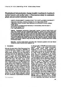
electromagnetic field and high SERS activity. The semiconductor material TiO2 with a wide band 2 of 11 gap is usually selected in many important applications areas, such as catalytic [17–20] and antimicrobial [21–23] applications, due to its merits including low cost, high stability, and bio-compatibility. Most important SERS substrates with Ag andsuch TiOas 2 composite components are prepared by a usually selected in many applications areas, catalytic [17–20] and antimicrobial [21–23] chemical method, such as the including sol-gel method, chemical vapor deposition, and so on. However, in applications, due to its merits low cost, high stability, and bio-compatibility. Most SERS order to obtain a SERS substrate comprising a nanoarray with a large area and high ordered substrates with Ag and TiO2 composite components are prepared by a chemical method, such as structures, a physical preparation with and simple stepsHowever, is a goodinchoice One such the sol-gel method, chemical vaporprocess deposition, so on. order [24,25]. to obtain a SERS simple process is magnetron prepared by magnetron have good substrate comprising a nanoarraysputtering. with a largeFilms area and high ordered structures,sputtering a physical preparation stabilitywith and simple uniformity. Inathis paper, nanostructure arrays consisting of TiO 2 and Ag process steps is good choicedifferent [24,25]. One such simple process is magnetron sputtering. composites are fabricated by the magnetron sputtering system. Inuniformity. comparisonIntothis thepaper, pure Ag array, Films prepared by magnetron sputtering have good stability and different the properties of the nanostructure array for a TiO 2 /Ag bilayer and a TiO 2 -Ag monolayer deposited nanostructure arrays consisting of TiO2 and Ag composites are fabricated by the magnetron sputtering on a two-dimensional array investigated by 4-Amino-thiophenol (PATP) as the probing system. In comparisoncolloidal to the pure Agare array, the properties of the nanostructure array for a TiO 2 /Ag molecule. bilayer and a TiO2 -Ag monolayer deposited on a two-dimensional colloidal array are investigated by 4-Amino-thiophenol (PATP) as the probing molecule. 2. Results and Discussion 2. Results and Discussion 2.1. Preparation and Characterization of the Nano Composite Structure 2.1. Preparation and Characterization of the Nano Composite Structure We prepared the polystyrene (PS) colloidal spheres Arrays with size of 200 nm by the We prepared the polystyrene (PS) colloidal spheresin Arrays withsolution size of 200 nm by the self-assembly self-assembly technique. The Si wafer was immersed a mixed containing NH 4OH, H2O2, technique. Si wafer ratio was immersed in a was mixed solution containing H2were O at 2 O2 , and and H2O atThe a volume of 1:2:6, and heated at 300 °C for NH 5-104 OH, min.HThen, they ◦ C for 5-10 min. Then, they were ultrasonically cleaned aultrasonically volume ratio cleaned of 1:2:6, for and10–15 was heated at 300 min in deionized water and alcohol alternately. This cleaning step for min three in deionized water and alcohol alternately. cleaning step was repeated times. was10–15 repeated times. The Si wafer was soaked in 2%This sodium sulfate solution for 24 hthree to obtain a The Si wafer was soaked in 2% sodium sulfate solution for 24 h to obtain a hydrophilic substrate hydrophilic substrate surface. Alcohol and 200 nm polystyrene were mixed with a volume ratio of surface. Alcohol and nm polystyrene were ratio of 1:1. we 1:1. Subsequently, we200 dropped the mixture on mixed the Si with wafer,a volume which was kept in aSubsequently, sodium dodecyl dropped the mixture on the Si wafer, which was kept in a sodium dodecyl sulfate solution and slowly sulfate solution and slowly immersed into a glass vessel. The PS particles formed unordered immersed a glass vessel. PS particles unorderedexcess monolayer on the water surface. monolayerinto films on the waterThe surface. Finally,formed after absorbing waterfilms by filter paper and being Finally, after absorbing excess water by filter paper and being dried completely in air by static natural dried completely in air by static natural evaporation, two-dimensional polystyrene beads in evaporation, two-dimensional polystyrene beads inon closely-packed arrays formed closely-packed monolayer ordered arrays formed the surface ofmonolayer the silicon ordered substrate. on the surface of the TiO silicon substrate. Semiconductor 2 and metal Ag targets were deposited onto 200-nm PS colloidal spheres in Semiconductor TiO and metaltoAg targets the were deposited ontoof200-nm PS colloidal spheres in the 2 system the magnetron sputtering fabricate nanocap arrays the TiO 2 (10 nm)/Ag (10–40 nm) magnetron sputtering system to fabricate the arrays of theTiO TiO22-Ag (10 nm)/Ag nm) bilayer bilayer with different Ag thicknesses andnanocap the co-sputtered (10 nm)(10–40 monolayer. The with different Ag thicknesses and the co-sputtered TiO -Ag (10 nm) monolayer. The fabrication process 2 fabrication process is given in Figure 1. For comparison, TiO2 and Ag were alternatively sputtered is given in Figure 1.toFor comparison, TiO2monolayer and Ag were alternatively and co-sputtered to and co-sputtered form bilayer and nanocap arrays,sputtered respectively. The TiO2 was form bilayerinand arrays, respectively. TheS1. TiO amorphous in magnetron the bilayer 2 was amorphous themonolayer bilayer andnanocap monolayer, as shown in Figure The simple and facile and monolayer, as shown in Figure S1. The simple and facile magnetron sputtering technology sputtering technology was chosen to fabricate the nanostructure array, which avoids the necessity of was chosen tosteps fabricate thefabrication. nanostructure array, which avoids the necessity of sophisticated steps sophisticated during during fabrication. Nanomaterials 2017, 7, 159
Figure 1. Schematic diagram of the preparation preparation process processfor forthe thenanocap nanocaparrays arraysof ofthe theTiO TiO22/Ag /Ag bilayer and the TiO TiO22-Ag monolayer.
Nanomaterials 2017, 7, 159 Nanomaterials 2017, 7, 159
3 of 11 3 of 11
Figures2a–d 2a–dshow show the the SEM SEM images for the t nm (t =(t 10 nm,nm, 20 nm, 30 Figure the bilayer bilayer TiO TiO22(10 (10nm)/Ag nm)/Ag t nm = 10 20 nm, nm,nm, 40 40 nm) onon thethe PSPS template. The aggregations 30 nm) template. The aggregationsofofparticles particleson onthe thesurface surfaceof ofPS PS became became obvious, obvious, and surface roughness decreased as the Ag thickness increased from 10 nm to 40 nm. The amplified cross-section images show that the thickness of the films increased gradually and the morphologies changed from spherical to columnar shapes. When the PS colloidal colloidal sphere sphere was used used as as the the template, template, spherical substrates substratesinduced inducedthe thefilm filmtotogrow grow the vertical direction sphere surface, the spherical inin the vertical direction on on thethe sphere surface, andand the the adjacent nanocaps connected toother each when other the when very Ag2 and TiO2 adjacent nanocaps werewere connected to each filmthe wasfilm verywas thick. Agthick. and TiO elements elements were distributed on of thethe surface of randomly, the nanocap and the element analysis were distributed on the surface nanocap andrandomly, the element analysis mapping of the mapping of the TiO nm)/Ag (10 nm)-coated surface is shown TiO (102 (10 nm)-coated nanocap surfacenanocap is shown in Figure S2. in Figure S2. 2 (10 nm)/Ag
Figure 2. SEM images of bilayer TiO2 (10 nm)/Ag t nm (from (a) to (d), t = 10 nm, 20 nm, 30 nm, 40 nm) Figure 2. SEM images of bilayer TiO2 (10 nm)/Ag t nm (from (a) to (d), t = 10 nm, 20 nm, 30 nm, 40 nm) on the PS template for different thicknesses of the Ag layer. The illustration is the cross-section of the on the PS template for different thicknesses of the Ag layer. The illustration is the cross-section of sample. the sample.
2.2. SERS Study of PS/TiO2/Ag and PS/Ag 2.2. SERS Study of PS/TiO2 /Ag and PS/Ag Figure 3 shows the SERS spectrum of PATP adsorbed on the PS/TiO2/Ag bilayer from 1 × 10⁻³ Figure 3 shows the SERS spectrum of PATP adsorbed on the PS/TiO2 /Ag bilayer from mol/L aqueous solution. For the substrate PS/TiO2/Ag bilayer and PS/Ag monolayer, the relative 1 × 10⁻³ mol/L aqueous solution. For the substrate PS/TiO2 /Ag bilayer and PS/Ag monolayer, intensity and the position of Raman peaks are significantly different. In the PS/TiO2/Ag spectra the relative intensity and the position of Raman peaks are significantly different. In the PS/TiO2 /Ag (Figure 3a), PATP molecules exhibit characteristic peaks located at 1008, 1072, 1141, 1188, 1302, 1390, spectra (Figure 3a), PATP molecules exhibit characteristic peaks located at 1008, 1072, 1141, 1188, 1440, 1472, and 1577 cm−1. However, PATP molecules on the PS/Ag substrate show the characteristic 1302, 1390, 1440, 1472, and 1577 cm−1 . However, PATP molecules on the PS/Ag substrate show the peaks located at 1008, 1071, 1140, 1182, 1301, 1389, 1439, 1472, and 1577 cm−1 (Figure−13b). Among characteristic peaks located at 1008, 1071, 1140, 1182,−11301, 1389, 1439, 1472, and 1577 cm (Figure 3b). these, the peaks at around 1072, 1188, and 1472 cm are assigned to the υ(C–S), δ(C–H), and υ(C–C) Among these, the peaks at around 1072, 1188, and 1472 cm−1 are assigned to the υ(C–S), δ(C–H), stretching vibrations, respectively, which are dominated by characteristic a1 vibrational modes and υ(C–C) stretching vibrations, respectively, which are dominated by characteristic a1 vibrational [26–28]. The δ(C–H) at 1140 cm−1, [υ(C–C) + δ(C–H)] at 1390 and 1440 cm−1, and υ(C–C) at 1577 cm−1 − 1 − 1 modes [26–28]. The δ(C–H) at 1140 cm , [υ(C–C) + δ(C–H)] at 1390 and 1440 cm , and υ(C–C) at are interpreted as b2 modes [29–31] (Table 1). 1577 cm−1 are interpreted as b2 modes [29–31] (Table 1). Table 1. Wavenumbers and assignments of bands in the SERS spectrum of PATP molecule.
Wavenumber (cm−1) PS/TiO2/Ag 1577m 1472w 1440υs
PS/Ag 1577m 1472w 1439υs
Band Assignment υCC, 8b(b2) υCC, 19a(a1) υCC + δCH, 19b(b2)
1188w 1141υs 1072m 1008w
1182w 1140υs 1071m 1008w
δCH, 9a(a1) δCH, 9b(b2) υCS, 7a(a1) γCC + γCCC, 18a(a1)
Approximate description of the modes (υ, stretch; δ and γ, bend). Frequencies (in cm−1) followed by 4 of 11 relative intensities (υs, very strong; s, strong; m, medium; w, weak).
Nanomaterials 2017, 7, 159
Figure 3. SERS spectra of (a)of PS/TiO /Ag nm) bilayer; (b) PS/Ag monolayer Figure 3. SERS spectra (a) PS/TiO 2 (10 nm)(10–40 /Ag (10–40 nm) bilayer; (b)(10–40 PS/Agnm) (10–40 nm) 2 (10 nm) resembled on resembled 200 nm PSon template; absorption of PS/TiO nm)/Ag (10–40 nm) monolayer 200 nm (c) PS UV-Vis template; (c) UV-Visspectra absorption spectra2 (10 of PS/TiO 2 (10 nm)/Ag bilayer; (d) UV-Vis absorption spectra of PS/Ag (10–40 nm).(10–40 nm). (10–40 nm) bilayer; (d) UV-Vis absorption spectra of PS/Ag
InTable the UV-Vis spectra of TiO2/Ag bilayer 3c), spectrum two major absorption bands are 1. Wavenumbers andthe assignments of bands(Figure in the SERS of PATP molecule. observed. The band around 200–400 nm corresponds to the band gap absorption of TiO2-Ag, while the varying around 400–800 nm is attributed Wavenumber (cm−1 ) to the surface plasmon resonance (SPR) absorption of Band Assignment Ag. The blue shift of absorption peaks and the decrease of resonance intensity can be observed when PS/TiO PS/Ag 2 /Ag the Ag thickness increases from 10 nm to 40 nm, which can be ascribed to the reconstruction of a new 1577m 1577m υCC, 8b(b ) Fermi level in TiO2-Ag bilayer due to the special optical properties of TiO22 that can provide a large 1472w 1472w υCC, 19a(a1 ) number of electrons 1440υs [32]. The peak changes in the TiO2/AgυCC bilayer should 1439υs + δCH, 19b(b2be ) derived from the interaction between the chemical absorption of the PATP molecule and 3(b the2 )nanostructure of the 1390s 1389s δCH + υCC, 1302w the charge transfer 1301w(CT) is calculated υCC for + δCH, ) TiO2/Ag bilayer. Therefore, the 14(b TiO22/Ag bilayer and pure 1182win Figure 4. FigureδCH, 9a(a1 ) the UV-Vis spectra of Ag monolayer arrays,1188w and the results are shown 3d presents 1140υs δCH, 9b(b 2 ) The broad absorption the as-prepared pure 1141υs Ag nanomaterials with four different thicknesses of Ag. 1072m 1071m υCS, 7a(a1 ) covering the range of 400–800 nm should be ascribed to the SPR of Ag. The red shift phenomenon 1008w 1008w γCC + γCCC, 18a(a1 ) appears when the thickness of Ag increases. The wavelength of the SPR −band is related to the Approximate description of the modes (υ, stretch; δ and γ, bend). Frequencies (in cm 1 ) followed by relative particle size, shape, and surrounding environment [33,34]. In addition, the spectra of Ag 40 nm show intensities (υs, very strong; s, strong; m, medium; w, weak). a sharp rise at about 320 nm, which corresponds to the onset of the interband absorption threshold energy hv = 3.9 eV of Ag [32]. In contrast to the Ag monolayer, the characteristic peaks exhibited are In the UV-Vis spectra of the TiO2 /Ag bilayer (Figure 3c), two major absorption bands are observed. partly in the blue shift in the TiO2/Ag bilayer. For the TiO2/Ag bilayer, the SERS intensities decreased The band around 200–400 nm corresponds to the band gap absorption of TiO2 -Ag, while the varying with the increase of Ag thickness, and the maximum value is observed when the thickness of the around 400–800 is attributed to the shows surface absorption The sublayer Ag is nm 10 nm, while the sample theplasmon weakest resonance signal when(SPR) the sublayer of AgofisAg. 40 nm. blue shift of absorption peaks and the decrease of resonance intensity can be observed when the However, for the Ag monolayer array, the intensity of the SERS signals increases with theincrease ofAg thickness increases from 10 nm to 40 nm, which can be ascribed to the reconstruction of a new Fermi level in TiO2 -Ag bilayer due to the special optical properties of TiO2 that can provide a large number of electrons [32]. The peak changes in the TiO2 /Ag bilayer should be derived from the interaction between the chemical absorption of the PATP molecule and the nanostructure of the TiO2 /Ag bilayer. Therefore, the charge transfer (CT) is calculated for the TiO2 /Ag bilayer and pure Ag monolayer arrays, and the results are shown in Figure 4. Figure 3d presents the UV-Vis spectra of the as-prepared pure Ag nanomaterials with four different thicknesses of Ag. The broad absorption covering the range of 400–800 nm should be ascribed to the SPR of Ag. The red shift phenomenon appears when the thickness of Ag increases. The wavelength of the SPR band is related to the particle size, shape, and surrounding environment [33,34]. In addition, the spectra of Ag 40 nm show a sharp rise at about
Nanomaterials 2017, 7, 159
5 of 11
320 nm, which corresponds to the onset of the interband absorption threshold energy hv = 3.9 eV of Ag [32]. In contrast to the Ag monolayer, the characteristic peaks exhibited are partly in the blue shift in the TiO2 /Ag bilayer. For the TiO2 /Ag bilayer, the SERS intensities decreased with the increase of Ag thickness, and the maximum value is observed when the thickness of the sublayer Ag is 105 of nm, Nanomaterials 2017, 7, 159 11 while the sample shows the weakest signal when the sublayer of Ag is 40 nm. However, for the Ag monolayer array, the of the SERS increases theincrease Ag thickness, and the Ag thickness, andintensity the maximum valuesignals is observed for with an Ag thickness of of the 40 nm. Furthermore, the maximum value observed thickness nm. Furthermore, the increase of the with the increase of isthe contentfor of an Ag,Agthe 1188 cmof−1 40 characteristic peaks with of PATP molecules on − 1 −1 −1 content Ag, the 1188 cm thecharacteristic peaks of PATP molecules bilayer TiO 2/Agof bilayer exhibited blue shift from 1188 cm of TiO2/Ag on (10TiO nm) to 1182 cmexhibited for the 2 /Ag 1 for the3b), the blueTiO shift from cm−1 of4a). TiOFor nm) 1182 cm−(Figure sample TiO2 /Ag (40show nm) sample 2/Ag (40 1188 nm) (Figure the(10 pure Agtomonolayer the peaks do not 2 /Ag any shift. The above results that (Figure TiO2 plays in theany peak shiftsThe of above PATP (Figure 4a). For the pure Agindicate monolayer 3b), an theimportant peaks do role not show shift. results indicate that TiO an important role in peak shiftsAg of PATP absorbed on the molecules absorbed on the TiO 2/Ag bilayer. AstheTiO 2 and form molecules composites, the size of 2 plays TiO2 /Ag bilayer. As TiOThe and Ag form composites, the size of nanoparticles changes. The peak shifts nanoparticles changes. peak shifts for TiO 2 /Ag can be reduced when the thickness of the Ag 2 layer increases. for TiO 2 /Ag can be reduced when the thickness of the Ag layer increases.
Figure 4. Column statistics of of relative relative peak peak intensity intensity and andcharge chargetransfer transferfor for(a)(a)I1391 I1391/I/I1072 1072 of Figure 4. Column statistics of the the PS/TiO 2 (10 nm)/Ag (10–40 nm) bilayer and (b) I 1389 /I 1071 of the pure PS/Ag (10–40 nm) monolayer. PS/TiO2 (10 nm)/Ag (10–40 nm) bilayer and (b) I1389 /I1071 of the pure PS/Ag (10–40 nm) monolayer.
The band at the 1072 cm−1−(a 1) peak of the C–S stretching vibration and the band at about 1391 The band at the 1072 cm 1 (a1 ) peak of the C–S stretching vibration and the band at about cm (b2) of the C–H and C–C bending vibrations are used to calculate the charge transfer degree. It is 1391 cm−1 (b2 ) of the C–H and C–C bending vibrations are used to calculate −1the charge transfer degree. clear that the ratio of relative intensities of the two Raman peaks (1391 cm and 1072 cm−1) of PATP − 1 It is clear that the ratio of relative intensities of the two Raman peaks (1391 cm and 1072 cm−1 ) molecules adsorbed on TiO2/Ag bilayer is remarkably changed. The charge transfer of the bilayer of PATP molecules adsorbed on TiO2 /Ag bilayer is remarkably changed. The charge transfer of the decreases upon increasing the thickness of the Ag layer, which indicates that the TiO2 on the surface bilayer decreases upon increasing the thickness of the Ag layer, which indicates that the TiO2 on of the bilayer plays an important role in charge transfer. We believe that the mixture components the surface of the bilayer plays an important role in charge transfer. We believe that the mixture consisting of Ag and TiO2 occur at the surface of the bilayer due to the interface diffusion between components consisting of Ag and TiO2 occur at the surface of the bilayer due to the interface diffusion the TiO2 and Ag sublayer when a thinner Ag film is deposited on TiO2. Furthermore, TiO2 can between the TiO2 and Ag sublayer when a thinner Ag film is deposited on TiO2 . Furthermore, TiO2 provide a large number of electrons due to its unique photoelectric properties and generate a new can provide a large number of electrons due to its unique photoelectric properties and generate a new Fermi level in the composite structure, which causes a change in the charge transfer degree between Fermi level in the composite structure, which causes a change in the charge transfer degree between the composites and PATP molecules. In general, the changes in the relative Raman band intensities the composites and PATP molecules. In general, the changes in the relative Raman band intensities between different vibrational modes are closely related to the chemical mechanism of SERS [35]. between different vibrational modes are closely related to the chemical mechanism of SERS [35]. We use the concept of the “degree of CT ( CT )”, proposed by Lombardi et al. [36,37] to We use the concept of the “degree of CT (ρCT)”, proposed by Lombardi et al. [36,37] to estimate estimate the influence of the contribution of CT resonance the SERS intensity quantitatively. the influence of the contribution of CT resonance to the SERStointensity quantitatively. The ρCT (k) The can CT (k ) can bebydetermined by following equation: be determined following equation: −1
II kk ((CT CT))− IIkk((SPR SPR) ) ρCT CT(k) kk (k) = 0 0 II (CT CT))+ II ((SPR SPR) )
(1) (1)
Here, kk isisan used to identify individual molecular lines lines in theinRaman spectrum. We choose anindex index used to identify individual molecular the Raman spectrum. We − 1 − 1 −1 −1 the intensities of two peaks (1072 cm (1072 and 1391 a spectral region for better understanding. choose the intensities of two peaks cm cmand) in 1391 cm ) in a spectral region for better The 1072 cm−1 (a totally symmetric to the SERS signal contributions from SPR, whosefrom intensity understanding. The cm−1 (a1) is totally symmetric to the SERS signal contributions SPR, 1 ) is1072 0 ( SPR ), and for this k ( SPR ) = I 0 ( SPR ).k The other0peak, 1391 cm−1 (b ), is 0 is denoted as I line I 2 whose intensity is denoted as I ( SPR ) , and for this line I ( SPR ) I ( SPR ) . The other peak, non-totally symmetric (intensity denoted as I k (CT )). It is the measured intensity in the region of the k 1391 cm−1 (b2), is non-totally symmetric (intensity denoted as I (CT ) ). It is the measured intensity
in the region of the spectrum where CT resonance makes an additional contribution to the SERS intensity, excluding the contribution of SPR [31]. In this case,
I k (SPR ) is normally small or equal
to zero. Then, Equation (2) can be approximately expressed as follows:
Nanomaterials 2017, 7, 159
6 of 11
spectrum where CT resonance makes an additional contribution to the SERS intensity, excluding the contribution of SPR [31]. In this case, I k (SPR) is normally small or equal to zero. Then, Equation (2) Nanomaterials 2017, 7, 159 6 of 11 can be approximately expressed as follows:
bba212 (2) a b2 CT 1 +1 a1 (2) b 1 2 In Figure 4a, the change of relative peak intensities aof 1 I1391 /I1072 vibrational mode bands indicates ρCT =
the CT transition from the Fermi level of the TiO2 -Ag composites to the lowest unoccupied molecular In Figure 4a, the change of relative peak intensities of I1391/I1072 vibrational mode bands indicates orbitals (LUMO) of the PATP molecules. With an increasing concentration of Ag, the charges of the the CT transition from the Fermi level of the TiO2-Ag composites to the lowest unoccupied TiO2 -Ag-PATP complex can beofredistributed further, resulting in a moreconcentration suitable CT of state molecular orbitals (LUMO) the PATP molecules. With an increasing Ag,involved the in thecharges SERS-CT process. The degree of CT (ρCT) shows the match degree of excitation energy of the TiO2-Ag-PATP complex can be redistributed further, resulting in a more suitable CT and the energy difference between the process. Fermi level of the TiO the LUMO 2 -Ag CT ) shows and state involved in the SERS-CT The degree of CT ( composites the match degreeofofPATP, indicating that the b mode of PATP is selectively enhanced via the CT resonance transition. 2 excitation energy and the energy difference between the Fermi level of the TiO2-Ag compositesHowever, and in thethe pure Ag monolayer (Figure 4b), provides number of electrons in the via charge transfer LUMO of PATP, indicating thatAgthe b2 modea large of PATP is selectively enhanced the CT process so thattransition. more freeHowever, electronsincan provided, which (Figure makes 4b), the charge transfer degree increase resonance thebe pure Ag monolayer Ag provides a large number charge transfer process so that more free electrons can be provided, which makes with of theelectrons increaseininthe Ag content. the charge transfer degree increase with the increase in Ag content.
2.3. Enhancement Factor (EF) of PS/TiO2 /Ag and PS/TiO2 :Ag 2.3. Enhancement Factor (EF) of PS/TiO2/Ag and PS/TiO2:Ag
Except for the charge transfer, the change of the surface morphology of nanocaps array is another transfer, the change of the surface morphology of nanocaps array is importantExcept factorfor forthe thecharge enhancement of SERS for PS/TiO2 (10 nm)/Ag (10 nm) bilayer. As the SEM another important factor for the enhancement of SERS for PS/TiO2 (10 nm)/Ag (10 nm) bilayer. As image of Figure 2 shows, a 10-nm Ag film was deposited on TiO2 , and the composite of Ag and TiO2 the SEM image of Figure 2 shows, a 10-nm Ag film was deposited on TiO2, and the composite of Ag increased the surface roughness, leading to the enhancement of the SERS signal. When the TiO2 and TiO2 increased the surface roughness, leading to the enhancement of the SERS signal. When the layerTiO was covered completely by the Ag film, the SERS signals decreased with the increase of the Ag 2 layer was covered completely by the Ag film, the SERS signals decreased with the increase of thickness. investigate the effect the of the surface and composite consisting of TiO Ag the AgTo thickness. To investigate effect of the roughness surface roughness and composite consisting of TiO 2 2 and on SERS, theon co-sputtered TiO2 -Ag (20TiO nm) monolayer was deposited on a PS template. Figure 5a–d and Ag SERS, the co-sputtered 2-Ag (20 nm) monolayer was deposited on a PS template. 5a–dimages show the images andofSERS spectra the TiO2-Ag monolayer different showFigure the SEM andSEM SERS spectra the TiO monolayer with differentwith contents of TiO2 . 2 -Agof contents of TiO 2 . When the Ti content increased from 10 at.% to 28 at.%, the particles sizes and the When the Ti content increased from 10 at.% to 28 at.%, the particles sizes and the surface roughness surfaceThe roughness increased. The SERS increased firstAlso, and the thenmaximum decreased.occurred Also, thewhen increased. SERS intensity increased firstintensity and then decreased. maximum occurred when the TiO2 atomic percent content was 15%, as it was confirmed that the the TiO2 atomic percent content was 15%, as it was confirmed that the optimum surface roughness optimum surface roughness provided abundant hot spots that were created by the composite of TiO2 provided abundant hot spots that were created by the composite of TiO2 and Ag. Compared to the and Ag. Compared to the bilayer samples, TEM images show the small Ag particles formed in the bilayer samples, monolayer TEM images show small Ag particles formed the co-sputtered monolayer co-sputtered (Figure 6). the In addition, HRTEM images show in that TiO 2 is amorphous and (Figure addition, HRTEM images show thatabout TiO28isnm, amorphous and the Agthat particles trapped in the6). AgIn particles trapped in amorphous TiO2 are which is smaller than of the bilayer amorphous TiO aboutthat 8 nm, which is smaller that ofinhibit the bilayer of 30 nm,and which shows of 30 nm, which co-sputtered TiO2 canthan effectively the aggregation growth of that 2 areshows co-sputtered TiO2 can effectively inhibit the aggregation and growth of Ag nanoparticles. Ag nanoparticles.
Figure 5. (a–c) images andSERS (d) SERS spectra of TiO 2-Ag (20 nm) with different TiO2 atomic Figure 5. (a–c) SEMSEM images and (d) spectra of TiO 2 -Ag (20 nm) with different TiO2 atomic percent percent contents: (a) 10%; (b) 15%; (c) 25%. contents: (a) 10%; (b) 15%; (c) 25%.
Nanomaterials 2017, 7, 159
Nanomaterials 2017, 7, 159 Nanomaterials 2017, 7, 159
7 of 11
7 of 11 7 of 11
Figure 6. TEM and HRTEM images of (a,c) the TiO2 (10 nm)/Ag (10 nm) bilayer, and (b,d) the co-sputtered TiO2-Ag (20 nm) monolayer. Figure 6. enhancement TEM and HRTEM images of (a,c) the TiO2 (10 nm)/Ag (10 nm)selected bilayer, and (b,d) The SERS factor (EF)of is(a,c) calculated 10 randomly forthe the Figure 6. TEM and HRTEM images the TiO2from (10 nm)/Ag (10 nm) bilayer,points and (b,d) the TiO2 co-sputtered TiO 2-Ag (20and nm) TiO monolayer. (10 nm)/Ag (10 nm) bilayer 2-Ag (20 nm) co-sputtered monolayer according to the equation co-sputtered TiO2 -Ag (20 nm) monolayer. [38–40] (Figure 7), EF ( I SERS Nbulk ) /( Ibulk Nads) , where I SERS and I bulk are the SERS The SERS enhancement factor (EF) is calculated from 10 randomly selected points for the TiO2 −1 assigned to PATP absorbed on TiO2/Ag arrays and the Raman intensity of the bands at 1440 cmTiO SERS enhancement factor (EF) is(20 calculated from 10 randomly points the TiO2 (10The nm)/Ag (10 nm) bilayer and 2-Ag nm) co-sputtered monolayerselected according to thefor equation −1 (10 nm)/Ag (10 bilayer and -Ag (20 nm) co-sputtered monolayer according equation [38–40] N tobulkthe are cRSVN intensity of(Figure thenm) band atEF 1403 to the solid PATP, respectively. is the 2assigned (cm ITiO [38–40] 7), the ASERS SERS Nbulk ) /( I bulk N ads ) , where I SERS and Ibulk (Figure 7), EF = ( I × N ) / ( I × N ) , where I and I are the SERS intensity of the bands SERS bulk ads tovolume bulk −1 scattering average number molecules the (V) for the (non-SERS) intensity of theof bands at bulk 1440incm assigned PATPSERS absorbed onRaman TiO2/Ag arrays andmeasurement. the Raman −1 assigned to PATP absorbed on TiO /Ag arrays and the Raman intensity of the band at at 1440 cm 2 N adsis is The molar of concentration (cRS)cmof−1 assigned the PATPtoanalyte on the reference region is 1 mM. N cRSVN intensity the band at 1403 the solid PATP, respectively. thethe bulk 1403 cm−1 assigned to the solid PATP, respectively. Nbulk = cRSVNA is the average number of Amolecules average adsorbedinmolecules in volume the scattering volume the SERS experiments. averagenumber number of molecules the scattering (V) for the Ramanfor (non-SERS) measurement. in the scattering volume (V) for the Raman (non-SERS) measurement. The molar concentration (cRS) of concentration (cRS)Nof PATP analyte on theaverage reference region 1 mM. is the NThe molar Nanalyte Aon , reference where is the of PS with a diameter of N 200 and ads nm, d the ads d Alaser N /the the PATP region is 1number mM. Nadsdensity is the number ofisadsorbed molecules in average the scattering volume for the SERS experiments. the scattering volume foradsorbed the SERS experiments. N = N A A /δ, where N is the number density Alaser A is thenumber area of of the focal lasermolecules spot. The in laser spot is a circle with a diameter of 1 μm. is the ads d laser N d N Nsurface N Alaserof ANone /of 200 ,PS where the number density PS diameter of 200 nm, of PS with a ddiameter nm, is the areanm, of the focal spot.a The laser spot is aby circle with d Ais ads laser half area withand aNdiameter of 200 and δofislaser thewith surface area occupied a and single aPATP diameter µm. Athe issubstrate the half surface area of one PSiswith a to diameter ofnm 2002 [41]. nm, δthe isAthe surface N Alaseradsorbed is of the1 area the focal laser spot. The laser a circle with a diameter of and 1For μm. is the onof value, which isspot estimated be 0.20 NRenishaw 2 [41]. area occupied by a single PATP adsorbed on the substrate value, which is estimated to be 0.20 nm half surface area of one PS with with 633-nm a diameter of excitation, 200 nm, andthe δ is the surface area depth occupied byμm. a single Nbulk Micro-Raman spectrometer laser effective focused is 19 ForPATP the Renishaw Micro-Raman spectrometer with 633-nm laser excitation, the effective focused depth 2 on the substrate value, which is estimated to be 0.20 nm [41]. For the Renishaw is 16 and 9.62 × 10⁷, respectively. I NNadsadsorbed and can beNcalculated to be 1.77to×be 101.77 are 261.3 and SERS /IISERS bulk /I 19 µm. and can be calculated × 1016 andthe 9.62 × 10⁷ , respectively. 261.3 bulk ads bulk are Nbulk Micro-Raman spectrometer with 633-nm laser excitation, effective focused depth is 19 μm. 17.2317.23 for for the the TiOTiO 2/Ag bilayer andand thethe TiO 2-Ag co-sputtered 1391cm cm−−11, and bilayer TiO co-sputteredmonolayer monolayeratatthe the band of 1391 2 /Ag 2 -Ag 16 and 9.62 × 10⁷, respectively. I N / I and can be calculated to be 1.77 × 10 are 261.3 and 10 and 3.17 × SERS bulk ads Therefore, respectively. Therefore,EFEF is calculated be× 4.81 109 the for the 2TiO bilayer respectively. is calculated to be to 4.81 1010× 10 and 3.17 × 10⁹ for TiO /Ag2/Ag bilayer andand the −1, 17.23 for the TiO 2 /Ag bilayer and the TiO 2 -Ag co-sputtered monolayer at the band of 1391prepared cm the 2TiO co-sputtered monolayer, respectively. showthe that the monolayer TiO -Ag2-Ag co-sputtered monolayer, respectively. TheseThese resultsresults show that monolayer prepared by the 10 and 3.17 × 10⁹ for the TiO2/Ag bilayer and EFhas Therefore, is calculated toand be 4.81 ×and 10 byrespectively. the co-sputtering method better homogeneity SERS property those of the bilayer. co-sputtering method has better homogeneity SERS property than thosethan of the bilayer. the TiO2-Ag co-sputtered monolayer, respectively. These results show that the monolayer prepared by the co-sputtering method has better homogeneity and SERS property than those of the bilayer.
Figure 7. 7. Reproducibility Reproducibility test test for forSERS SERSspectra spectraof ofthe theTiO TiO22 (10 (10 nm)/Ag nm)/Ag (10 nm) bilayer. Figure Figure 7. Reproducibility test for SERS spectra of the TiO2 (10 nm)/Ag (10 nm) bilayer.
Nanomaterials 2017, 7, 159
8 of 11
3. Materials and Methods 4-Aminothiophenol (PATP) with a purity of 99.9% was used as the probing molecule. Sodium dodecyl sulfate and ethanol were purchased from Sigma Aldrich (St. Louis, MO, USA). Concentration of 10 wt % of (particle deviation less than 10%) monodisperse polystyrene (PS) colloidal spheres with a size of 200 nm were purchased from The Duke (Durham, NC, USA). The Ag and TiO2 targets with a purity of 99.99% (wt %) used in the experiment were purchased from Beijing TIANRY Science & Technology Developing Center (Beijing, China). Silicon wafer was purchased from Hefei Kejing Materials Technology Co., Ltd (Hefei, China). Ultrapure water (18.0 MΩ·cm−1 ) was used throughout the present study. The film deposition was performed in a magnetron sputtering system with JGP-560C. During deposition, the base vacuum degree was 2 × 10⁻⁴ Pa, and the argon pressure was 0.6 Pa. The sputtering powers of TiO2 were 50 W, 100 W, and 150 W; the sputtering power of Ag was 5.4 W. The PS (200 nm) monolayer colloidal array was prepared by using the self-assembly method [42]. The samples were immersed in PATP solution with a concentration of 3% for more than 30 min to reach saturation adsorption. The morphology and microstructure of the samples were investigated by field emission scanning electron microscopy (SEM) and electron microscopy (TEM). The SEM images were characterized under an accelerating voltage of 5.0 KV (model JSM-7800F, JEOL, Tokyo, Japan). TEM images were recorded on JEM-2100HR (JEOL, Tokyo, Japan). UV-Vis spectra were measured on a Shimadzu UV-3600 spectrophotometer (Shimadzu, Kyoto, Japan). Raman spectra were obtained with a Renishaw Raman system model 2000 confocal microscopy spectrometer (Renishaw, London, UK). An air-cooled argon ion laser (Renishaw, London, UK) with 633-nm radiation from (40 mW, power out of 0.1%) was used for the SERS. The spectra were recorded with an accumulation time of 10 s. Film thickness was measured by a Stylus Profiler (Vecco Dektak 150, VEECO, Plainview, NY, USA). 4. Conclusions In summary, we fabricated SERS substrate of TiO2 and Ag metal-semiconductor composite onto a 200-nm PS template by using a combination of the self-assembly technique and the magnetron sputtering method. Compared with the pure Ag film, the TiO2 /Ag bilayer showed significant SERS enhancement when the Ag thickness was thin, which was ascribed to the electromagnetic mechanism (EM) and charge-transfer (CT) enhancement mechanisms in the metal-semiconductor system. The optimized TiO2 contents at the surface of the nanostructure not only improved the enhancement of SERS but also effectively inhibited the aggregation and growth of Ag nanoparticles, which was confirmed by the co-sputtered TiO2 -Ag monolayer. The TiO2 -Ag nanocaps array exhibited a good periodicity and uniformity; the enhancement factor reached 4.81 × 10¹⁰ for the TiO2 /Ag bilayer and 3.17 × 10⁹ for the TiO2 -Ag monolayer, respectively. Supplementary Materials: The following are available online at http://www.mdpi.com/2079-4991/7/7/159/s1, Figure S1: XRD patterns of samples for TiO2 /Ag bilayer and monolayer TiO2 deposited on PS200 nm templates; Figure S2: The element analysis mapping of bilayer TiO2 (10 nm)/Ag (10 nm) nanocap arrays by SEM; Figure S3: SEM of PS200 nm template. Acknowledgments: This work is supported by the National Natural Science Foundation of China (Nos. 61575080, 61675090 and 21676115), National Youth Program Foundation of China (Nos. 21546013, 61405072 and 51609100), Program for the development of Science and Technology of Jilin province (Nos. 20150519024JH, 20150520015JH, 20160101287JC and 20140519003JH), and Technology of Education Department of Jilin Province (Nos. 2016-217 and JJKH20170374KJ). Thank Fan Zhang, Shuang Guo, Renxian Gao and Yang Liu for their contributions to the research and discussion process. Author Contributions: Yaxin Wang and Yongjun Zhang conceived and designed the experiments; Chao Yan performed the experiments and document retrieval; Yaxin Wang and Chao Yan analyzed the data; Yaxin Wang wrote the paper; Lei Chen and Yongjun Zhang contributed significantly to analysis and manuscript preparation; Jinghai Yang helped perform the analysis with constructive theoretical discussions. Conflicts of Interest: The authors declare no conflict of interest.
Nanomaterials 2017, 7, 159
9 of 11
References 1. 2.
3. 4.
5. 6.
7. 8.
9.
10.
11.
12.
13. 14.
15.
16. 17. 18. 19. 20.
Fleischmann, M.; Hendra, P.J.; Mcquillan, A.J. Raman Spectra of Pyridine Adsorbed at a Silver Electrode. Chem. Phys. Lett. 1974, 26, 163–166. [CrossRef] Jeanmaire, D.L.; Duyne, R.P.V. Surface Raman SpectroElectrochemistry Part I. Heterocyclic, Aromatic and Aliphatic Amines Adsorbed on the Anodized Silver Electrode. J. Electroanal. Chem. Interfac. Electrochem. 1997, 84, 1–20. [CrossRef] Ngo, H.T.; Wang, H.N.; Fales, A.M.; Vo-Dinh, T. Label-Free DNA Biosensor Based on SERS Molecular Sentinel on Nanowave Chip. Anal. Chem. 2013, 85, 6378–6383. [CrossRef] [PubMed] Wu, L.; Wang, Z.Y.; Zong, S.F.; Cui, Y.P. Rapid and Reproducible Analysis of Thiocyanate in Real Human Serum and Saliva Using a Droplet SERS-Microfluidic Chip. Biosens. Bioelectron. 2014, 62, 13–18. [CrossRef] [PubMed] Ma, W.; Sun, M.Z.; Xu, L.G.; Wang, L.B.; Kuang, H.; Xu, C.L. A SERS Active Gold Nanostar Dimer for Mercury Ion Detection. Chem. Commun. 2013, 49, 4989–4991. [CrossRef] [PubMed] Shanmukh, S.; Jones, L.; Driskell, J.; Zhao, Y.P.; Dluhy, R.; Tripp, R.A. Rapid and Sensitive Detection of Respiratory Virus Molecular Signatures Using a Silver Nanorod Array SERS Substrate. Nano Lett. 2006, 6, 2630–2636. [CrossRef] [PubMed] Albrecht, M.G.; Creighton, J.A. Anomalously Intense Raman Spectra of Pyridine at a Silver Electrode. J. Am. Chem. Soc. 1997, 99, 5215–5217. [CrossRef] He, S.J.; Liu, K.-K.; Su, S.; Yan, J.; Mao, X.H.; Wang, D.F.; He, Y.; Li, L.-J.; Song, S.P.; Fan, C.H. Graphene-Based High-Efficiency Surface-Enhanced Raman Scattering-Active Platform for Sensitive and Multiplex DNA Detection. Anal. Chem. 2012, 84, 4622–4627. [CrossRef] [PubMed] Bantz, K.C.; Meyer, A.F.; Wittenberg, N.J.; Im, H.; Kurtulus, Ö.; Lee, S.H.; Lindquist, N.C.; Oh, S.-H.; Haynes, C.L. Recent progress in SERS biosensing. Phys. Chem. Chem. Phys. 2011, 13, 11551–11567. [CrossRef] [PubMed] Jiang, Y.X.; Li, J.F.; Wu, D.Y.; Yang, Z.L.; Ren, B.; Hu, J.W.; Chow, Y.L.; Tian, Z.Q. Characterization of surface water on Au core Pt-group metal shell nanoparticles coated electrodes by surface-enhanced Raman spectroscopy. Chem. Commun. 2007, 44, 4608–4610. [CrossRef] [PubMed] Yang, L.B.; Jiang, X.; Ruan, W.D.; Zhao, B.; Xu, W.Q.; Lombard, J.R. Observation of Enhanced Raman Scattering for Molecules Adsorbed on TiO2 nanoparticles: Charge-Transfer Contribution. J. Phys. Chem. C 2008, 112, 20095–20098. [CrossRef] Wang, Y.X.; Song, W.; Ruan, W.D.; Yang, J.X.; Zhao, B.; Lombard, J.R. SERS Spectroscopy to Study an Adsorbate on Nanoscale Thin Film of CuO coated with Ag. J. Phys. Chem. C 2009, 113, 8065–8069. [CrossRef] Xu, W.G.; Mao, N.N.; Zhang, J. Graphene: A Plat form for Surface-Enhanced Raman Spectroscopy. Small 2013, 9, 1206–1224. [CrossRef] [PubMed] Yang, L.B.; Jiang, X.; Ruan, W.D.; Yang, J.X.; Zhao, B.; Xu, W.Q.; Lombardi, J.R. Charge-Transfer-Induced Surface-Enhanced Raman Scattering on Ag–TiO2 Nanocomposites. J. Phys. Chem. C 2009, 113, 16226–16231. [CrossRef] Su, Y.; He, Q.; Yan, X.H.; Fei, J.B.; Cui, Y.; Li, J.B. Peptide Mesocrystals as Templates to Create an Au Surface with Stronger Surface-Enhanced Raman Spectroscopic Properties. Chem. A Eur. J. 2011, 17, 3370–3375. [CrossRef] [PubMed] Bai, J.; Zhou, B.X. Titanium Dioxide Nanomaterials for Sensor Applications. Chem. Rev. 2014, 114, 10131–10176. [CrossRef] [PubMed] Ghicov, A.; Schmuki, P. Self-ordering electrochemistry: A review on growth and functionality of TiO2 nanotubes and other self-aligned MOx structures. Chem. Commun. 2009, 20, 2791–2808. [CrossRef] [PubMed] Fattakhova-Rohlfing, D.; Zaleska, A.; Bein, T. Three-Dimensional Titanium Dioxide Nanomaterials. Chem. Rev. 2014, 114, 9487–9558. [CrossRef] [PubMed] Song, W.; Wang, Y.X.; Zhao, B. Surface-Enhanced Raman Scattering of 4-Mercaptopyridine on the Surface of TiO2 Nanofibers Coated with Ag Nanoparticles. J. Phys. Chem. C 2007, 111, 12786–12791. [CrossRef] Shaviv, E.; Schubert, O.; Alves-Santos, M.; Goldoni, G.; Felice, R.D.; Fatti, F.; Fatti, N.D.; Banin, U.; Sönnichsen, C. Absorption Properties of Metal–Semiconductor Hybrid, Nanoparticles. ACS Nano 2011, 5, 4712–4719. [CrossRef] [PubMed]
Nanomaterials 2017, 7, 159
21.
22.
23.
24. 25.
26.
27.
28. 29.
30.
31.
32.
33.
34.
35. 36. 37. 38.
39.
10 of 11
Venkatasubramanian, R.; Srivastava, R.S.; Misra, R.D.K. Comparative study of antimicrobial and photocatalytic activity in titaniaencapsulated composite nanoparticles with different dopants. Mater. Sci. Technol. 2008, 24, 589–595. [CrossRef] Rawat, J.; Rana, S.; Srivastava, R.S.; Misra, R.D.K. Anti-microbial activity of composite nanoparticles consisting of titania photocatalytic shell and nickel ferrite magnetic core. Mater. Sci. Eng. C 2007, 27, 540–545. [CrossRef] Rana, S.; Rawat, J.; Misra, R.D.K. Anti-microbial active composite nanoparticles with magnetic core and photocatalytic shell: TiO2 –NiFe2 O4 bio-material system. Acta Biomater. 2005, 1, 691–703. [CrossRef] [PubMed] Zhao, J.H.; Lin, J.; Li, X.H.; Zhao, G.N.; Zhang, W.J. Silver nanoparticles deposited inverse opal film as a highly active and uniform SERS substrate. Appl. Surf. Sci. 2015, 347, 514–519. [CrossRef] Klaysri, R.; Praserthdam, P.; Kelly, P.J.; Ratova, M. Deposition of Visible Light-Active C-Doped Titania Films via Magnetron Sputtering Using CO2 as a Source of Carbon. Nanomaterials 2017, 7, 113–128. [CrossRef] [PubMed] Fromm, D.P.; Sundaramurthy, A.; Kinkhabwala, A.; Schuck, P.J.; Kino, G.S.; Moerner, W.E. Exploring the Chemical Enhancement for Surface-Enhanced Raman Scattering with Au Bowtie Nanoantennas. J. Chem. Phys. 2006, 124, 061101. [CrossRef] [PubMed] Hou, X.M.; Zhang, X.L.; Chen, S.T.; Fang, Y.; Yan, J.L.; Li, N.; Qi, P.X. Facile Synthesis of SERS Active Ag Nanoparticles in the Presence of Tri-N-Octylphosphine Sulfide. Appl. Surf. Sci. 2011, 257, 4935–4940. [CrossRef] Dong, B.; Wang, W.; Miller, D.L.; Li, C.Y. Polymer-Single-Crystal@Nanoparticle Nanosandwich for Surface Enhanced Raman Spectroscopy. J. Mater. Chem. 2012, 22, 15526–15529. [CrossRef] Xu, S.C.; Zhang, Y.X.; Luo, Y.Y.; Wang, S.; Ding, H.L.; Xu, J.M.; Li, G.H. Ag-Decorated TiO2 Nanograss for 3D SERS-Active Substrate with Visible Light Self-Cleaning and Reactivation. Analyst 2013, 138, 4519–4525. [CrossRef] [PubMed] Sun, Z.H.; Wang, C.X.; Yang, J.X.; Zhao, B.; Lombard, J.R. Nanoparticle Metal–Semiconductor Charge Transfer in ZnO/PATP/Ag Assemblies by Surface-Enhanced Raman Spectroscopy. J. Phys. Chem. C 2008, 112, 6093–6098. [CrossRef] Wang, Y.; Ji, W.; Sui, H.M.; Kitahama, Y.; Ruan, W.D.; Ozaki, Y.; Zhao, B. Exploring the Effect of Intermolecular H-Bonding: A Study on Charge-Transfer Contribution to Surface-Enhanced Raman Scattering of p-Mercaptobenzoic Acid. J. Phys. Chem. C 2014, 118, 10191–10197. [CrossRef] Yang, L.; Wang, W.H.; Jiang, H.Y.; Zhang, Q.H.; Shan, H.H.; Zhang, M.; Zhu, K.; Lv, J.G.; He, G.; Sun, Z.Q. Improved SERS performance of single-crystalline TiO2 nanosheet arrays with coexposed {001} and {101} facets decorated with Ag nanoparticles. Sens. Actuators B Chem. 2017, 242, 932–939. [CrossRef] Awazu, K.; Fujimaki, M.; Rockstuhl, C.; Tominaga, J.; Murakami, H.; Ohki, Y.; Yoshida, N.; Watanabe, T. A Plasmonic Photocatalyst Consisting of Silver Nanoparticles Embedded in Titanium Dioxide. J. Am. Chem. Soc. 2008, 130, 1676–1680. [CrossRef] [PubMed] Khan, M.M.; Ansari, S.A.; Amal, M.I.; Lee, J.; Cho, M.H. Highly visible light active Ag@TiO2 nanocomposites synthesized using an electrochemically active biofilm: A novel biogenic approach. Nanoscale 2013, 5, 4427–4435. [CrossRef] [PubMed] Han, X.X.; Ji, W.; Zhao, B.; Ozaki, Y. Semiconductor-enhanced Raman scattering: Active nanomaterials and applications. Nanoscale 2017, 9, 4847–4861. [CrossRef] [PubMed] Lombardi, J.R.; Birke, R.L. A Unified View of Surface-Enhanced Raman Scattering. Acc. Chem. Res. 2009, 42, 734–742. [CrossRef] [PubMed] Lombardi, J.R.; Birke, R.L. A Unified Approach to Surface-Enhanced Raman Spectroscopy. J. Phys. Chem. C 2008, 112, 5605–5617. [CrossRef] Wang, Y.L.; Zou, X.Q.; Ren, W.; Wang, W.D.; Wang, E. Effect of Silver Nanoplates on Raman Spectra of p-Aminothiophenol Assembled on Smooth Macroscopic Gold and Silver Surface. J. Phys. Chem. C 2007, 111, 3259–3265. [CrossRef] Ren, B.; Lin, X.F.; Yang, Z.L.; Liu, G.K.; Aroca, R.F.; Mao, B.W.; Tian, Z.Q. Surface-Enhanced Raman Scattering in the Ultraviolet Spectral Region: UV-SERS on Rhodium and Ruthenium Electrodes. J. Am. Chem. Soc. 2003, 125, 9598–9599. [CrossRef] [PubMed]
Nanomaterials 2017, 7, 159
40.
41. 42.
11 of 11
Zhu, S.M.; Fan, C.Z.; Wang, J.Q.; He, J.N.; Liang, E.; Chao, M. Surface enhanced Raman scattering of 4-aminothiophenol sandwiched between Ag nanocubes and smooth Pt substrate: The effect of the thickness of Pt film. J. Appl. Phys. 2014, 116, 044312. [CrossRef] Jiang, J.; Bosnick, K.; Maillard, M.; Brus, L. Single Molecule Raman Spectroscopy at the Junctions of Large Ag Nanocrystals. J. Phys. Chem. B 2003, 107, 9964–9972. [CrossRef] Wang, Y.X.; Zhao, X.Y.; Chen, L.; Chen, S.; Wei, M.B.; Gao, M.; Zhao, Y.; Wang, C.; Qu, X.; Zhang, Y.J.; et al. Ordered Nanocap Array Composed of SiO2 -Isolated Ag Islands as SERS Platform. Langmuir 2014, 30, 15285–15291. [CrossRef] [PubMed] © 2017 by the authors. Licensee MDPI, Basel, Switzerland. This article is an open access article distributed under the terms and conditions of the Creative Commons Attribution (CC BY) license (http://creativecommons.org/licenses/by/4.0/).