207
ISSN 1859-1531 - TẠP CHÍ KHOA HỌC VÀ CÔNG NGHỆ ĐẠI HỌC ĐÀ NẴNG - SỐ 11(108).2016, Quyển 2
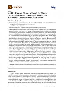
DESIGN OF ARTIFICIAL NEURAL NETWORK ARCHITECTURE FOR HANDWRITTEN DIGIT RECOGNITION ON FPGA THIẾT KẾ KIẾN TRÚC MẠNG NƠ RON NHÂN TẠO ỨNG DỤNG NHẬN DẠNG CHỮ SỐ VIẾT TAY TRÊN FPGA Huynh Viet Thang Danang University of Science and Technology, The University of Danang, VIETNAM Email:
[email protected] Tóm tắt – Bài báo này trình bày việc thiết kế và thực hiện một kiến trúc lõi IP mạng nơ-ron nhân tạo 2 lớp ứng dụng cho hệ thống nhận dạng chữ số viết tay trên FPGA. Chúng tôi sử dụng định dạng số dấu phẩy động bán chính xác với 16-bit để biểu diễn các trọng số của mạng nơ-ron. Mạng nơ ron nhân tạo được tổng hợp và kiểm tra trên FPGA Virtex-5 XC5VLX-110T, chiếm 41% tài nguyên phần cứng FPGA và có tần số hoạt động tối đa là 205 MHz. Khi thực hiện kiểm tra trên board mạch FPGA với 10,000 mẫu từ cơ sở dữ liệu chữ số viết tay MNIST, tỉ lệ nhận dạng đúng là 90.88% và thời gian nhận dạng là 8 (µs) cho mỗi mẫu. Các kết quả thực nghiệm cho thấy rằng lõi IP mạng nơ-ron nhân tạo được thiết kế trong bài báo rất phù hợp cho các ứng dụng nhận dạng mẫu trong các hệ thống nhúng. Từ khóa – mạng nơ ron; dấu phẩy động bán chính xác; MNIST; FPGA; tính toán hiệu năng cao; nhận dạng chữ số viết tay;
1. Introduction Artificial neural network (ANN) has many applications in signal processing and pattern recognition. ANN architectures demand a huge amount of parallel computing operations. To meet the demanding requirements for speed in real-time and high-performance computing (HPC) applications, ANN has to be implemented on parallel computing platforms like field programmable gate arrays (FPGA). This paper aims at addressing this issue. Neurocomputer building is expensive in terms of development time and resources [1], yet hardware development of ANN is actively carried out in recent years [2-5]. One of the main challenges for efficient implementation of ANN on FPGA is the data representation for the weights and transfer function. Dating back in 1991, Holt and Baker [6] studied the possibility of using fixed-point arithmetic for weight representation in ANN and showed that the 16-bit fixedpoint format can potentially be the typically chosen number format. Nichols et al. [7] examined the feasibility of using floating-point arithmetic for FPGA based neural network implementations through a classic logic-XOR problem. Savic et al. [8] has investigated the impact of number representation on implementing multilayer perceptron neural networks on FPGAs. In [9, 10], the twolayer feed-forward neural networks, employed fixed-point numbers, have been developed and implemented on FPGA. Recently, authors in [11] has found that reducedprecision floating-point numbers is a feasible choice for the implementation of neural networks on FPGA and showed that an optimal number format for single-FPGA implementation of ANN is the 16-bit half-precision floating-point number. In this work, we aim at achieving efficient FPGAimplementation of ANN applied for a handwritten digit
Abstract – This paper presents the design and implementation of a 2 layer feed-forward artificial neural network intellectual property (IP) core applied for handwritten digit recognition system on FPGA. We use 16-bit half-precision floating-point number format to represent the weights of the designed neural network. The neural network is synthesized and verified on Xilinx Virtex-5 XC5VLX-110T, occupies about 41% of FPGA hardware resources and can run at a maximal clock frequency of 205 MHz. When verified on the FPGA board with 10,000 samples from MNIST handwritten digit database, the recognition rate of the designed network is 90.88% and the recognition time is reported as 8 (µs) per sample. Experimental results show that our designed neural network IP core is suitable for embedded pattern recognition applications. Key words - neural network; floating-point; half-precision; MNIST; FPGA; high performance computing; handwritten digit recognition;
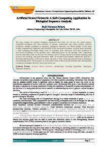
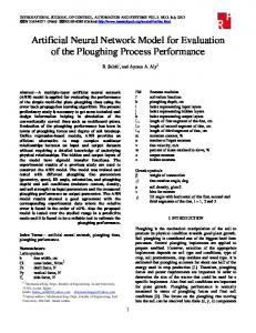
recognition system. We assume that the learning phase has been carried out on computers and, therefore, only focus on the FPGA implementation of the forward computation in the recognition phase of neural networks. The contribution of this paper is as follows. We will present the design, implementation and verification of a 2layer feed-forward artificial neural network architecture on Xilinx Virtex-5 XC5VLX-110T FPGA board. The network architecture is specified with VHDL and the weights are represented in 16-bit half-precision floatingpoint format [12]. The designed ANN is then used to classify handwritten digit images from the well-known MNIST database [13]. To our knowledge, we are the first to investigate the feasibility of FPGA-implementation of ANN for handwritten digit recognition with MNIST database using floating-point format. The rest of this paper is organized as follows. Section 2 briefly gives the system overview. Section 3 presents the design of a 2-layer artificial neural network architecture with only 22 neurons for handwritten digit recognition. Section 4 reports synthesis and verification results of the recognition system on the Xilinx Virtex-5 FPGA. Finally, we conclude the paper and sketch out some ideas for future work in Section 5. 2. System overview An overview of the proposed recognition system is presented in Fig. 1. The system consists of two main functional units: i) a feature extraction unit using principal component analysis (PCA) technique for dimensional reduction and ii) an artificial neural network (ANN) for recognition. 2.1. Handwritten digit database In this work, the MNIST database [13] is used as the data set for training and testing the neural network. The
Huynh Viet Thang
208
Fig. 1. Proposed recognition system based on artificial neural network
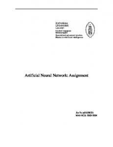
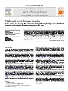
Fig. 2. Representation for half-precision (16-bit) floating-point number format in FloPoCo library
MNIST database offers a training set of 60,000 samples, and a test set of 10,000 samples. There are 10 different handwritten digits ranging from 0 to 9 in the MNIST database. Each digit is normalized and centered in a graylevel image of size 28x28, resulting in 784 pixels in total as the features. We applied PCA to extract the principal components from the original data and use only some first principal components as the extract features for training and testing the neural network classifier. 2.2. Training of artificial neural network for handwritten digit recognition We use a 2-layer feed-forward neural network to perform the recognition task. The designed network has 10 neurons in the output layer, corresponding to 10 types of output digits. We choose to use a 20-12-10 network configuration [11] (i.e., 20 principal components as inputs, 12 hidden neurons, 10 output neurons) for the implementation of neural network architecture on the Virtex-5 FPGA. The training of neural network for handwritten digit recognition system with MNIST database is carried out in MATLAB with the Neural Network Design Toolbox [14]. After training, we obtained the optimal weights and biases for the two layers of the design network. To make it convenient for the hardware implementation on FPGA, we consider the bias of each neuron as a special weight corresponding the “1” input. This results in two optimal weight matrices which will be used later for hardware implementation of the network, as follows: W1 (size: 12x21) is the weight matrix for the hidden layer, and W2 (size: 10x13) is the weight matrix for the output layer. 2.3. Weight representation To represent the weights of the network, we choose to use the half-precision floating-point number format [11], which showed that a reduced-precision floating-point format with 10 fraction bits can offers the same recognition performance as provided by a full-precision (double-precision) floating-point format on computer. The IEEE-754 standard [15] features the half-precision floating-point format with 1 sign bit (s), 5 exponent bits (e) and 10 fraction bits (f), or 16 bits in total. The halfprecision format allows for saving of 2X and 4X the registers (memory) for weight storage compared to the single-precision (32 bits) and double-precision (64) ones.
FloPoCo representation of the half-precision floating-point format will, therefore, have 18 bits in total, as shown in Fig. 2. The meaning of the exception field is as follows: “00” for zero, “01” for normal numbers, “10” for infinities, and “11” for NaN (Not-a-Number). As a result, all the datapaths will be 18-bit wires in VHDL implementation of the neural network.
The implementation of half-precision operators is based on the FloPoCo library [12]. Since the FloPoCo library uses 2 more bits for the exception field; the
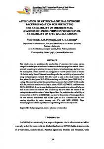
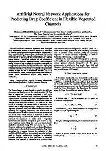
3. Design of 2-layer artificial neural network on FPGA In this section, we present the design and implementation of a 2-layer feedforward neural network architecture for the handwritten digit recognition application (see Fig. 3). We name the designed neural network architecture as the ANN IP core (IP – Intellectual Property). The general block diagram of the ANN IP core is given in Fig. 3a. The network consists of two layers with the same logic architecture. The differences between the two layers are the number of inputs, the number of neurons and the corresponding weights for each neuron in each layer. Optimal weight matrices W1 and W2 are constants and can be stored in ROMs. Similarly, the generic architecture of each neuron is the same, only weights of different neurons are different. We then only need to specify the architecture of one neuron and generate multiple copies of it with appropriate weights. 3.1. Architecture of one neuron Given the weight matrix W of size MxN and input vector x = [x1, x2,..., xN] of length N. The output ri of the ith neuron is computed sequentially by equations (1) and (2): 𝑁
𝑡𝑖 =
𝑤𝑖,𝑗 . 𝑥𝑗 𝑗 =1
𝑟𝑖 = 𝑓 𝑡𝑖 =
1 1 + 𝑒 −𝑡 𝑖
(1) (2)
where: ti is the net weighted sum of the i-th neuron; f (ti) is the log-sigmoid activation function (transfer function) of the neuron. Expanding equation (1) for all neurons in the layer, we can obtain the computation for the net weighted sum for one layer in a matrix-vector form as shown by equation (3). 𝑤1,1 𝑤1,2 … 𝑤1,𝑗 … 𝑤1,𝑁 𝑥1 𝑡1 𝑤2,1 𝑤2,2 … 𝑤2,𝑗 … 𝑤2,𝑁 𝑥2 𝑡2 ⋮ ⋮ ⋮ ⋮ ⋮ (3) … 𝑤𝑖,𝑗 … 𝑤𝑖,𝑁 . 𝑥𝑗 = 𝑡𝑖 𝑤𝑖,1 𝑤𝑖,2 ⋮ ⋮ ⋮ ⋮ ⋮ 𝑤𝑀,1 𝑤𝑀,2 … 𝑤𝑀,𝑗 … 𝑤𝑀,𝑁 𝑥𝑁 𝑡𝑀
209
ISSN 1859-1531 - TẠP CHÍ KHOA HỌC VÀ CÔNG NGHỆ ĐẠI HỌC ĐÀ NẴNG - SỐ 11(108).2016, Quyển 2
Obviously, the net weighted sum ti of the i-th neuron is the dot-product between the input vector x and the i-th row-vector wi = [wi,1, wi,1,…,wi,N] of the weight matrix W. The output column vector r = [r1, r2,..., rM]T of the entire layer is calculated by applying the log-sigmoid activation function in a component-wise manner to the net weighted sum vector t = [t1, t2,..., tM]T. For computing the net weighted sum of one neuron, we use a Multiply-Accumulate (MAC) operation, whose architecture is presented in Fig. 3b. The MAC unit consists of a multiplier, an addition and a DFF (D flipflop). The MAC unit performs the dot-product between two vector - the input vector x and the weight vector wi – in a sequential manner. For the implementation of the activation function, we combine three operations – an exponential, an addition and an inverse - to perform the log-sigmoid function as shown by equation (2). The hardware structure for the log-sigmoid operation is specified in Fig. 3c. The proposed architecture of one neuron is showed in Fig. 3d. Having implemented equations (4) and (5) by the MAC and log-sigmoid operations, we connect these two operations to perform the computation for one neuron of the network. The weight vector of the neuron is stored in ROM. In order to save FPGA resources, we reserve only 32 18-bit positions in the ROM in the current design, allowing for the execution of half precision floating point dot product of vectors with maximum length of 32 elements. 3.2. Architecture of whole ANN IP core Fig. 3e presents the architecture of the ANN IP core that performs the functionality of a 2-layer feedforward neural network for the handwritten recognition system based on MNIST database. We developed MATLAB scripts that allow for VHDL code generation of neuron and network layer specifications, given the optimal weight matrices. We generated 12 neurons in the hidden layer and 10 neurons in the output layer. The content of ROM in each neuron is the corresponding weight vector extracted from the optimal weight matrices W1 and W2. Since the inputs for one layer are arranged in series, we place a Parallel-to-Serial (P2S) unit between the two layers, the outputs of the network are then arranged in parallel, as shown in Fig. 3e. 4. Experimental result We use the Xilinx ISE tool 14.1 and the Virtex-5 XC5VLX-110T FPGA board [16] to synthesize and verify the ANN IP core implementation. The synthesis report is given in Table 1, showing that the network architecture occupies 28,340 slices out of 69,120 slices (41% of Virtex-5 FPGA hardware resources) and can run at a maximal clock frequency of 205 MHz. This report shows that the designed ANN IP core is suitable for embedded applications on FPGA. For verification and performance evaluation of the designed neural network, we build an embedded system on Virtex-5 FPGA board based on the soft-core 32-bit MicroBlaze microprocessor of Xilinx and add the ANN
a. General block diagram of the ANN IP core
b. Multiply-Accumulate (MAC) operation
c. The log-sigmoid operation
d. Architecture of one neuron
e. Architecture of the whole ANN IP core Fig. 3. Design of 2-layer artificial neural network on FPGA
Huynh Viet Thang
210
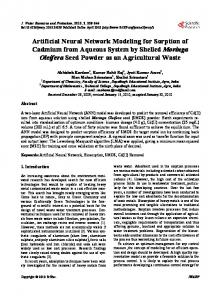
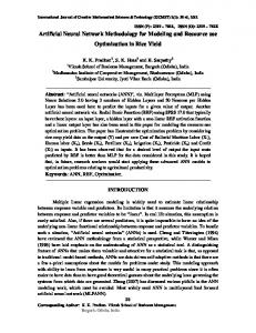
Fig. 4. Verification and performance evaluation of ANN IP core for MNIST handwritten digit recognition on Virtex-5 FPGA
IP core into the system via the PLB bus (PLB - Processor Local Bus). The MicroBlaze runs at a clock frequency of 100 MHz and features a serial interface (UART) which is connected with computer for data transfer and result display. We use this system to perform the handwritten recognition problem with MNIST images. The feature extraction with PCA technique is performed on computer using MATLAB for having 20 first principal components; these 20 principal components are then transmitted via UART to FPGA board for the ANN IP core to conduct the recognition task. The system is described in Fig. 4. Table 1. Synthesis results of ANN IP core on Virtex-5 FPGA Parameter
Value
FPGA device
Virtex-5 XC5VLX-110T
Max. frequency
205 MHz
Area cost
28,340 slices out of 69,120 (41%)
We use 10,000 test samples from MNIST database for the performance evaluation on the hardware board. The recognition rate reported by ANN IP core running on the Virtex-5 FPGA is 90.88 (%). The recognition time for one handwritten digit sample of ANN IP core is reported as 800 clock cycles, equivalent to 8 (µs) at the system clock rate of 100 MHz. Compared to other FPGA implementations of neural network in [9, 10], our ANN IP core outperforms others in terms of network size, recognition rate and execution performance. We also run the recognition of 10,000 MNIST test samples in MATLAB using the same configuration (same optimal weights), which reported a recognition rate of 91.33 (%). Compared to MATLAB implementation with 64-bit double-precision floating-point number format, the ANN IP core can provide quite accurate recognition results although it only uses 16-bit half-precision floatingpoint number format. The MNIST recognition rate reported on PC is about 95-99% [13] for different methods including using neural network classifiers, which is much higher than the
recognition rate (90.88%) of ANN IP core on FPGA board. For example, a recognition rate of 95.3% reported in [13] for MNIST database is obtained by using a 2-layer neural network with 300 hidden neurons. Meanwhile, the ANN IP core implemented on FPGA has only 12 hidden neurons (with only 22 neurons in total) and consumes much less power than a PC. Therefore, we believe that the proposed ANN IP core is a very promising design choice for high performance embedded recognition applications. 5. Conclusion We have presented the design, implementation and verification on FPGA of a 2-layer feed-forward artificial neural network (ANN) IP core for handwritten digit recognition on the Xilinx Virtex-5 XC5VLX-110T FPGA. Experimental results showed that the designed ANN IP core is very potential for high performance embedded recognition applications. Future work will focus on i) improving performance of the neural network and ii) extending the neural network to other recognition applications like face- and/or fingerprint recognition. Acknowledgment The author would like to thank Nguyen Thi Kim Anh and Nguyen Truong Tho for their great supports in this project.
References [1] Fernando Dias, Ana Antunes, Alexandre Mota, Artificial neural networks: A review of commercial hardware, Engineering Applications of Artificial Intelligence, Volume 17, Issue 8, December 2004, Pages 945-952, ISSN 0952-1976.. [2] Janardan Misra, Indranil Saha, Artificial neural networks in hardware: A survey of two decades of progress, Neurocomputing, Volume 74, Issues 1–3, December 2010, Pages 239-255. [3] IBM Research: Neurosynaptic Chips: http://research.ibm.com/cognitive-computing/neurosynapticchips.shtml#fbid=U7U04FvCvJW [4] General Vision: Neural Network Chip: http://generalvision.com/cm1k/ [5] C. Shi et al., "A 1000 fps Vision Chip Based on a Dynamically Reconfigurable Hybrid Architecture Comprising a PE Array Processor and Self-Organizing Map Neural Network," in IEEE Journal of Solid-State Circuits, vol. 49, no. 9, pp. 2067-2082, 2014 [6] J. L. Holt and T. E. Baker, "Back propagation simulations using limited precision calculations," IJCNN-91, IEEE, Jul. 1991. [7] K. R. Nichols, M. A. Moussa, and S. M. Areibi, "Feasibility of Floating-Point arithmetic in FPGA based artificial neural networks," in In CAINE, 2002, pp. 8-13. [8] W. Savich, M. Moussa, and S. Areibi, "The impact of arithmetic representation on implementing MLP-BP on FPGAs: A study" IEEE Trans. on Neural Networks, vol. 18, no. 1, pp. 240-252, 2007. [9] M. Hoffman, P. Bauer, B. Hemrnelman, and A. Hasan, "Hardware synthesis of artificial neural networks using field programmable gate arrays and fixed-point numbers," in R5 Conference, 2006 [10] S. Hariprasath and T. N. Prabakar, "FPGA implementation of multilayer feed forward neural network architecture using VHDL," 2012 ICCCA, Dindigul, Tamilnadu, 2012, pp. 1-6. [11] T. Huynh, "Design space exploration for a single-FPGA handwritten digit recognition system," in IEEE ICCE, 2014 [12] FloPoCo code generator: http://flopoco.gforge.inria.fr/ (last accessed Sep 26, 2016) [13] MNIST http://yann.lecun.com/exdb/mnist/ (last accessed Sep 26, 2016). [14] Neural Network Toolbox™ 7 User’s Guide. [15] “IEEE standard for floating-point arithmetic,” IEEE Std 754-2008. [16] www.xilinx.com (last accessed Sep 26, 2016).