he problems of testing increasingly complex digital integrated .... The JTAG instruction-register path is implemented in the IC-level ..... and signature analysis.
DESIGNING AND IMPLEMENTING
AN ARCHITECTURE
WITH BOUNDARY SCAN
R.P. VAN RIESSEN H.G. kERKHOFF A. KLOPPENBURG University of Twente, The Netherlands The authors describe a standardized, structured test methodology based on the boundary-scan proposal from the Joint Test Action Group, which is now IEEE proposed standard P1149.1.The architecture ensures testability of the hardware from the printed-circuit- board level down to integrated-circuit level. In addition, the architecture h a s built-in self-test a t the IC level. The authors have implemented this design using a self-test compiler.
FEBRUARY 1990
.
he problems of testing increasingly complex digital integrated systems continue to challenge the design and test community. At the printed-circuit-board, or PCB, level, these problems led to the formation of JTAG, short for Joint Test Action Group, a collaborative organization of major semiconductor users in Europe and North America. JTAG subsequently developed the boundary-scan standard' with the goal of improving the controllability and observability of an IC's primary inputs and outputs. Because of this standard, which is now IEEE proposed standard P1149.1, we can now easily implement testability hardware using computer tools, which reduces overall design time.
T
However, boundary scan does not address testability at the IC level-primarily because there is no standard for designing BET circuits. At this level are many approaches to adding testability, but the one that seems most promising for future VLSI and ULSI circuits is built-in self-test, or In BIST, test data is generated and evaluated on the chip. In this article, we present an architecture called hierarchical testable, or H-testable, architecture for integratingboundary scan at the PCB level and BIST at the IC level. We believe that this integration is important because the boundary-scan standard defines access to the IC during the IC test. The extra test pins let u s control on-chip testability hardware. A digital system has several levels of hierarchy. First, we have the PCB level, which contains such items as a Winchester control board. The second level is the IC level, where we have units such as a microprocessor chip. The third level, called the macro level, allows us to make finer distinctions between functional modules like PLAs and &Us, for example-the so-called macros3 We use these three levels to define the H-testable architecture. With this hierarchical structure, we can use BIST for a macro at the higher levels and so more completely integrate the testability features at the IC and PCB levels. As we show in more detail later, the H-testable architecture can be implemented using a self-test ~ o m p i l e rThis . ~ compiler automatically generates the layout of a macro, including hardware to generate data for and evaluate the results of self-test. 0740-7475/9O/0002-09$1.ooO199O IEEE
9
CHIP-LEVELSELF-TEST Test interface elements are located at the primary inputs and outputs of both macros andICls. Each TIE contains boundary-scan cells and serial control registers.
ARCHITECTURAL REQUIREMENTS To be H-testable, an architecture must have certain characteristics. First, it must be hierarchical because, as we just mentioned, the hierarchical approach allows us to use test results from a lower level in higher levels. The results of a macro test can be used for the IC test, for example. Second, the architecture has to be standard because PCB manufacturers use ICs from different vendors on a single board. If we have well-defined test-interface rules and control definitions for every level of hierarchy, we can use standard test approaches. Third, the architecture has to be structured also to reduce extra design time. With a structured approach, test hardware is developed only once and is reusable. A structured approach also facilitates the design by allowing u s to use computer tools. Finally, to be H-testable, the architecture must incorporate the BIST facilities of different macros.
INTEGRATION WITH BOUNDARY
SCAN Figure 1 shows the JTAG boundary-scan architecture for PCB testing. The behavior and architecture of all blocks in this figure are defined in the standard.' We use this architecture to define our H-testable architecture. Figure 2 is a schematic block diagram of the H-testable architecture at the IC level. In this diagram, we can distinguish two levels of hierarchy: the macro level and the IC level. At the IC level are (self-)testablemacros, connections between these macros, and additional testability hardware. The macro level consists of a (self-)testable macro with additional testability hardware. Both levels of the testability hardware incorporate test interface elements, or TIEs; a test processor; and a scan path. The TIEs separate a macro (IC) from the connections with other macros (ICs).Therefore, TIEs are located at the primary inputs and primary outputs of both macros and ICs. Each TIE contains boundary-scan cells and serial control registers. Test processors provide parallel control of the TIEs.
- Boundary-scan path I - User-defined registers - Multiplexer Bypass m TDI
I
1
-N DR select
I Select Enable
TCK
controller
I
Status I
I
I
Figure 1 . Architecture of the Joint Test Action Group boundary-scan standard.
IEEE DESIGN & TEST OF COMPUTERS
10
T
The IC test processor provides the TIEs at the IC level and the macro test processors with parallel control. The macro test processor provides the TIEs at the macro level with parallel control. The macro test processor can also control a macro self-test.
ARCHITECTURE AT THE IC LEVEL At the IC level, the H-testable architecture is compatible with the boundary-scan architecture and its behavior. Therefore, we have in effect merged the H-testable architecture with the JTAG boundaryscan architecture as evidenced by the following structural characteristics:
We can merge theJTAG boundary-scan and H-testable architectures without any changes to either. Thus, the H-testable architecture is already defined at the IC leuel.
The JTAG boundary-scan path in Figure 1 is part of the boundaryscan cells of the TIEs at the IC’s input and output in Figure 2. The JTAG instruction-register path is implemented in the IC-level test processor. The registers in this path provide the serial control data for the IC-level TIE. The JTAG test-access port (TAP) controller is implemented in the IC-level test processor of the H-testable architecture. The TAP controller generates the parallel control signals for the IC-level TIEs and the macro-level test processors. The JTAG user-defined register path is used to implement the local scan path in Figure 2. We can merge the architecture of the JTAG boundary-scan standard and the H-testable architecture without any changes to either. Consequently, at the IC level, the H-testable architecture has already been defined.
ARCHITECTURE AT THE MACRO LEVEL The test hardware for the H-testable architecture at the macro level consists of TIEs and a macro test processor, as Figure 2 shows. A TIE in the local scan path forms the link between a macro and the macro interconnection. We add this element only to enhance testability. The TIEs are located at both inputs and outputs of a macro and do not affect the functional behavior of the IC during normal operation.
Test processor
Test processor
Local scan path .---------_-______________ Parallel control
--
I
TMS TCK TDI
IC-level test processor
TDO
4
IC-level TIE
1......._.._...... 1 IC out
.................
IC in
Figure 2. Block diagram of the hierarchical testable @f-testable)architecture at the IC level. FEBRUARY 1990
11
CHIP-LEVELSELF-TEST Data-register cells form the i n w a c e of the mucro and mucro interconmctitms. DRC modes vary according to the control signuls afilied to the multiplexers.
During an IC test however, the TIEs are able to separate macros from their interconnections, which allows an independent test of both. Test patterns are shifted serially into the TIE via the local scan path, and the TIE applies the patterns in parallel to the macro or to the interconnection of macros. Results from a macro self-test are loaded in parallel into the TIEs at the output of the macro. Results from the macro interconnection test are loaded in parallel into the TIEs at the input of a macro. Next, data m the TIE’Swill be shifted out serially via the local scan path. Control signals for the TIE are applied serially via the local scan path and in parallel via the control signals from the macro-level test processor. Figure 3 shows the implementation of the TIE. A TIE consists of data-register cells D, two control-register cells ( M and S), a bypass path, and a multiplexer. Data-register cells form the interface of the macro and the interconnections to other macros. Figure 4a is a block diagram of one of these cells. This cell consists of two multiplexers and a master-slave register. The macro-level test processor provides the signals Mode, DRC1, and DRC2. The data-register cell is used in different modes, which vary according to the control signals applied to the multiplexers. Figure 4b shows the truth table of multiplexer 2. The first mode
L
I
01
Instruction path TDO 1 2 - M S -
o 4n .-
figure 3. Implementationof a test interjime element, or TIE: D is the data-register cell and M and S are control-register cells.
-
Data in ,-0
5
01 -
n
1 .z
cu
r’
~
Data out
Hold
0)
MSFF
(1
3 NormalE - Test-
I! I 0
Hold Test NiFtal
S h i f t 7
1-f-e
fa)
Test
0
TCK DRC1 DRC2
I
TDI
figure 4. Block diagram of a data-register cell data-register multiplexer 2 &I.
(4and the truth table for
IEEE DESIGN & TEST OF COMPUTERS
12
--7
of the data-register cell is the hold mode (DRC1=0,DRC2=O),in which data in the register remains unchanged. The second mode (DRC1=1, DRC2=O) is the test mode, in which the input Test is used for BIST. The third mode (DRC1=0, DRC2=1) is the scan mode, in which the cell is placed in the local scan path at the IC level. Figure 2 shows this path. We can now shift data into input TDI and towards output TDO. The fourth mode (DRC1=1,DRC2=1)is the normal functional operation. Data enters the cell via the input Data-In and propagates through the cell with minimal delay to Data-Out.
At the PCB level, the F A G boundary-scan architecture requires two scan qPeratiolts to initiute the test interface elements: ship in instruction bits and ship in datu bits.
The control-register cells in the instruction path of a TIE (Mand S in Figure 3) provide its serial control. These registers consist of a shift register (L2) and an output latch (Ll). Figure 5a is a block diagram of an instruction-register cell. The TAP controller of the IC-level test processor supplies the control signals Update-IR, IRC 1, and IRC2. At the rising edge of Update-IR, the contents of shift register L2 are loaded into the output latch L1. The signals IRC 1 and IRC2 control which input is selected by the multiplexer. Figure 5b shows the truth table of this multiplexer.The input Hold (IRC1=0,IRC2=0)is selected to retain the data in the output latch L1. The input Status (IRC1= 1, IRC2=O)is required to load a signal into the shift register. The input Shift (IRC1=0/1, IRC2=1) is the serial scan input. This input is connected to the output TDO of the previous shift-register cell. Because TIEs are at both the input and output of a macro, there are two mode registers-M1 at the input, M2 at the output-and two select registers41 at the input and S2 at the output. These four instruction registers can define 16 modes for the data-register cells. The select register S in Figure 3 controls the bypass of the dataregister cells. The data-register cells in a TIE are placed in the local scan path if S=l. If S=O the scan path of a TIE contains only the instruction-register cells. The value in the mode register M is decoded in the macro-level test processor and, together with parallel control signals from the IC-level test processor, controls the two functions of the data-register cells. In Figure 4a the data-register cells transmit data if mode=l and receive data via input Data-In if mode=O.
-
Figure 3 shows, in contrast with the JTAG architecture, that the boundary-scan path and the instruction path are connected serially. With this architecture at the macro level, we can use a simple multiplexer to select either the bypass mode or the boundary-scan mode. Because both modes include the instruction path, a data scan will always contain data bits and instruction bits. We need only one scan operation to initialize the TIES for a macro test. At the PCB level, the JTAG boundary-scan architecture requires two scan operations to initiate the TIEs. In the first stage, the instruction bits are shifted in. In the second stage, the data bits are shifted in.
lRCl IRC2
I
1
IRC2
Another difference between the macro-levelTIE and the IC-level TIE is the number of modes that a data-register cell has. The boundaryscan data-register cell at the IC level has three modes of operation. At the macro level, it has four modes. As we mentioned earlier, this additional mode is the test mode, which allows the data-register cell to be used for BET. This mode does not require an extra control signal as compared with the boundary-scan register cell. FEBRUARY 1990
Hold Multiplexer Status
D Latch Out
-
TDI- Shift
IRCI
L2 MSFF -
&
>
I
Selected Input Hold Status Shift Shift
figure 5. Block diagram of an instructionregister cell (4and the truth table for the instruction-register multiplexer (b).
13
CHIP-LEVELSELF-TEST Central to the H-testable architecture is the sey- testable macro, which has only combinational logk.
THE MACRO-LEVEL TEST PROCESSOR The test processor forms the control part of the H-testable architecture. At the macro level, the processor has to perform a macro self-test and apply the parallel control signals to the data-register cells of the TIES at both the input and output of the macro. To carry out BIST, we must generate test patterns and compact them using some hardware implementation of a test-pattern generation/compaction algorithm. Test patterns are applied in parallel to the macro inputs by loading the test patterns in the data-register cells via the extraTest input, as Figure 4a illustrates. The test result is loaded in parallel into the TIE at the output of the macro. During the self-test, the macro test processor generates the parallel control signals for the data-register cells of the TIE. Figure 6 is
s2
-1
BSH-dr BAH-dr
Self-test Ready
Decoder
=I
Controller
-f
Pattern generator
Dataout
Parallel control
I
*
DRC22 Model Mode2
Figure 6 . Block diagram of a macro-level test processor:
TCK, IRCl, IRC2
Data in
r
0
E v)
0 3 W
-0
% 3
TCK, IRCI, IRC2
Out [ l ...41
Figure 7. Example of the hierarchical testable, or H-testable architecture. IEEE DESIGN Ut TEST OF COMPUTERS
14
---
T
a block diagram of the macro-level test processor. We briefly describe the main parts of the test-processor architecture. A more detailed description is available el~ewhere.~ Parallel and serial control logic supply the data-register cells with control signals. The signals DRCl1, DRC12, and Model form the signals DRC 1, DRC2, and Mode for the TIE at the input of a macro. The signals DRC21, DRC22, and Mode2 form the signals DRC1, DRC2, and Mode for the TIE at the output of a macro. These signals
A pattern gemraw, which is governed by the controller, generates the testpatterns for the macro.
AN H-TESTABLE ARCHITECTURE The best way to illustrate the features of the H-testable architecture is to describe an actual implementation. Figure 7 shows the example we have used. Our intent is primarily to show the integration of
boundary-scan hardware with BIST at the IC level. Our example incorporates two TIEs, a macro test processor, one TAP controller, and a simple macro. The central part in the architecture is the self-testable macro, which has four inputs and four outputs. This macro contains only combinational logic and is tested with pseudorandom patterns. A signature analyzer compacts the test results. We have added some hardware to the data-register cells of the TIEs so that we can use the data register as a building block for pseudorandom pattern generation and signature analysis. Figure 8 illustrates the additional hardware. We form the pattern generator/compactor by connecting a number of modified data-register cells as a linear-feedback shift register. To do this, we feed Data-Out ofthe last register cell back to the Feedback terminal of specific data-register cells. The connections are determined by the feedback polynomial.6We can use the structure as a pseudorandom pattern generator when (DRC1, DRC2)=(1.0) and mode=l. The circuit operates as a signature analyzer when (DRC1, DRC2)=(1,O)and mode=O. In our example, the TIEs form an LFSR during the test mode that has a feedback polynomial of l+X+2. Figure 9 shows the data register of a TIE realizing this LFSR. The macro-level test processor also incorporates the logic to start and complete the self-test. The Ready signal, which indicates the completion of the self-test, is true when a specific test pattern is generated. FEBRUARY 1990
15
CHIP-LEVELSELF-TEST We have added some hardware so that we can use the data regktkr as a building block for pseudorandompattern generation and signuture analysis.
Data in-
0
-Data out
Multiplexer
~
Mode
Figure 8 . Block diagram of a modifid data register.
: I
TCK Mode DRC1DRC2-
1 I
I
-
l
l
I
I 11
I
I
l l
-
rd
I
I
I
Multiplexer 1
I
-
I
Multiplexer 2 TDO
TDI
Shft Data out
Figure 9. Block diagram of the data register part of the test interface element. or TIE, that forms afour-bit linearfeedback shijl register withfeedbackpolynomial 1 +X+x'. IEEE DESIGN & TEST OF COMPUTERS
16
T
The TAP controller is identical to the TAP controller as described in version 2.0 of the boundary-scan standard.'
SIMULATION OF THE SAMPLE CIRCUIT Table 1 shows the scan actions applied to the example circuit during simulation. Scan action 1 initializes the instruction-register cells. Four clock cycles shift the values for the initialization path into the instruction-register cells: (Ml,Sl,M2,S2) = (1,1,0,1). Because S1= 1 and S2=1, we can initialize the data-register cells at both the input and output. Scan action 2 initializes the data-register cells for a macro self-test. Both data-register cells are initialized with the value (1,l,O,O). Scan action 3 indicates that during a macro self-test, we can still shift data through the TIEs. While the two TIEs perform a macro self-test, a pattern is shifted via the input TDI to the output TDO. We need scan action 4 to place the data-register cells in the scan path after the macro self-test has been completed. Finally, with scan action 5, the signature in the output TIE appears at the serial output TDO. We simulated the test process for this sample circuit using a 7 switch-level description. The results of the simulation5 show the correct operation of the H-testable architecture. A layout for the individual blocks of the H-testable architecture has since been designed and will be used in our self-test compiler.
With the self-test comfiilq designers define only the type and size Ofthe mucro to be realized and thefault coverage they desirefor the self-test.
A SELF-TEST COMPILER As we mentioned earlier, the purpose of the H-testable architecture is to develop a standard, hierarchical test approach to ease the burden of test development. Towards that end, we implemented our architecture in a self-test compiler.* The compiler automatically generates the layout of the most appropriate on-chip test hardware for self-testing along with the functional macro. Designers define only the type and size of the macro to be realized, along with the fault coverage they desire for the self-test. Using the described architecture, the compiler generates self-testable macros that we can control in a standardized format. The H-testable architecture defines the signals to initialize, control, and verify a macro self-test from the macro level to the PCB level.
Table 1 . Tests applied to the sample circuit in Figure 9.
No.
Scan Action
M1
Instruction S1 M2 52
1
Select initialization path
1
1
0
1
2
Initialize dataand instruction register
1
0
0
0
3
Scan operation during self-test
1
0
0
0
4
Select result path
0
1
0
1
5
Verify test result and scan in pattern for external test
0
1
1
1
FEBRUARY 1990
17
CHIP-LEVELSELF-TEST For small mucros of say, 10 to 20 I/O ports, the controllers will probably determine the ouerhead of the extra test hardware.
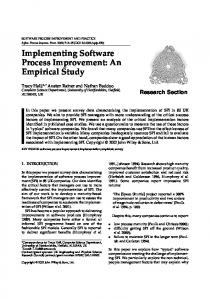
Figure 10 shows part of the layout of a self-testing carry-save array multiplier, which was generated by the self-test compiler. The selftest, performed in this particular structure, is an exhaustive test. We used a signature analyzer to evaluate the test responses. The bottom row of cells in the figure shows the layout of some data-register cells used for data compaction. The overhead needed for the extra test hardware vaies with the size of the array multiplier. For a 16x16-input carry-save array multiplier, for example, the overhead is about 20%. For a 32x32-bit array multiplier, the overhead is about 12%. he H-testable architecture we have described will ease the problems of testing ICs on printed-circuit boards. I t is hierarchical, structured, and compatible with the JTAG boundary-scan standard for PCB testing. Using this architecture, we can initialize, control, and verify a macro self-test from the IC level up to the PCB level. During a macro self-test, the IC-level scan path can still be used, which implies that we can test different macros in
T
Figure 1 0 . Part of the layout of a self-testingcarry-save array multiplier;which
was generated by the self-test compiler. The bottom row of cells shows the layout of some data-register cells used for data compaction. IEEE DESIGN
10
T
(It
TEST OF COMPUTERS
parallel with the H-testable architecture. We have implemented this architecture in a self-test compiler. An example circuit, generated by this compiler, shows the possibilities of this architecture. The overhead of the extra test hardware remains a Droblem that needs more research. For small macros of say, 10 to 50 1 / 0 ports, we expect the controller parts of the H-testable architecture to determine the overhead. Therefore, we advise the use of only one macro test processor for a set of small self-testable macros. @ ~~~~
~
Ronald P. van Riessen is working towards a PhD in at the ofTwente, Enschede, The Netherlands, where his research interests include automatic design for testabilitv and BIST of CMOS VLSI s%ems, PartiCuiarlY boundary Scan with
, " , OfTwente.
'
~
e
~
~
c
ACMVO WLEDGMENTS This research is supported by the Innovative Research Program (IOP) on IC technology under HTO-049/ 1, part testing. We thank F. Beenker and his group at Philips Research Laboratories, Eindhoven, for their contribution to this research.
Hans G* Kerkhoff is a staffmember Of the IC and Group Of the University Of Twente*where his interests are in testable CAD for VLSI digital signal processors. He holds an MSc in electronical engineering kom the Technical University of Delft and a PhD in microelectronicsdesign from the University of Twente.
REFERENCES 1. A Test Access Port and Bounday Scan Architecture,JTAG standard, Version 2.0, Draft 2, Jan. 1988. 2. B. Koenemann, "Built-In Logic Block ObservationTechniques," Proc. Int'l Test Con$, 1979, pp. 37-41. 3. F. Beenker et al., "Macro Testing: Unifying IC and Board Test," B E E Design & Test of Computers, Vol. 4, No. 6, Dec. 1986, pp. 26-32. 4. R. van Riessen, H. Kerkhoff and A. Kloppenburg, "Design of a Compiler for the Generation of Self-TestableMacros," Proc. European Solid-State Circuits CO&., 1988, pp. 194-197. 5. A. Kloppenburg, Investigations on the Possibilities of Using Boundary-Scan Techniques in Silicon,MSc thesis, Univ. of Twente, 060-700 1, Enschede, The Netherlands, July 1988. 6. A. Miczo, Dgital Logic Testing and Simulation.John Wiley & Sons. New York, 1987. 7. A. van Genderen, A. de Graaf, "SLS: A Switch-Level Timing Simulator," in The Integrated Design Book, Del!? Univ. Press, 1986, The Netherlands, pp. 2.932.145.
FEBRUARY 1990
Ad Kloppenburg is a staff engineer a t Witteveenen Bos, an engineeringconsultancy in Deventer, The Netherlands. He holds an MSc in electrical engineering kom the University of Twente.
Direct questions or comments on this article to R. van Riessen, University of Twente. EF Bldg., PO Box 217, 7500 AE Enschede, The Netherlands.
19
~
~
~
~