A high-performance new cell technology has been developed successfully with improving impurity distribution in shorter de- velopment time by using this system ...
IEEE TRANSACTIONS ON ELECTRON DEVICES, VOL. 44, NO. 10, OCTOBER 1997
1611
Device Design with Automatic Simulation System for Basic CCD Characteristics Keishi Tachikawa, Takuya Umeda, Yoshinori Oda, Member, IEEE, and Takao Kuroda
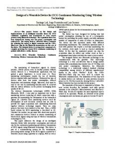
Abstract—A simulation system has been developed to automatically analyze basic electric characteristics of a charge-coupled device (CCD) image sensor from a process simulation result. This system shortened the simulation period to approximately 1/10 by getting rid of complicated repetitious procedures. A high-performance new cell technology has been developed successfully with improving impurity distribution in shorter development time by using this system. This technology has been realized as a CCD cell pixel with CCD charge quantity of 1.8 times, effective transfer efficiency of over 99%, no image lag for driving read-out pulse voltage in comparison with conventional technology. A 1/4-in 330 k square pixel progressive-scan CCD was fabricated with this technology. These results are described to demonstrate the effectiveness of the automatic simulation system. Fig. 1. Impurity concentration profile of unit CCD cell.
I. INTRODUCTION
R
ECENTLY, charge-coupled device (CCD) image sensors have been advanced by downsizing and increasing the pixel number to apply to small handy video cassette recorders (VCR) for consumer use and business use. In addition, progressive-scan CCD’s for multimedia have been greatly in demand in recent years [1]–[3]. A high-performance new cell technology corresponding to the reduction of pixel size is indispensable to the development of downsized CCD image sensors lately. Comprehensive cell design with process and device simulation is essential to realize this technology efficiently [4]. However, there are many important procedures (e.g., defining discretized mesh [5], setting electric contacts, and bias voltage, etc.) in device simulation to analyze electric characteristics correctly. Therefore, a simulator that analyzes electric characteristics of CCD’s easily and has a short manipulation time has been desired for everyone because it is difficult to analyze these characteristics for an engineer who is not an expert. This paper describes a two-dimensional (2-D) simulation system that analyzes basic electric characteristics of a CCD image sensor fully automatically from a process simulation result. By using this system, a high-performance new cell technology has been achieved, and the result was applied to a development of progressive-scan CCD. Manuscript received October 23, 1996; revised March 24, 1997. The review of this paper was arranged by Editor N. Teranishi. K. Tachikawa, Y. Oda, and T. Kuroda are with the ULSI Process Technology Development Center, Matsushita Electronics Corporation, Kyoto 601, Japan. T. Umeda was with the Kyoto Research Laboratory, Matsushita Electronics Corporation, Kyoto 601, Japan. He is now with the Semiconductor Advanced Technology Development Center, Matsushita Electric Industrial Co., Ltd., Osaka, Japan. Publisher Item Identifier S 0018-9383(97)06917-7.
This paper is organized as follows. Section II describes the automatic simulation system. A high-performance new cell design is presented and discussed in Section III. Finally, concluding remarks are given in Section IV. II. AUTOMATIC SIMULATION SYSTEM In a CCD image sensor, there are isolated insular n-type regions (CCD channel, photo diode) in a p-type region as shown in Fig. 1. It shows an impurity concentration profile of a unit CCD cell. Special treatment is needed in executing device simulation, because these regions are in an electrically floating state. To handle the structure, the authors used the following special treatment. After setting an electrode in the insular floating region and applying bias voltage, the electrode is removed and a steady state solution is solved. By using this method, high precision of simulation result can be obtained and operation time can be shortened during the simulation. However, in this method, even an expert of simulation must require many procedures in analyzing device characteristics, because there are many experiential laws in setting the electrode and bias condition, and sometimes different simulation condition (e.g., device structure, mesh, position of electrode, bias, etc.) lead to different steady state solutions. To overcome the above drawback, a simulation system has been developed that automatically generate discretized mesh, set electrodes, specify bias steps of the electrodes, and plot out required result. Analysis method and functions of this system are described in this section. A. Analysis Method of Automatic Simulation System A flow chart for the developed Automatic Simulation System is indicated in Fig. 2. An analysis procedure of the
0018–9383/97$10.00 1997 IEEE
1612
IEEE TRANSACTIONS ON ELECTRON DEVICES, VOL. 44, NO. 10, OCTOBER 1997
Fig. 3. Set minimum point of discretized mesh space in after extracting p-n junction line and silicon surface.
X, Y
direction,
where
Fig. 2. Flow chart for the developed Automatic Simulation System in case of read-out characteristic analysis.
system is explained according to this flow chart of read-out characteristics analysis for CCD image sensor as an example. 1) Generation of Impurity Structure for Device Simulation: Impurity structure for device simulation is automatically generated in the following procedure with a result of impurity distribution simulated from process simulator shown in Fig. 1. Each of the 2-D contour lines indicate equivalent concentration. Step 1: Check loaded impurity distribution and structure (e.g., position of gate electrode, existence of CCD channel, photo diode, etc.) shown in Fig. 1. Step 2: Define the device simulation region and generate a temporary impurity structure for device simulation. Step 3: Set a minimum point of discretized mesh space in , direction, after extracting p-n junction line and silicon surface indicated in Fig. 3. Mesh space close to the point in each split region is minimum to stabilize convergence of the simulation. By choosing the minimum point according to the above position, the minimum point corresponds to an abrupt potential gradient or high impurity concentration position automatically in the CCD structure. Step 4: Split each region in , direction at the minimum point decided in Step 3, as indicated in Fig. 4. Step 5: Calculate number of mesh , minimum space of mesh in each split region. 1) Decide number of mesh in each split region. Number of mesh is expressed as the next equation (1)
width of split th region; total width of split each region. In other words, it is equal to region size of simulation direction; in , total number of mesh; weight for dividing mesh of th region. It is decided based on data of structure recognition and experiential law; impurity concentration in one end of -th region; impurity concentration in the other end of -th region. Impurity concentration and the gradient at both edges and in each split region are very important factors weight to realize a numerically stable mesh in convergence. In our slightly big at CCD system, we choose set to channel, photo diode and between them. And at n-sub and gate terminal be relatively small region. in each split region 2) Decide minimum mesh space is expressed as the next Minimum mesh space equation (2) where number of mesh in th region; , , , , and are the same as in case of 1). Mesh space in each region is calculated to form a geometric . In this case, the number series with an initial value of of mesh is calculated from the above . If the ratio of the in this geometric series becomes greater than 1.5, weight region is automatically altered to decrease the calculation error and to stabilize convergence of simulation, then the number of mesh and the minimum space of mesh are calculated again. Fig. 5 shows discretized mesh generated automatically according to the procedure 1), 2). This method can generate fine discretized mesh at an abrupt potential gradient position and high impurity concentration region.
TACHIKAWA et al.: DEVICE DESIGN WITH AUTOMATIC SIMULATION SYSTEM
1613
TABLE I ANALYSIS FUNCTIONS OF THE AUTOMATIC SYSTEM. CHARACTERISTICS RELATED TO CCD CHANNEL, PHOTO DIODE, READOUT, AND BLOOMING ALL
OF SIMULATION
Fig. 4. Split each region in Step 3.
X, Y
direction at minimum point decided in
Fig. 5. Discretized mesh generated automatically with number of mesh minimum mesh space A0i by Automatic Simulation System.
ni , Fig. 6. Cross-sectional view of unit CCD cell.
Step 6: Put electrodes at each designated position (gate, CCD channel, etc.). Step 7: Calculate impurity distribution again on the generated mesh and electrode information for device simulation. 2) Execution of Device Simulation: In this part, the system calculates the read-out characteristic by transient analysis from the accumulated signal charge state as an initial condition, and plots out the results. Step 8: Solve steady state solution that has depleted CCD channel and accumulate signal charge in photo diode by applying bias condition to each electrodes. Step 9: Run transient analysis simulation for signal charge dependency of gate read-out voltage from the result Step 8: as an initial condition with no electrodes in CCD channel and photo diode. Step 10: Plot and print out specified parameters from the simulation result. B. Analysis Functions of Automatic Simulation System All of the analysis functions of the automatic simulation system are shown in Table I. This system realize an automatic analysis of characteristics related to the CCD channel, photo diode, read-out and blooming, thus efficient the CCD unit cell design will be accomplished effectively in a short development time.
III. DISCUSSION OF DESIGNING HIGH-PERFORMANCE CELL Design of a high-performance new cell has been studied that greatly improves saturation characteristics of the CCD channel mainly with low a temperature process. Generally speaking, improvement of saturation characteristics that need optimization of the structure of the gate insulator, CCD channel, and p-well just under the channel tends to lower transfer efficiency due to fringing electric field drop. In addition, read-out characteristics tend to be greatly affected by these structures. Based on this study, the authors proposed new cell technology to accomplish the increasing of CCD saturation charge quantity by extending effective channel width and raising impurity concentration in the CCD channel, and suppressing by shallowing the CCD channel and rising the p-well impurity concentration. Minimum potential in the depleted CCD channel , characteristics of saturation and readout was simulated in the cross-sectional region of the unit CCD pixel shown in Fig. 6 by the above-mentioned simulation system. Transfer efficiency was estimated by simulating the fringing electric field in the depleted CCD channel in the crosssectional region of the CCD transfer channel shown in Fig. 7. By optimizing the device structure with respect to transfer efficiency and read-out characteristics, high-performance new cell technology has been developed successfully.
1614
IEEE TRANSACTIONS ON ELECTRON DEVICES, VOL. 44, NO. 10, OCTOBER 1997
Fig. 7. Cross-sectional view of CCD transfer channel. Fig. 9. 1-D impurity distribution of new technology and conventional one along with the horizontal direction indicated in Fig. 6. TABLE II PROCESS CONDITION DEPENDENCE OF SATURATION CHARGE QUANTITY �min OBTAINED FROM SIMULATION AND MEASUREMENT
Fig. 8. 1-D impurity distribution of new technology and conventional one along with the vertical direction indicated in Fig. 6.
A. Improvement of CCD Saturation Characteristics, Suppression of Fig. 8 shows a one-dimensional (1-D) impurity distribution of the new cell technology and a conventional one along with vertical direction that indicate the cross-sectional view of the unit CCD cell in Fig. 6. Fig. 9 shows a 1-D impurity distribution of the new cell technology and a conventional one along with the horizontal direction indicating the crosssectional view of the unit CCD cell in Fig. 6. Increasing the effective total quantity of impurity and extending the effective width of the CCD channel is indispensable by increasing the CCD saturation charge quantity in order to increase the handling charge. Therefore, a high impurity concentration was proposed to the CCD channel by suppressing a diffusion from/into the CCD channel vertically as shown in Fig. 8. Also, an extension of the effective CCD channel width was proposed, that suppresses lateral diffusion of impurity from/into the CCD channel horizontally as shown in Fig. 9. (active impurity According to Gauss’s law, a potential (thickness of depleted concentration in depleted layer) part in the layer) , reduction of thickness in a depleted . Therefore, a layer strongly affects the suppression of shallow junction CCD channel and a high-dose p-well due to suppression of impurity diffusion was proposed. To realize the proposed new cell technology in CCD image sensor, a low temperature process was introduced.
Table II describes the concept of the above new cell technology as a process condition. It shows the condition dependence process of saturation charge quantity, obtained from simulation and measurement. Arrows in Table II depict the tendency of each characteristic by increasing the dose and energy for each ion implantation. The following two facts were clearly obtained from the result. 1) High-dose and low-energy P-implantation in the CCD channel drastically increase the CCD saturation charge quantity. 2) High-dose in the p-well just under the CCD channel affects the suppression of strongly. Device structure with this new cell technology was achieved with approximately 1.45 times larger effective total impurity quantity (1-D impurity distribution along with vertical direction in Fig. 8), approximately 1.25 times wider effective channel width (1-D impurity distribution along with the horizontal direction in Fig. 9) and 0.80 times shallower junction depth in the CCD channel in comparison to the conventional one. In total, a ( ) times higher saturation charge quantity and almost the same as conventional one has been realized with this new cell technology. B. Keeping Efficient Transfer Efficiency (Fringing Electric Field) Fig. 10 shows the p-well dose dependence of a simulated fringing electric field in the CCD channel and the measured transfer efficiency at a low exposure. Dose is expressed in normalized value (arbitrary unit). A p-well dose reduction from 1.0 unit to 0.3 unit increases the fringing electric field to
TACHIKAWA et al.: DEVICE DESIGN WITH AUTOMATIC SIMULATION SYSTEM
Fig. 10. P-well dose dependence of simulated fringing electric field in CCD channel and measured transfer efficiency at low exposure. Dose is expressed in normalized value (unit).
1615
Fig. 12. P-well edge position dependence of read-out gate voltage in case of p-well dose 0.5 (unit) obtained by simulation and measurement. read-out gate voltage is expressed in normalized value (unit). TABLE III COMPARISON OF CCD SATURATION CHARGE QUANTITY WITH A HIGH-PERFORMANCE NEW CELL TECHNOLOGY AND CONVENTIONAL ONE IN CASE OF 1/4-IN 330 k SQUARE PIXEL PROGRESSIVE-SCAN CCD [3] BASED ON THE CELL DESIGN IN THIS PAPER
Fig. 11. P-well dose dependence of read-out gate voltage in case of p-well edge position B (indicated in Fig. 6) obtained from simulation and measurement. Dose quantity, read-out gate voltage are expressed in normalized value (unit).
approximately 10 times. The results indicate that lowering the p-well dose strengthens the fringing electric field. By applying a 0.5 unit p-well dose to the fabrication, over 99% of transfer efficiency has been accomplished at a low exposure. C. Improvement of Read-out Characteristics Fig. 11 shows the p-well dose dependence of a read-out gate voltage in case of a p-well edge position B (indicated in Fig. 6) obtained from simulation and measurement. Dose quantity and read-out gate voltage are expressed in normalized value (arbitrary unit) in the same way as the above result. Increasing the p-well dose from 0.30 unit to 0.75 unit, raises the read-out gate voltage from 0.88 unit to 1.87 unit, which causes image lag. Consequently, shallowing the CCD channel due only to the rising p-well dose causes a worse read-out characteristic. Fig. 12 shows the p-well edge position dependence of the read-out gate voltage in the case of a p-well dose of 0.5 (unit) obtained by simulation and measurement. The read-out gate voltage is expressed in a normalized value (unit) the same as above. Putting the p-well edge close to the CCD channel (i.e., moving position to ) drastically lowers the read-out gate voltage from 1.69 to 1.10 (unit). Dose quantity, as well
as edge position, strongly affects the read-out characteristic, because the p-well has a local heavy concentration layer. In order to reduce the read-out gate voltage, the authors have mainly studied the position of the p-well edge which is same as the CCD channel edge. From this study, the read-out gate voltage can be kept at an enough of a margin when the p-well dose becomes too high. The above device structure has been realized by only one mask to form the CCD channel and the p-well. No mask alignment error between the p-well and the CCD channel using the stepper lithography process was found and the stabilization of the read-out gate voltage can be accomplished. Finally, Table III shows a comparison of CCD saturation charge quantity with a high-performance new cell technology and a conventional one in case of a 1/4-in 330 k square pixel progressive-scan CCD [3] base on the cell design in this paper. This CCD has been fabricated by this technology and demonstrates wide CCD saturation charge quantity, effective transfer efficiency and no image lag. IV. CONCLUSION A simulation system has been developed for a CCD image sensor. Simulation period has been shortened to approximately 1/10 by removing the complicated repetitious operations. A high-performance new cell technology has been developed successfully with the improved impurity distribution by using this system in a shorter development time. A CCD cell has been realized with high CCD saturation charge quantity of 1.8 times in comparison with conventional, effective transfer
1616
IEEE TRANSACTIONS ON ELECTRON DEVICES, VOL. 44, NO. 10, OCTOBER 1997
efficiency of over 99% and no image lag for driving read-out pulse voltage. A 1/4-in 330 k Square Pixel Progressive-Scan CCD [3] was fabricated with this technology. ACKNOWLEDGMENT The authors would like thank the members of Kyoto Research Laboratory for device fabrication, and technical support. They also wish to express their sincere thanks to H. Esaki and S. Terakawa for encouragement. REFERENCES [1] A. Kobayashi et al., “A 1/2-in 330 k-pixel progressive scan CCD image sensor,” in ISSCC Dig. Tech. Papers, pp. 192–193, Feb. 1986. [2] T. Yamaguchi et al., “A 1/3-in 330 k square-pixel progressive-scan IT-CCD," in ’95 Workshop CCD & AIS Session 1, Apr. 1995, no. 5. [3] T. Kuroda et al., “A 1/4-in 330 k square pixel progressive-scan IT-CCD image sensor with sub-micrometer channel width,” in ISSCC Dig. Tech. Papers, pp. 184–185, Feb. 1996. [4] N. Mutou et al., “A 1/4 inch 380 K pixel IT-CCD image sensor employing gate-assisted punch through read-out mode,” in IEDM Tech. Dig., Dec. 1993, pp. 563–566. [5] S. Selberherr, Analysis and Simulation of Semiconductor Device. New York: Springer-Verlag, 1984, pp. 150–151.
Keishi Tachikawa was born in Hiroshima prefecture, Japan, on April 19, 1961. He received the B.E. and M.E. degrees in electronics from Okayama University, Okayama, Japan, in 1985 and 1987, respectively. In 1987, he joined Matsushita Electric Industrial Co., Ltd., Osaka, Japan. From 1987 to 1991, he worked on developing device simulation system at Kyoto Research Laboratory, Matsushita Electronics Corporation, Kyoto, Japan. Since 1991, he has been engaged in developing CCD image sensors at ULSI Process Technology Development Center, Matsushita Electronics Corporation.
Takuya Umeda was born in Hiroshima prefecture, Japan, on March 15, 1959. He received the B.S. and M.S. degrees in physics from Hiroshima University, Japan, in 1981 and 1983, respectively. In 1983, he joined Matsushita Electric Industrial Co., Ltd., Osaka, Japan. From 1983 to 1997, he was engaged in developing circuit and device simulation system at Semiconductor R&D Center and Kyoto Research Laboratory, Matsushita Electonics Corporation, Kyoto, Japan. Currently, he has been working on the development of fundamental ULSI design technology at Semiconductor Advanced Technology Development Center, Matsushita Electric Industrial Co., Ltd., Osaka, Japan.
Yoshinori Oda (M’89) was born in Kagawa prefecture, Japan, in 1956. He received the B.E. and M.E. degrees in electronics from Okayama University, Okayama, Japan, in 1980 and 1982, respectively, and the Ph.D. degree in material science from Hiroshima University, Hiroshima, Japan, in 1985. His Ph.D. thesis was concerned with 3-D MHD simulation on nuclear fusion plasmas. In 1985, he joined Matsushita Electric Industrial Co., Ltd., Osaka, Japan. Since 1985, he has been engaged in developing process/device simulation system at ULSI Process Technology Development Center, Matsushita Electronics Corporation, Kyoto, Japan. From 1989 to 1991, he was a Visiting Scholar at Stanford University, Stanford, CA. Dr. Oda is a member of the Japan Society of Applied Physics, the Physical Society of Japan, and the Japan Society of Plasma Science and Nuclear Fusion Research.
Takao Kuroda was born in Akashi, Japan, in 1948. He received the B.S., M.S., and Ph.D. degrees in material physics from Osaka University, Osaka, Japan, in 1972, 1974, and 1978, respectively. His thesis was on inversion layers on narrow-gap compound semiconductors. In 1978, he joined Matsushita Electronics Corporation, Kyoto, Japan, where he has been engaged in research and development of CCD image sensors. Currently, he is involved in the ULSI Process Techology Development Center, and is a Manager of the Design and Development Group of CCD’s and new device concepts for imaging technology. Dr. Kuroda is a member of The Institute of Image and Television Engineers.