EPJ Web of Conferences 162, 01063 (2017) InCAPE2017
DOI: 10.1051/epjconf/201716201063
Parametric studies on effects of defected ground structure (DGS) for dual band bandstop microstrip filter Farah Shazuani Mahmud, Muhammad Shahrazel Razalli, Hasliza A Rahim, Wee Fwen Hoon and Mohd Zaizu Ilyas Bioelectromagnetics Research Group (BioEM), School of Computer and Communication Engineering, Universiti Malaysia Perlis (UniMAP), 02600 Arau, Perlis, Malaysia. Abstract. A dual-band bandstop microstrip filter is proposed and designed by using microstrip resonator with Defected Ground Structure (DGS). The DGS are placed in the ground plane to obtain high attenuation of the bandstop filter response. The proposed is designed by using R04003C printed circuit board with dimension of 38 mm x 20 mm. Simulated result shows an insertion loss of -12.31 dB, a return loss at –1.75 dB for center frequency at 2.4 GHz and insertion loss of -22.93 dB, a return loss of –0.78 dB for center frequency at 5.8 GHz The results of simulated in different parameters of DGS is analysed and discussed.
1 Introduction Recently, many applications such as microwave or wireless communication systems are widely used bandstop filters. Bandstop filters used to block a band of frequencies which is determined by the upper and lower cutoff frequencies and allows all other frequencies. To understanding the bandstop filter, there are numerous approaches and designs have been determined [1]. The proposed bandstop filter in [2] using a simple layout configuration with high attenuation performances. The size of configuration is reduced by using method of dual band filter [3-4]. In the recent past, the researchers have been utilized several kinds of design and method of dual band bandstop filter [5-7]. Defected Ground Structure (DGS) was popular in bandstop filter to accomplish the S-parameter performances and smaller size [8-9]. DGS has affected the ground plane structures periodic or non-periodic cascaded. The shield current distribution in the ground plane is disturbed cause of the DGS. The disturbance will produce the additional inductance and capacitance to create resonant at some frequency. The DGS in the microstrip line applied in the ground planes and it gives a band rejection feature from the resonant characteristics. Meanwhile, in order to enhance the stop band characteristics, the DGS is recently used. Since it have band-rejection properties. There are several types of DGS geometries that have been used for filter such as L-shaped, U-shaped, Vshaped, I-shaped hairpin DGS, square, rectangular, circular, square, dumbbell, spiral, hexagonal, cross shaped and interdigital [10-11]. Depending on the DGS shape and dimensions in the ground plane, the disturbed
resulting in a controlled excitation and propagation of the electromagnetic waves through the substrate layer [12]. In this paper, the design of dual band bandstop microstrip filter is developed by placed the slot DGS in the ground plane. A rectangular shaped DGS is varying the dimension of width and length are analyzed and discussed in this paper. The dual band bandstop filter is simulated by using Electromagnetic Wave simulator. .
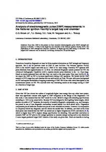
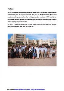
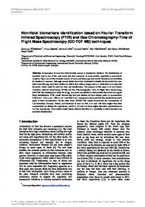
2 Bandstop DGS filter The configuration of dual band bandstop microstrip filter is illustrated in Figure 1. Figure 1 show the dual-band bandstop microstrip resonator filter without DGS. The ground plane is etched in rectangular pattern. The slot DGS pattern consists of length, l and width, w, as illustrated in Figure 2. Figure 3 shows the dual band bandstop filter with DGS. The configuration is designed by using R04003C printed circuit board with dielectric constant of 3.38 and a thickness of 0.508mm. The specifications of bandstop filter are shown in Table 1. Table 1. Bandstop filter specifications Physical Parameter Center Frequency, f0
Specifications 2.4 GHz and 5.8 GHz
Insertion loss, S21
≤ -10 dB
Return loss, S11
≥ -1 dB
*Corresponding author:
[email protected] © The Authors, published by EDP Sciences. This is an open access article distributed under the terms of the Creative Commons Attribution License 4.0 (http://creativecommons.org/licenses/by/4.0/).
EPJ Web of Conferences 162, 01063 (2017) InCAPE2017
DOI: 10.1051/epjconf/201716201063
Based on the orientation or configuration from Figure 1, the layout is combined both resonators in one single transmission line to obtain dual band bandstop filter. In obtaining an easy layout, miniature and compact size, [13] the layout is designed as illustrated in Figure 1. The slot defected ground structure (DGS) as shown in Figure 2 are added to the design layout in Figure 3. The insertion loss (S21) and return loss (S11) of the bandstop filter are improved the performances by using DGS [14].
5.8 GHz
Fig. 3. Dual band bandstop microstrip filter with DGS
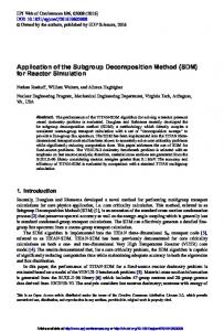
3 Results and Discussion Based on the structure in Figure 1, the simulation result shows in Figure 4. There are two center frequencies of bandstop filter. The first resonant frequency is at 2.40 GHz and the second resonant frequency delivers at 5.80 GHz. The insertion loss, S21 in the stop bands are -8.45 dB and -10.42 dB. The return loss, S11 shows at -3.23 dB and -3.11 dB on it.
2.4 GHz
Fig. 1. Dual band bandstop microstrip filter without DGS
w
l Fig. 4. Simulation result for dual band bandstop microstrip filter without DGS
However, the resonant frequency is affected and varied due to the improper length and width of the slot DGS in the ground structure. The center frequency are shifted when applied the slot DGS in the ground structure. From the studies, the DGS width is found slightly or less impact to the variation of the resonant frequencies. This is due to the lack of tightness of the current density in the DGS width direction [15]. However, the DGS length is significantly and gives a huge impact to the resonant frequencies. Moreover, the DGS length controlled the resonant frequency and the DGS width has little impact on it. Figure 4 and Figure 5 shows the simulation S-parameter results of DGS length and width. Initially, both DGS widths are set at 0.3 mm for both resonators and the DGS length are varying with
Fig. 2. Rectangular shaped DGS pattern
2
EPJ Web of Conferences 162, 01063 (2017) InCAPE2017
DOI: 10.1051/epjconf/201716201063
different length that are 5mm, 7mm and 10mm. Referring to Figure 4(a) and (b) shows the simulation result for insertion loss, S21 and return loss, S11 by using different length of DGS.
DGS widths are 0.3 mm, 0.6 mm, 0.9 mm and the DGS length is permanently set at 5 mm.
(a) (a)
(b)
(b)
Fig. 4. DGS with different length (a) Insertion loss, S21 (b) Return loss, S11
Fig. 5. DGS with different width (a) Insertion loss, S21 (b) Return loss, S11
The simulated results are tabulated in the Table 2. As a conclusion, from the simulated results as shown in Figure 4 and 5, the best width and length of the DGS are 0.3 mm and 5 mm. At these DGS dimension values, it delivers 2.32 GHz (S21 = - 12.31 dB) and 5.4 GHz (S21 = -22.93 dB) that are nearest results to the resonant frequency at 2.4 GHz and 5.8 GHz.
Analysing the simulated results in Figure 4, it is realized that if the length increased the center frequency decreased. Hence, the best DGS length for both resonators are 5 mm since it can deliver the nearest target resonant frequencies which at 2.32 GHz and 5.4 GHz. To improve the S-parameters and resonant frequencies, the proper DGS width is needed to be analysed. Figure 5 shows the effects of the DGS width on Sparameters and resonant frequencies. The simulated
3
EPJ Web of Conferences 162, 01063 (2017) InCAPE2017
DOI: 10.1051/epjconf/201716201063
Table 2. Result for varying dimension of length and width of DGS Resonance Frequency (GHz)
Length of DGS (mm)
Width of DGS (mm)
Insertion loss, S21(dB)
Return loss, S11 (dB)
f1 =2.4
f2 =5.8
f1 =2.4
f2 =5.8
f1 =2.4
f2 =5.8
5
2.32
5.40
-12.31
-22.93
-1.75
-0.78
7
2.24
5.00
-17.69
-25.00
-1.31
-0.43
10
2.14
4.48
-19.03
-29.94
-0.77
-0.34
0.3
2.32
5.40
-12.31
-22.93
-1.75
-0.78
0.6
2.30
5.30
-18.19
-23.00
-1.75
-0.69
0.9
2.28
5.20
-19.12
-24.86
-1.57
-0.60
The comparison results between dual band bandstop microstrip filter with and without DGS are shown as in Figure 6. From the Table 3,it is shows that the resonant frequencies slightly changes when the design are added with slot DGS. It is changes from 2.4 GHz to 2.32 GHz and 5.8 GHz to 5.4 GHz. It is due to the etched area in the ground plane that modify the characteristics of transmission line. It will produced the effective capacitance and inductance. The path of the ground current will increase when the etched area of DGS increase, hence increase the inductance. Thus, the capacitance will decreased since the distance between the ground and the signal line has increased. As the increasing the inductance, the resonance frequency will decrease to a lower cut off frequency. With the result that, it indicates that the etched area in the ground plane provides for impact of the cut off frequency whether it is shift up or down. Therefeore, to obtain the target frequencies (at 2.4GHz and 5.8 GHz) both resonator will be optimized by varying the dimensions of the width and length. However, the resonant frequency shifted, the Sparameters of insertion loss(S21) and return loss(S11) is improved to high performances. The slot DGS increase the slow wave factor that enhances the coupling between lines. As a results, it is shows that defected ground structure (DGS) can increase the rejection level of Sparameters performance.
Fig. 6. Comparison between dual band bandstop filter with and without DGS Table 3. Comparison results between dual band bandstop microstrip filter without and with DGS Without DGS
With DGS
Center Frequency
2.4 GHz 5.8 GHz
2.32 GHz 5.4 GHz
Insertion loss, S21
-8.45 dB -10.42 dB
-12.31 dB -22.93 dB
Return loss, S11
-3.23 dB -3.11 dB
-1.75 dB -0.78 dB
4 Conclusions In this paper, dual band bandstop microstrip filter are designed by applied the rectangular shaped defected ground structure (DGS). The dimension of width and
4
EPJ Web of Conferences 162, 01063 (2017) InCAPE2017
DOI: 10.1051/epjconf/201716201063
length of DGS is analyzed by varying with different parameters. By varying the parameter, it is tuning the resonant frequency and the S-parameters. Moreover, the comparisons between dual band bandstop microstrip filter with and without DGS are shown in this paper.
References 1. 2. 3.
4. 5. 6. 7. 8.
9. 10.
11. 12.
13.
14.
15.
D. Cui, Y. Liu, Y. Wu, S. Li, and C. Yu, Progress Electromagnetic Research, 121, pp. 271–279, (2011). Y. Luo and Q. Chu, European Microwave Conference, pp. 25–28, (2013). M. K. Zahari, B. H. Ahmad, N. A. Shairi, and P. W. Wong, IEEE Symposium Wireless Technology Applications ISWTA, pp. 71–74, (2012). W. Wang, M. Liao, Y. Wu, and Y. Liu, Electronics Let., 50, 4 pp. 286–288, (2014). H. Ning, J. Wang, Q. Xiong and L. Mao, Progress in Electromagn. Res., 131, pp. 259– 274, (2012). Y. Huang, S. Yang, L. Su, and C. C. Tzuang, Proceedings of APMC, pp. 235–237, (2012). J. Qiu, F. Chen, and Q. Chu, IEEE Int. Wireless Conf., pp. 9–11, (2013). S. U. Rehman, A. F. Sheta, and M. Alkanhal, IEEE SIECPC-Saudi International Electronics, Communications and Photonics Conference, Riyadh, Saudi Arabia, 1,( 2011). L. H. Weng, Y. C. Guo, X. W. Shi, and X. Q. Chen, Progress in Electromagnetic Research B, 7, pp. 173–189, (2008). A. Rahman, A. Boutejdar, A. K. Verma, G. Nadim, and A. S. Omar, Antennas and Propagation Society International Symposium, 2004. IEEE 1, pp.998-1001, (2004). B. G. Breed, High Frequency Electronics, November, pp. 50-54,(2008). P. Singh, R. Tomar and P. Bhartia, “International Journal of Advanced Research in Computer and Communication Engineering, 2, 10, pp. 3942–3948, (2013). S. Saxena, S. Porwal, K. Soni, P. Chhawchharia, and S. K. Koul, IEEE International Conference. Microwaves, Communications, Antennas and Electronics Systems, COMCAS, (2009). S. U. Rehman, A. F. a. Sheta, M. a. S. Alkanhal, and R. S. Aziz, Saudi International Electronisc, Communications and Photonics Conference, 1, pp. 1–4, (2013). N. C. Karmakar, S. Member, S. M. Roy, and I. Balbin, IEEE Transactions on Microwave Theory and Techniques, 54, 5, pp. 2160–2168, (2006).
5