International Journal of ChemTech Research CODEN (USA): IJCRGG ISSN : 0974-4290 Vol.6, No.5, pp 3220-3227, Aug-Sept 2014
Effect of Deposition Time on Structural and Optical Properties of ZnS Nanoparticles Thin Films Prepared by CBD Method Raghad Zein, Ibrahim Alghoraibi*, Damascus University, Physics Department, Baramkeh- Damascus, SYRIA
*Corres. author:
[email protected] Phone: +963-99-26-78-26-8, Fax: +963-11-21-19-89-6
Abstract: In this paper, we report the effect of deposition time on the properties of zinc sulfide thin films. The ZnS thin films have been grown on amorphous glass substrates and at various deposition periods ranging from 30 to 120 min by chemical bath deposition technique. The other parameters: concentration of the reactants, pH of solution, and temperature of bath were kept constant for the all depositions. Morphological characterizations of the surface were studied using the atomic force microscopy, The AFM images confirmed that the grain size of ZnS increased with increasing of deposition time. Average diameter of nanoparticles were between 152 and 202 nm while roughness ranged from 6 to 11 nm. UV-VIS spectrophotometer were used to obtain optical properties which determined from analysis of measured absorbance, transmittance spectrum. The zinc sulfide thin films show high transmittance in the visible region and the ZnS band gap value was estimated to be in range of 3.99- 4.05 eV. Key Words: Zinc sulfide NanoParticles (ZnS-NPs), Chemical Bath Deposition (CBD), Atomic Force Microscopy (AFM).
1. Introduction Zinc sulfide (ZnS) is a wide direct band gap, high optical absorption coefficient, reasonable work function. It has attracted considerable attention due to its excellent electrical and optical properties with its distinct properties has become the potential candidate for many applications 1 such as, electroluminescence devices, photonic device, field emission devices2,3, and nontoxicity it considers an ideal project for fabrication of high-performance sensors4,5 and important for applications in infrared windows6 and lasers7,8. High band gap of ZnS-NPs (3.5–3.8 eV) should improve the solar cell device efficiency by eliminating absorption loss in the short wavelength region8. Several methods have been applied to prepare ZnS thin film such as thermal evaporation10, sputtering11, spray pyrolysis12, chemical vapor deposition(CVD) 13, molecular beam Epitaxy (MBE)14, pulsed laser deposition (PLD)15, microwave16,17, sol-gel processes18, sonochemical preparation19, Green synthesis20. Among various other methods the chemical bath deposition CBD that we use in present case is a well known deposition process for some chalcogenides such as Zn, Co, Cd, Hg, Pb, sulphides and selenides, it is well known as prevented low temperature aqueous technique for deposition large area of semiconductor thin films and has gained renewed interest due to the good quality and high purity of the deposited films. CBD of ZnS is a highly reproducible and controllable technique, so it considered the simplest and the most economical one. CBD results good deposits on suitable substrates by controlled precipitation of the compound from the solution.
Ibrahim Alghoraibi et al /Int.J. ChemTech Res.2014,6(5),pp 3220-3227.
3221
In the present work, we report the chemical bath deposition of ZnS thin films and their characterization. The effect of deposition time on morphological and optical properties of ZnS thin films, by using atomic force microscopy and UV-VIS spectrometry respectively, is investigated with the objective to optimize the conditions of the deposition process.
2. Experimental materials and methods: 2-1.
Reaction mechanism :
The basic principle of the CBD technique consists in the controlled generation of the metal and chalcogenide ions in an alkaline medium and their ion by ion deposition on the substrate in order to form a film. In our CBD experiment, the deposition of ZnS film was based on the reaction between zinc sulfate (ZnSO4 ) as a source of Zn2+, Thiourea (SC(NH2)2) as a source of S 2- and ammonia (NH4OH) that used as complexing agent to vary the pH of the reaction bath and to control the Zn2+ concentration. The chemical process can be described through the following chemical reactions: Zn2+ + 2OH- → Zn(OH)2 NH4+ + OH- → NH3 + H2O Zn(OH)2 + 4NH3→ [Zn(NH3)4]2+ + 2OHCS(NH2)2 + 2OH- → S2- + CN2H2 + 2H2O Finally the ZnS films are formed on glass substrates that is immersed in reaction solution according to the relation: [Zn(NH3)4]2+ + S2-→ ZnS(s) + 4NH3 2-2.
Deposition of ZnS films :
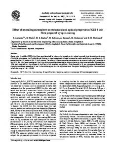
ZnS films were deposited on commercial glass substrates (75mm × 25mm × 1mm) by chemical bath deposition technique. Prior to deposition, the substrate was degreased in ethanol for 10 min, followed by ultrasonically cleaned with double distilled water for another 10 min, rinsed in de-ionized water and finally dried in the air. In a typical deposition set up of ZnS, the CBD was achieved by mixing 10 ml of 0.025M ZnSO4 solution,10 ml of 0.27M SC(NH2)2 solution, and 2.9 M NH4OH solution. Firstly, ammonia solution was added slowly to the required quantity of zinc sulfate, after stirring for several minutes the solution becomes colorless and homogeneous, there after thiourea solution was added under stirring. Lastly, the reaction solution was placed in 50 ml beaker (sealed with a Teflon tape) into the water bath pot The glass substrates were then immersed vertically inside this beaker and supported against the wall of the beaker without disturbing it. Fig. 1 shows an experimental setup for chemical bath deposition technique.
Fig. 1: Experimental setup for chemical bath deposition of thin film.
3222
Ibrahim Alghoraibi et al /Int.J. ChemTech Res.2014,6(5),pp 3220-3227.
The deposited film was carried out water bath temperature at Tb=70°C, for different durations, (30, 60, 90, 120 min) that were selected to study the characteristics of ZnS thin films. After completion of film deposition, each sample was removed from the beaker and was cleaned with de-ionized water to remove the white, loosely, adherent powders precipitate in the solution during the deposition. The atomic force microscopy (AFM) was used to investigate the surface morphology and surface roughness. AFM imaging is performed on the Nanosurf system (easyScan2) operating in a tapping mode in air at room temperature. The optical transmission and absorption studies of the deposited ZnS thin films were carried out with a UV-VIS spectrophotometer (Varian carry 5000).
3
Results and discussion:
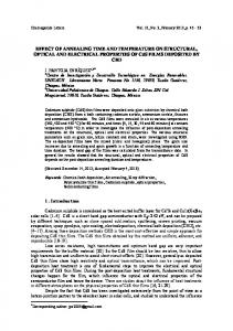
3.1 Morphological properties: AFM allows us to get microscopic information on the surface structure and to plot topographies representing the surface relief. In this work, we have used this technique to visualize the surface relief, specify the growth, and determine the contribution of the time deposition (td) to the quality of the film. AFM images of the surface morphology recorded on samples of the ZnS-NPs thin films deposited with different deposition time periods for (td=30, 60, 90, 120 min) are shown in Fig. 2.
30 90 min
120 min 60 min
d b
ca 2 μm
2 μm
Fig. 2: 10x10μm AFM images for ZnS thin films/glass at different deposition time : a) td =30min, b) td =60min, c) td =90min, d) td =120min. In all cases the prepared thin films have good quality, uniform morphology and covered the entire substrate surface. In Fig. 2(a, b) at lower deposition time (30, 60 min) the ZnS-NPs carpet the substrate with uniformly spherical shape and have relatively low and narrow size distributions. In the case of ZnS layers grown at 90 min Fig. 2(c) the grain size increase and the particles start to aggregate and made clusters, more clusters showed in Fig. 2(d) for 120 min. We can expect this result due to the increase of the film thickness with the deposition time.
3223
Ibrahim Alghoraibi et al /Int.J. ChemTech Res.2014,6(5),pp 3220-3227.
Fig. 3 shows the mean grain diameter of ZnS-NPs in function of deposition time, it was between 152202 nm, it appears that the particle size increased with increasing of the deposition time. The same relation between the mean height of ZnS-NPs and the deposition time has been observed.
200
Mean Diameter (nm)
180
160
140 30
60
90
120
60
90
120
90
120
30
Mean Height (nm)
25
20
15 30 12
Mean Square Roughness
10
8
6
30
60
Deposition Time (nm)
Fig.3 : Changes of mean diameter (triangle symbols), mean height (circle symbols) and mean square roughness (square symbols) of ZnS thin film versus deposition time. The mean surface roughness determined from AFM images for deposition time 30, 60, 90,120 min were found to be 6, 9, 10, and 11 nm, respectively. As it can be seen the increasing of roughness by increasing deposition time and that because of formation of new bigger domed grains form and the layer get more completed and fraction of voids decreases. It is important to note that these obtained values are averaged and there is a statistical variation associated with them which depends on the location of the measurement that is performed on the samples21. To minimize these errors, we have performed many measurements of each parameter in different locations on the surface of samples.
Ibrahim Alghoraibi et al /Int.J. ChemTech Res.2014,6(5),pp 3220-3227.
3224
3.2 Optical properties The evolution of the optical properties of the prepared ZnS thin films were determined after obtaining the absorbance and transmittance spectrum. UV-Vis transmittance spectra of ZnS-NPs formed at bath or reaction temperature of 70 ºC with different reaction times (30, 60, 90, 120 min) are given in Fig. 4. It was recorded over the wavelength range 300- 800 nm. The transmission of the thin films of zinc sulfide decreases with the increase in deposition times. The average transmittance of these films is calculated to be 99%, 97.5%, 96%, and 95%, respectively. This result related to the increasing of deposition time so the voids in ZnS thin layer fill up with new ZnS grains and that tends to more thickness and less transmittance. In general there are high percent of transmittance for layers produced in this work, that depends on low thickness of thin film. In addition to the decreasing of transmittance can be linked with the agglomeration and increasing in the grain size, and indicating its high surface roughness.
Fig. 4: Transmittance spectra of ZnS thin film at different deposition times (30,60,90,120 min)
The thickness of the prepared films was measured by optical interference fringes method, it was 73, 80, 86 and 91 nm. for 30,60, 90, 120 min deposition times respectively. The ZnS thin films have a steep optical absorption feature, indicating good homogeneity in the shape and size of the ZnS-NPs and low defect density. To obtain the absorption characteristics of all the samples. At first, transmittance (T) at different wavelengths (λ) are measured and then absorption coefficient (α) at the corresponding wavelengths are calculated by using the following equation:
Where (T) is the transmittance and (t) is the thickness of the thin films. Fig. 5 shows the absorption coefficient a as function of the photon energy; a decreases in the law photon energy the probability of the electrical transfer between valance band and the conduction band is very rare and it will increase in the edge of the absorbance toward the high energy. Using last data, the band gap energy of ZnS thin film was estimated by plotting against as in Fig. 6, the linear nature of the plot indicates that ZnS is a direct band gap material. The optical band gap of the films can evaluate from extrapolating the straight portion to the axis.
3225
Ibrahim Alghoraibi et al /Int.J. ChemTech Res.2014,6(5),pp 3220-3227.
5
3.0x10
30 min 60 min 90 min 120 min
5
-1
absorption cofficient a (cm )
2.5x10
5
2.0x10
5
1.5x10
5
1.0x10
4
5.0x10
0.0 4
-5.0x10
5
-1.0x10
3.6
3.8
4.0
4.2
4.4
photon energy (eV)
Fig. 5: Absorption coefficient versus photon energy for ZnS thin films deposited at different times (30,60,90,120 min) In this work the band gap energy (Eg) was determined to be in the range of 4.05-3.99 eV for the ZnS films with deposited at different times from 30 to 120 min, respectively which closely agree with the values reported for ZnS thin films obtained by CBD22,23. The band gap values of the as deposited ZnS films are somewhat larger than the typical band gap of bulk ZnS (~3.6 eV) at 300 K. In Fig. 7, we have reported the variation of band gap energy and thickness of thin film ZnS –NPs as a function of deposition time. We note a reduction in the gap with the deposition time this due to the quantum size effect as expected for the nanoparticles nature of the films24.
0.10
0.10
t= 30 min 0.08
t= 60 min
2
2
(ahn) /(10 cm eV )
(ahn) /(10 cm eV )
0.08
0.06
13
13
2
2
0.06
0.04
2
2
0.04
0.02
0.02
0.00
0.00 1.0
1.5
2.0
2.5
3.0
3.5
4.0
1.0
1.5
Photon energy hn (eV)
3.0
3.5
4.0
3.5
4.0
0.10
t= 120 min
t= 90 min
0.08
2
(ahn) /(10 cm eV )
0.08
0.06
2
0.06
13
13
2
2
2.5
photon energy hn(eV)
0.10
(ahn) /(10 cm eV )
2.0
0.04
2
2
0.04
0.02
0.02
0.00
0.00 1.0
1.5
2.0
2.5
3.0
photon energy hn(eV)
Fig. 6: The plot of
3.5
4.0
1.0
1.5
2.0
2.5
3.0
photon energy hn(eV)
versus of ZnS nanoparticles deposited at different times (30, 60, 90, 120 min).
3226
Ibrahim Alghoraibi et al /Int.J. ChemTech Res.2014,6(5),pp 3220-3227.
Band gap energy (eV)
Film thickness (nm)
In fact, it is observed that the band gap energy values of ZnS thin layers decrease lightly from 4.05 to 3.99 eV with increasing deposition time. There was a good agreement between structural and optical properties and calculated band energy gap. The thickness of ZnS thin film slightly increases from 73 nm to 91 nm when the deposition time increases respectively from 30 to 120 min, this may be due to the process of heterogeneous and homogenous precipitations which increase with time leading to more growth rate of ZnS thin films.
96 90 84 78 72 4.06
30
60
90
120
4.04 4.02 4.00 3.98 30
60
90
120
Deposition time (min)
Fig. 7: Variation of ZnS thin films thickness and band gap with deposition times at fixed bath temperature Tb=70 ºC
4
Conclusion:
We have successfully used chemical bath deposition to obtain ZnS/glass thin films. AFM showed that the films were of good quality and have uniform distribution of ZnS-NPs over the glass substrate. Images revealed that the particle size increased with increasing of deposition time, the average diameter was 180 nm. High transparency of the films, over 95%, was investigated using UV VIS spectrophotometer. The optical direct band gap energy are calculated to be between 3.99 4.05 eV for the ZnS films with different thicknesses. Structural and optical properties were in agreement with each other. From these studies we are able to optimize the process in order to produce the antireflection layer of ZnS suitable for optical window in solar cells.
References 1. 2. 3. 4. 5. 6.
Xiaosheng F., Tianyou Z., Ujjal K., Gautam., Liang Li., Limin Wu., Yoshio B., and Dmitri Golberg , "ZnS nanostructures : From synthesis to applications". Progress in Materials Science 56 (2011) 175– 287 Fang XS, Bando Y, Shen GZ, Ye CH, Gautam UK, Costa PMFJ, et al. Ultrarine ZnS nanobelts as field emitters. Adv Mater. 2007;19:2593. Fang XS, Gautam UK, Bando Y, Dierre B, Sekiguchi T, Golberg D. Multiangular branched ZnS nanostructures with needle-shaped tips: Potential luminescent and field-emitter nanomaterial. J PhysChem C. 2008;112:4735-42. Fang XS, Bando Y, Liao MY, Gautam UK, Zhi CY, Dierre B, et al. Single-Crystalline ZnS Nanobelts as Ultraviolet-Light Sensors. Adv Mater. 2009;21:2034-9. Uematsu T, Taniguchi S, Torimoto T, Kuwabata S. Emission quench of water-soluble ZnS-AgInS(2) solid solution nanocrystals and its application to chemosensors. Chem Commun. 2009:7485-7. Pratap S, Prasad J, Kumar R, Murari K, Singh SS. Preparation &characterisation of IR window grade zinc sulphide powder. DefenceSci J. 1996;46:215-21.
Ibrahim Alghoraibi et al /Int.J. ChemTech Res.2014,6(5),pp 3220-3227.
7. 8. 9. 10. 11. 12. 13. 14. 15. 16.. 17. 18. 19. 20. 21. 22. 23. 24.
3227
Page RH, Schaffers KI, DeLoach LD, Wilke GD, Patel FD, Tassano JB, et al. Cr2+-doped zinc chalcogenides as efficient, widely tunable mid-infrared lasers. Ieee J Quantum Elect. 1997;33:609-19. Fang XS, Bando Y, Gautam UK, Zhai TY, Zeng HB, Xu XJ, et al. ZnO and ZnS Nanostructures: Ultraviolet-Light Emitters, Lasers, and Sensors. Crit Rev Solid State. 2009;34:190-223. Bhattacharya RN, Ramanathan K. Cu(In,Ga)Se-2 thin film solar cells with buffer layer alternative to CdS. Sol Energy. 2004;77:679-83. V. Dimitrova, J. Tate, Thin Solid Films 365 (2000) 134. L.-Z. Shao, K.-H. Chang, H.-L. Hwang, Appl. Surf. Sci. 212–213 (2003)305. A.N. Yazici, M. Oztas, M. Bedır, J. Lumin. 104 (2003) 115. D. Barreca,A. Gasparotto, C. Maragno,E. Tondello and C. Sada, Chem. Vapour Depos. 10 (2004) 229. Y. Kavanagh and D.C. Cameron // Thin SolidFilms 398-399 (2001) 24. S. Yano, R. Schroeder, B. Ullrich and H. Sakai// Thin Solid Films 423 (2003) 273. Soltani, N.; Saion, E.; Hussein, M.Z.; Bahrami, A.; Naghavi, K.; Yunus, R.B. Microwave irradiation effects on hydrothermal and polyol synthesis of ZnS nanoparticles. Chalcogenide Lett. 2012, 9, 265– 274. Robina Shahid, Mikhail Gorlov, Ramy El-Sayed, Muhammet S. Toprak, Abhilash Sugunan,Lars Kloo, Mamoun Muhammed. “Microwave assisted synthesis of ZnS quantum dots using ionic liquids” Materials Letters, 89 2012 316–319. Mohammad Syuhaimi Ab-Rahman, Noor Azie Azura Mohd Arif and Sahbudin Shaari " Effect of Thermal Treatment on the Morphology of ZnS:Mn Nanocrystals" World Applied Sciences Journal 12 (9): 1505-1511, 2011. Lee, S.S.; Byun, K.-T.; Park, J.P.; Kim, S.K.; Lee, J.C.; Chang, S.-K.; Kwak, H.-Y.; Shim, I.-W. Homogeneous ZnS coating onto TiO2 nanoparticles by a simple one pot sonochemical method. Chem. Eng. J. 2008, 139, 194–197. Senapati U.S., Jha D.K. and Sarkar. D, "Green Synthesis and Characterization of ZnS nanoparticles", Research Journal of Physical Sciences, Vol. 1(7), (2013) 1-6. M.A.Martynez,C.Guillen and J.Herrero // Appl.Surf.Sci. 140(1999)182. Haleh Kangarlou, Ladan Naseri, Tavakkol Tohidi, "An Investigation about Nano Structures of Zinc Sulfide Thin Layers Produced by Chemical bath deposition (CBD) Method", J. Basic. Appl. Sci. Res., 2(5)4807-4811, (2012). G. Nabiyouni, R. Sahraei, M. Toghiany, M. H. Majles Ara and K. Hedayati, "preparation and characterization of Nano-structures ZnS thin film grown on glass and n-type Si structures using a new chemical bath deposition technique" Rev, Adv, Mater, Sci. 27 (2011) 52-57. A. K. Kole P. Kumbhakar "Effect of manganese doping on the photoluminescence characteristics of chemically synthesized zinc sulfide nanoparticles", Appl Nanosci) 2:15–23(2012).
*****