Feb 5, 2015 - ... of ohmic contacts. arXiv:1502.01757v1 [cond-mat.mes-hall] 5 Feb 2015 ... ¯nmc . (3). It can be shown33 that, in the hydrodynamic ÏÏee ⪠1 limit, ν â v2 ... ports collective charge density oscillations, i.e. plas- mons3, which ...
Electrical plasmon detection in graphene waveguides Iacopo Torre,1 Andrea Tomadin,1 Roman Krahne,2 Vittorio Pellegrini,3, 1 and Marco Polini1, 3, ∗
arXiv:1502.01757v1 [cond-mat.mes-hall] 5 Feb 2015
2
1 NEST, Istituto Nanoscienze-CNR and Scuola Normale Superiore, I-56126 Pisa, Italy Istituto Italiano di Tecnologia, Graphene Labs and Nanochemistry Department, Via Morego 30, I-16163 Genova, Italy 3 Istituto Italiano di Tecnologia, Graphene Labs, Via Morego 30, I-16163 Genova, Italy
We present a simple device architecture that allows all-electrical detection of plasmons in a graphene waveguide. The key principle of our electrical plasmon detection scheme is the nonlinear nature of the hydrodynamic equations of motion that describe transport in graphene at room temperature and in a wide range of carrier densities. These non-linearities yield a dc voltage in response to the oscillating field of a propagating plasmon. For illustrative purposes, we calculate the dc voltage arising from the propagation of the lowest-energy modes in a fully analytical fashion. Our device architecture for all-electrical plasmon detection paves the way for the integration of graphene plasmonic waveguides in electronic circuits.
Introduction.—The two-dimensional (2D) electron liquid in a doped graphene sheet1 supports plasmons with energies from the far-infrared to the visible, depending on carrier concentration2 . Although they share similarities with plasmons in ordinary parabolic-band 2D electron liquids3 , plasmons in graphene are profoundly different. From a fundamental point of view, their dispersion relation is sensitive to many-body effects even in the long-wavelength limit4 . More practically, plasmons in graphene are easily accessible to surface-science probes and opto-electrical manipulation since they are exposed and not buried in a quantum well. Plasmons in graphene are also substantially different from those in noble metals. Indeed, recent near-field optical spectroscopy experiments5–9 have demonstrated that plasmons in graphene display gate tunability and ultrastrong field confinement. Moreover, low damping rates can be achieved by employing graphene samples encapsulated in hexagonal boron nitride thin slabs9–12 . For these reasons, graphene plasmonics has recently attracted a great deal of interest13 . Graphene plasmons may allow for new classes of devices for single-plasmon nonlinearities14 , extraordinarily strong light-matter interactions15 , deep sub-wavelength metamaterials16–19 , and photodetectors with enhanced sensitivity20,21 . A key ingredient of a disruptive plasmonic platform is the ability to efficiently detect plasmons in all-electrical manners. Some progress has been made in this direction in conventional noble-metal-based plasmonics. Falk et al.22 , for example, were able to couple plasmons in Ag nanowires to nanowire Ge field-effect transistors. Built-in electric fields in the latter are used to separate electrons and holes before recombination, thereby giving rise to a measurable source-drain current. Similarly, Neutens et al.23 employed an integrated metal-semiconductor-metal detector in a metal-insulator-metal plasmon waveguide. While graphene plasmons have been detected and studied in a multitude of ways13 , including electron energy loss spectroscopy24 , polarized Fourier transform
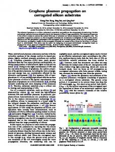
FIG. 1. (Color online) Schematics of our electrical plasmon detector. A graphene strip of width W is encapsulated between two dielectrics (semi-transparent slab above and dark green slab underneath graphene). A back gate (dark blue slab), separated by a distance d from the graphene sheet and held at a voltage VG , is used to control the average carrier density n ¯ in graphene. At one end of the strip, a plasmon is launched by using e.g a metallized atomic force microscope tip illuminated by light5–9 . Due to non-linearities in the hydrodynamic equations, a dc electrical potential difference δV is measured between probe electrodes placed at positions r1 , r2 , and r3 and a reference electrode placed at the other end of the strip. The quantity δV provides a direct measurement of the ac electric field of a propagating plasmon.
infrared spectroscopy16 , and near-field optical spectroscopy5–9 , a protocol for all-electrical detection of these modes is still lacking. In this work we present a device architecture that allows all-electrical detection of plasmons in graphene waveguides. In our scheme, all-electrical detection is not enabled by the integration of a detector in a graphene plasmon waveguide (GPW) but rather by the intrinsic non-linear terms in the hydrodynamic equations that describe transport in the 2D massless Dirac fermion (MDF) liquid1 hosted by graphene. Non-linearities enable the emergence of a rectified (i.e. dc) component δV (r) of the ac electric field of a propagating plasmon, which can be measured by a suitable geometry of ohmic contacts
2
placed along the GPW, as shown in Fig. 1. We now present a calculation of the spatially-dependent electrical signal δV (r). Hydrodynamic theory.—We consider a GPW with transverse (longitudinal) size W (L with L � W ), which is embedded between two insulators with dielectric constants �1 (above the GPW) and �2 (below the GPW). Here, “longitudinal” and “transverse” refer to the plasˆ in Fig. 1. mon propagation direction—x We would like to describe ac transport in a GPW by employing the theory of hydrodynamics25 . We therefore need to assess whether experimentally relevant regions of parameter space exist in which this theory is applicable. First, at room temperature and for typical carrier densities (¯ n ' 1011 cm−2 -5 × 1012 cm−2 ), the mean-free-path `ee = vF τee for electron-electron collisions in graphene is short26,27 , i.e. `ee ' 100-150 nm. Here, vF ' 106 m/s is the graphene Fermi velocity28 and τee ' 100 fs = 10−13 s is the electron-electron collision time26,27 . Second, for hydrodynamics to provide a correct description of the response of the system at finite frequencies, it must also be ωτee � 1, where ω is the external-excitation angular frequency. The value of τee given above constraints the maximum external-excitation frequency to be fmax ≡ 1/(2πτee ) . 3 THz. We therefore conclude that, for n ¯ ' 1011 cm−2 -5 × 1012 cm−2 , ω < 2πfmax , and T = 300 K, transport in GPWs with characteristic dimensions L, W � `ee is accurately described by hydrodynamic equations of motion25 . Related continuum-model descriptions of plasmons in GPWs have been employed in Refs. 29–32. The set of hydrodynamic equations consists of i) the continuity equation, ∂t n(r, t) + ∇ · [n(r, t)v(r, t)] = 0 ,
(1)
and ii) the Navier-Stokes equation25 mc n(r, t)Dt v(r, t) = −en(r, t)E(r, t)+η∇2 v(r, t) . (2) In Eqs. (1)-(2), n(r, t) is the carrier density √ and v(r, t) is the drift velocity. In Eq. (2), mc = ~ π¯ n/vF is the graphene cyclotron mass28 , with n ¯ = CVG /e the average electron density and VG the back-gate voltage (see Fig. 1), and Dt ≡ ∂t + v(r, t) · ∇ is the convective derivative25 . The electric field E(r, t) = −∇Φ(r, t) is the gradient of the electrostatic potential Φ(r, t) (we neglect retardation effects). Finally, η is the shear viscosity of the 2D electron liquid3,25 . For future purposes, we also introduce the kinematic viscosity25 ν≡
η . n ¯ mc
(3)
It can be shown33 that, in the hydrodynamic ωτee � 1 limit, ν ' vF2 τee /4. With the values of vF and τee given above, we find ν ' 250 cm2 /s. In writing Eq. (2) we have neglected a term due to the bulk viscosity ζ since this quantity vanishes at long wavelengths3,25 .
We highlight two non-linear terms in Eqs. (1)-(2): a) the non-linear coupling between n(r, t) and v(r, t), which is present in Eq. (1), and b) the non-linear term [v(r, t) · ∇]v(r, t) in Eq. (2), representing the convective acceleration25 . Momentum-non-conserving collisions, such as those due to the friction of the electron liquid against the disorder potential, can be taken into account phenomenologically by adding a term of the type −mc γn(r, t)v(r, t) on the right-hand side of Eq. (2), where γ is a damping rate34 . Furthermore, corrections to Eq. (2), stemming from the pseudo-relativistic nature of MDF flow in graphene, can be easily incorporated into the theory35,36 and have been demonstrated to yield stronger rectified signals35 . Finally, to close the set of equations, we need a relation between Φ(r, t) and n(r, t). This depends on the screening exerted by dielectrics and conductors near the GPW. If a metal gate is positioned underneath the GPW at a distance d � W, k −1 , where k is the plasmon wave vector, the following local relation exists35 : Φ(r, t) ≈ −
e δn(r, t) , C
(4)
where C = �2 /(4πd) is a capacitance per unit area and δn(r, t) ≡ n(r, t) − n ¯ . Eq. (4) greatly simplifies the theoretical analysis and, in fact, allows us to solve the problem in a fully analytical fashion37 , as we now detail. Eqs. (1)-(4) need to be accompanied by boundary conditions. As explained in Appendix A and in Ref. 38, we fix vy (x, y = 0, W ) = 0 and ∂x vy (x, y = 0, W ) + ∂y vx (x, y = 0, W ) = 0. Linear response theory and plasmons.—The GPW supports collective charge density oscillations, i.e. plasˆ direction and are mons3 , which propagate along the x confined in the yˆ direction. To calculate the frequency spectrum and potential profiles of these modes we have to linearize Eqs. (1)-(2) and (4). We write n(r, t) = n ¯+ n1 (r, t) + n2 (r, t) + . . . , v(r, t) = v1 (r, t) + v2 (r, t) + . . . , and Φ(r, t) = Φ1 (r, t) + Φ2 (r, t) . . . . Here n1 (r, t), v1 (r, t), and Φ1 (r, t) [n2 (r, t), v2 (r, t), and Φ2 (r, t)] denote first-order [second-order] corrections with respect to equilibrium values (by “equilibrium” we here mean the state of the GPW in which a plasmon is not propagating). In the linearized theory we retain only terms of the first order. All the relevant details are reported in Appendix B and C. For the sake of simplicity, we assume a uniform equilibrium electron density in the GPW, disregarding the well known inhomogeneous doping n ¯→n ¯ (y) that arises due to a back gate. Plasmons in back-gated waveguides, however, have been demonstrated39 to be similar to those of uniformly doped waveguides, provided that the Fermi energy is appropriately scaled to compensate for the singular behavior of the carrier density n ¯ (y) as y → 0, W . Plasmon modes are labelled by a wave number k (stemˆ direction) ming from translational invariance along the x and a discrete index n = 0, 1, 2, . . . . The associated ac
3
electrical potential is given by (5)
f [THz]
Φ1 (r, t) = ϕn (y)eikx−iωn (k)t , where 1, for n = 0 √ . 2 cos[nπy/W ], for n 6= 0
(6)
The mode dispersion reads as following r (γ + νKn2 )2 γ + νKn2 ωn (k) = s2 Kn2 − −i , (7) 4 2 p ¯ /(Cmc ) where Kn2 = k 2 + qn2 , qn ≡ πn/W , and s = e2 n is the hydrodynamic speed of sound. It is useful to introduce the following natural frequency scale: Ω0 ≡ s/W . Setting external (γ) and internal (ν) dissipation to zero in Eq. (7) we find the expected result ωn (k) = sKn . The lowest-energy n = 0 mode shows an acoustic dispersion due to screening by the back gate. Modes with n 6= 0 are gapped, i.e. ωn (k → 0) = nπΩ0 . The fundamental frequency is ωn=1 /(2π) = Ω0 /2 ' 1.0 THz for W = 3 µm, d = 100 nm, �2 = 3.9, and n ¯ = 1012 cm−2 . Dispersion relations and mode profiles for the above set of parameters are shown in Fig. 2. In the approximation (4) the results do not depend on �1 . When the n-th eigenmode of the GPW is excited by an external perturbation with frequency ω, it propagates with a complex wave number r ω 2 + iωγ kn (ω) = − qn2 . (8) s2 − iνω The wave number,