Electronic transport properties of ternary Cd1-xZnxS nanowire network 1
Daeha Joung1,2, M. Arif1, S. Biswas1, S. Kar1, S. Santra1,3,4 and Saiful I. Khondaker 1,2*
Nanoscience Technology Center, 2Department of Physics, 3Department of Chemistry and 4 Biomolecular Science Center, University of Central Florida, 12424 Research Parkway, Suite 400, Orlando, FL 32826 * To whom correspondence should be addressed. E-mail:
[email protected] Abstract We present electronic transport characteristics of ternary alloy Cd1-xZnxS nanowire networks in the dark and under white light illumination. Compared to the negligible dark current, we observed a photocurrent enhancement up to 4 orders of magnitude at intensity of 460 mW/cm2. The time constant of the dynamic photoresponse is ~5 sec. The current – voltage characteristics at different intensities show Ohmic behavior at low bias and space charge limited conduction (SCLC) at higher bias voltages. The SCLC behavior and slow time response indicate that the charge transport is dominated by tunneling at the percolating inter-nanowire junctions.
(Some figures in this article are in color only in the electronic version) 1. Introduction: Chemically synthesized semiconductor nanocrystals have attracted tremendous interest because of the ability to tune their band gap through variation of their sizes and shapes. These nanocrystalline materials, specially that work in the visible range, have great potential for applications in optoelectronic devices such as solar cells, light emitting diodes, lasers, waveguides and photodetectors [1-5]. In addition, their ease of processibility from solution is of great advantage as they can cover large areas at low cost and are compatible with flexible substrates. Many studies have been done on semiconductor quantum dots [4-8] and quantum dot polymer composites [9-11]. However, it is believed that materials that are one dimensional (nanorods, nanowires) can provide added benefit as they make a percolating pathway for charge transport rather easily compared to zero dimensional quantum dots. There have been several reports on the optoelectronic studies of binary nanowires (NWs) [1-3, 12-15]. For example, Huynh et al used CdSe nanorods for making organic-inorganic hybrid solar cells [2]. Kind et al used ZnO NWs for ultraviolet photodetectors and optical switches [3]. Nonetheless, tuning the bandgap by varying the diameter and aspect ratio of one-dimensional NWs is extremely challenging. An alternative route of tuning the bandgaps of NWs is to engineer the relative composition of the materials to fabricate ternary alloy NWs. Despite the obvious advantage of ternary nanowires over binary NWs, there are only a few reports on the growth and optical properties of several ternary NW systems [16-19], and no reports on the optoelectronic investigation of any ternary NWs. Study of charge transport and photoresponse properties of ternary NW network film is important in order to determine whether this material could be useful for optoelectronic applications. In this paper, we report on the first optoelectronic transport characteristics of ternary alloy Cd1-xZnxS NW network devices. The NW films were prepared by drop-casting the NWs from solution on inter-digitated gold source and drain electrodes fabricated on Si/SiO2 substrate.
1
The current – voltage (I – V) characteristics were measured in the dark and under illumination from white light of different intensity using a xenon lamp (oriel solar simulator). The dark current was negligible, while the current under illumination increases almost linearly upon increasing the intensity of the light. We observed an enhancement of photocurrent up to four orders of magnitude compared to the dark current at an intensity of 460 mW/cm2 and a bias voltage of 15 V. The time constant of dynamic photoresponse is slow (~ 5 sec). The I-V curve at different intensities show Ohmic behavior at low bias and space charge limited conduction (SCLC) at high bias voltage. The space charge limited conduction along with slow time response show that the charge conduction is dominated by the carrier tunneling through inter-NW junctions. This study will have significant impact on the use of Cd1-xZnxS NWs in optoelectronics. 2. Experimental details:
Absorbance (arb. unit)
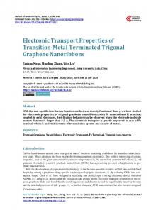
The Cd1-xZnxS NWs were grown following our recently developed technique [20]. Briefly an appropriate amount of zinc acetate [(CH3COO)2Zn, 2H2O], cadmium acetate [(CH3COO)2Cd, 4H2O], and thiourea (tu, NH2CSNH2) were placed in the Teflon-lined chamber, which was then filled with an ethylenediamine (en, NH2CH2CH2NH2) (a) and water mixture with 2:1 volume ratio up to 80% of its volume. The closed chamber was placed inside a pre-heated oven at 175 °C for 8 hours and then cooled at room temperature. The resulting precipitates were filtered off and rinsed several times in water and ethanol, then (b) dried in vacuum at room temperature for 6 hours to obtain the final powder product. Figure 1(a) shows the representative transmission electron microscopy image of CdS Cd1-xZnxS NWs with x=0.75. The NW is Cd Zn S single crystalline and the average diameter Cd Zn S of the NWs is between 8 to 15 nm which 350 400 450 500 550 600 remains almost the same with the variation Wavelength (nm) in the composition of alloy NWs, while (c) the length of the NWs can be up to 500 nm hν [20]. In this paper we used three different NW samples with x = 0, 0.25, 0.75. The band gap energy of the NWs increases from 2.37 eV to 3.13 eV for the increase in VSD W the x value from 0 to 0.75 as revealed I from the UV-vis absorption spectra in Figure 1. (a) Transmission electron micrograph image of Cd figure 1(b). As the exact amount of Cd2+ 0.25Zn 0.75S NWs. (b) UV -vis absorption spectra of NWs with and Zn2+ ions in the Cd1-xZnxS lattice different composition of Cd and Zn. (c) Cartoon of the device with transport measurement setup. varied from the added amount of
2
0.25
0.75
0.75
0.25
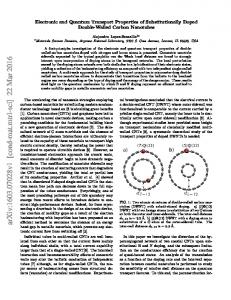
precursors used in the synthesis [20], band gap energy of the materials differed from the theoretical value (using analytical expression Eg =2.337 + 0.72x + 0.563x2 for x=0.25, 0.75 [21]. The inter-digitated array electrodes were fabricated using standard optical lithography on a SiO2 (250 nm thick)/Si wafer followed by deposition of Cr (5 nm)/Au (25 nm) and lift off in acetone. The channel width was W=200 m while the effective channel lengths L were 5, 9 and 17 µm. The width of each electrode was 5 µm. The NW film was made using a standard drop casting method. The NWs in chloroform were ultra-sonicated for 10 minutes prior to drop casting. A small drop (1 µl) of solution was drop casted in the center of the sample containing source and drain electrodes. The sample was left to dry at atmosphere before electrical characterization at a probe station. The film thickness was about 175 nm. Figure 1(c) shows a schematic of our devices including transport measurement setup. The room temperature dc transport measurements of the NW films were carried out at ambient condition using a standard two-probe technique both in dark and under illumination by a xenon lamp from a solar-light simulator (Oriel 96000) with a maximum power of 300 W. The light source was placed 10 cm above the sample and the intensity was measured with a calibrated silicon photodiode. The intensity of the light source was varied from 0 to 464 mW/cm2. The I-V characteristics in the dark and under illumination were measured using Keithley 2400 source meter and a current preamplifier (DL instruments: Model 1211) capable of measuring sub pA signal. These instruments were interfaced with LabView for data collection. 3. Results and Discussions: Figure 2(a) shows the I-V characteristics for Cd0.25Zn0.75S film with channel length L=5 µm under white light illumination with intensities of 51, 102, 165, 236, 322, 373, and 464 mW/cm2. The dark I-V curve is shown in the inset of figure 2(a). In the dark, the NW is highly insulating with a current of only 35 pA at 20 V bias. As the NW film was illuminated, the photocurrent is enhanced. The I-V curve shows nonlinear behavior with increasing bias voltage. At a fixed bias voltage, the photocurrent increases with increasing intensity. At the highest intensity of 464 mW/cm2 in our measurements, the photocurrent (Iphoto) at 15 V was 203 nA while the dark current (Idark) was only 20 pA resulting in an enhancement of photocurrent (Iphoto/Idark) of ~104. In order to check whether there was any effect of temperature due to this high intensity, we monitored the temperature of the film using a thermocouple. The temperature of the film increased from 25oC to 35oC when illuminated at the highest intensity of 464 mW/cm2. We then measured the dark I-V characteristics by heating the sample at 35oC. There was no change in the dark I-V curve compared to the room temperature dark I-V curve due to this heating effect. In other words, the observed photoresponse of up to 4 orders of magnitude is not affected by a small change of temperature under light illumination. Similar enhancement of photocurrent under white light illumination has been observed for other samples with x=0, and x=0.75. The UV-VIS absorption data in figure 1(b) shows that the absorption changes from 350 nm for Cd0.25Zn0.75S up to 600 nm for CdS. It can also be seen that the absorbance is almost the same for all the materials at peak wavelength. In our study, we used a white light from a solar simulator which covers all the wavelengths that the NW absorbs. Therefore similar photoresponse behavior under white light illumination is expected in our study.
3
Photocurrent (nA)
4
Photocurrent (nA)
Photocurrent (nA)
Figure 2(b) shows the photocurrent versus intensity for the same sample 300 (a) presented in figure 2(a), with different 200 electrode separations. As the intensity is increased, the photocurrent is increased from 100 0.01 to 10.96 nA for 17 µm, 0.02 to 60.15 nA 0 51(mW/cm2) for 9 µm, and 0.02 to 203 nA for 5 µm 102 -100 electrode separation. The dependence of 165 photocurrent on intensity can be described 236 -200 322 using a power law relation; I A P where 373 -300 A is a constant, P is the power of illumination 464 -20 -10 0 10 20 and is the exponent characterizing charge Voltage (V) transport in the semiconductor film. The circles are experimental points and the solid 200 (b) lines are fits to the power law equation. From L = 5 m V = 15 V the fit, we obtained A 1.4, 0.82 for 5 150 A = 1.4, = 0.82 µm, A 0.43, 0.60 for 9 µm, and A 0.023, 0.86 for 17 µm channel 100 L = 9 m length. The value of θ