JOURNAL OF APPLIED PHYSICS 108, 123509 共2010兲
Adhesion and cyclic stretching of Au thin film on poly„dimethyl-siloxane… for stretchable electronics Onobu Akogwu,1,2,a兲 David Kwabi,1,2 Auxillia Munhutu,1,3 Tiffany Tong,1,3 and W. O. Soboyejo1,2 1
Princeton Institute of Science and Technology of Materials (PRISM), 70 Prospect Street, Princeton, New Jersey 08544, USA 2 The Department of Mechanical and Aerospace Engineering, Princeton University, 1 Olden Street, Princeton, New Jersey 08544, USA 3 Department of Electrical Engineering, Princeton University, 1 Olden Street, Princeton, New Jersey 08544, USA
共Received 28 April 2010; accepted 2 October 2010; published online 21 December 2010兲 This paper presents the results of an experimental study of the effects of cyclic damage and adhesion on nanoscale Au thin films deposited on a flexible poly共dimethyl-siloxane兲 substrate. The deformation and cracking mechanisms are elucidated as functions of film thickness. The implications of the results are also discussed for the design of stretchable electronic structures. © 2010 American Institute of Physics. 关doi:10.1063/1.3510488兴 I. INTRODUCTION
Emerging applications in foldable and stretchable electronics fabricated on compliant polymer substrates are being developed for many applications that include electronic textiles,1 sensitive artificial skins,2 and foldable displays.3,4 Part of the motivation for such applications is the low cost and weight savings, portability, and potential for integration into other devices.5 Typically, foldable and stretchable electronic structures consist of layered polymer substrates on which functional circuits are fabricated with stiff materials and interconnected by metal thin film metal layers. Upon the application of tensile or compressive loads, the stiff circuits experience small strains, while the metal interconnects deforms uniformly with the substrate. Reports further show that thin metal films, either free-standing or supported by a polymer, can rupture at small strains 2%.6–12 It also been reported that certain polymer-supported well bonded metal films can sustain strains up to 20%.13 Other reports have established that, under tensile strains that are large enough to break surface passivation layers, dislocations readily escape from the metal film.14 It is also been suggested that further straining of the film does not result in strain hardening, which usually occurs in bulk films.15,16 Instead, weak interfaces between the film and the substrate may fail, or localization of deformation may occur as the film thins down until final rupture. Such localized necking, which occurs due to the Poisson effect and volume conservation, leads to a local elongation of film that is proportional to the thickness of the film.16 Although it has been shown that thin films deposited on a polymer substrate can benefit from the deformation restraint offered by the substrate,15 these authors are unaware of prior studies of the adhesion and cyclic loading on the failure mechanisms in Au thin films deposited on stretchable substrates, such as poly共dimethyl-siloxane兲 共PDMS兲. a兲
Electronic mail:
[email protected].
0021-8979/2010/108共12兲/123509/6/$30.00
In this section, we examine the adhesion and cyclic stretching of Au thin films deposited on PDMS. The influence of cyclic stretching on the failure is quantified by measurements of film electrical resistance. Cyclic deformation is shown to result in the accumulation of grain boundary and interfacial cracks in Au/PDMS structures. Experimental evidence of channel cracks, film buckling, and delamination are also presented from high resolution scanning electron microscopy 共SEM兲.
II. EXPERIMENTAL A. Adhesion
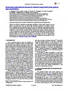
The adhesion between Au thin films and the PDMS substrates was measured using atomic force microscopy 共AFM兲 technique.18,22,23 Contact AFM tips from Veeco Instruments 共Woodbury, NY兲 were electron beam coated with 5 nm chromium and 50, 75, and 100 nm gold. The contact AFM experiments were performed in air, over a temperature range of 22– 25 ° C and relative humidity range between 31% and 46%. At least ten force curves were collected for each interaction using a Digital Instruments Dimension 3100 AFM 共Digital Instruments, Plainview, NY兲. The stages of the AFM adhesion tests are shown schematically in Fig. 1. The stiffness of each tip was measured using the thermal tune method.17 This was carried out with a Digital Instruments Nanoscope IIIa AFM 共Digital Instruments, Plainview, NY兲. In this way, the spring constants of the individually-coated tips were obtained, and used in he calculation of the adhesion forces. Since AFM measurements are highly sensitive to surface roughness, the tip radii and substrate roughnesses were measured for each experiment. The tip radii were calculated from tip profiles captured with a SEM 共Philips FEI XL30 FEGSEM, Hillsboro, OR兲. The measurement of the tip radii was done before and after AFM characterization to account for the potential effects of tip deformation during the course of
108, 123509-1
© 2010 American Institute of Physics
123509-2
J. Appl. Phys. 108, 123509 共2010兲
Akogwu et al.
FIG. 1. 共Color online兲 Schematic force displacement curve depicting the various stages 共A–E兲 of cantilever-surface engagement.
the experiments. Further details on the AFM adhesion measurement techniques are presented in Ref. 18.
where k is the spring constant of the AFM tip and x is the vertical displacement of the tip during lift-off from the sample surface.
B. Cyclic deformation
The cyclic deformation experiments were conducted in an Instron Model 5848 Microtester machine instrumented with a 50 N load cell 共Instron, Canton MA兲. The dog-bone specimens were deformed cyclically at a stress ratio R = min / max, of 0.001, where is the stress applied and the subscripts min and max correspond, respectively, to the minimum and maximum loads in the fatigue cycles. During cycling, the film resistance was measured using a Keithley Sourcemeter 共Keithley Corporation, Cleveland OH兲 with LABVIEW 共National Instruments, Austin, TX兲 Data Acquisition Measurement System, with probes connected across the gauge section 共3 mm兲 of our specimen Fig. 2. In this way, the evolution of film resistance was monitored as a function of cyclic loading. The cyclic tests were continued until 100 cycles were applied to each specimen.
B. Adhesion energies
The Derjaguin–Muller–Toporov 共DMT兲 model was used to quantify the adhesion energy across the interfaces, as shown in Fig. 4. The DMT model was used to characterize weak the interactions between stiff materials with small radii. This model relates the adhesion energy, ␥DMT to the adhesion force, Fadhesion via:
␥DMT =
Fadhesion , 2R
共2兲
where R is the effective radius, consisting of the AFM tip radius, Rtip, the root-mean squared roughness, Rrms of the surface of the sample. This is given by: R=
冉
1 1 + Rtip Rrms
冊
−1
共3兲
III. MODELING A. Adhesion forces
C. Crack driving forces
The adhesion force between the Au thin films and the PDMS substrate can be quantified using measurements of pull-off displacements 共Fig. 1兲 and the thermal tune tip stiffness measurements. The adhesion force was obtained from Hooke’s law to be:
From a fracture mechanics perspective, the adhesion energy, ␥DMT corresponds to critical mode I energy release rate, G. For crack growth between two dissimilar materials 共1 and 2兲 with surface energy 1 共␥surface1兲 and surface energy 2 共␥surface2兲, the adhesion energy, ␥DMT 关Eq. 共2兲兴 was equated to the mode I energy.18 Since adhesion is the inverse of fracture, the release rate can be expressed as:
Fadhesion = − ⫻ x,
共1兲
Gadhesion ⬇ Gelastic = ␥surface1 + ␥surface2 − ␥surface1–2 . 共4兲 For debonding of a metal film from the polymer substrate that is loaded uniformly in tension at fixed strain, ⑀app, the energy release rate can be expressed as:15 Gcrit =
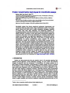
FIG. 2. 共Color online兲 Photograph of the tensile stage showing probes connected to the gauge section of sample. Set up was used to measure the film resistance during tensile cyclic loading.
2 ⬘ ⑀app Eau tau f共⌺, 兲, 2
共5兲
where E⬘ = E / 1 − 2, ⌺ = E⬘f / Es⬘, = tau / tPDMS, f共⌺ , 兲 = 共⌺3 + 1 / ⌺24 + 4⌺ + 6⌺2 + 4⌺3 + 1兲, Gcrit is the critical energy release rate of cracks in thin films, is the Poissons ratio, ⑀app is the nominal strain that is used to represent the applied load, tau is the Au film thickness, and E is the Youngs modulus of the film.
123509-3
J. Appl. Phys. 108, 123509 共2010兲
Akogwu et al.
Given that Gcrit ⬇ ␥DMT and because the PDMS substrate is infinitely thick 1 mm compared to the Au film 共50, 75, and 100 nm兲, i.e., tends to zero, f共⌺ , 兲 tends to 1 such that: 2 2 ⬘ ⑀app Eau tau cric tau ⬇ ⬇ ␥. 2 E⬘
Gcrit =
共6兲
For a smooth PDMS with an unbuckled Au film, at any temperature below the deposition temperature, Td ⬃ 50 ° C, the film is in a state of equibiaxial compressive stress 共the residual stress兲. The residual stress, 0, due to the considerable mismatch in coefficients of thermal expansion of Au共␣au兲 and PDMS 共␣PDMS兲,19 is given by:
0 =
再
冎
Eau共␣PDMS − ␣au兲共Td − T兲 , 共1 − au兲
共7兲
where ␣ represents the coefficients of thermal expansion, E is the Young’s modulus with EPDMS = 1.8 MPa 共from our tensile tensile tests, and Eau ⬃ 82 GPa. Based on data,19 ␣PDMS ⬇ 20␣au. Also is the Poisson ratio, with au = 0.33 and PDMS = 0.48, respectively.19 After film deposition, as the temperature drops to room temperature 共lower than deposition temperature, Td兲, buckling initiates when maximum principal compressive stress attains the critical value, c.19,20 Below this critical stress level, no buckling initiates within the Au film. For buckling of a film on a polymer layer, the critical stress c is expressed20 as:
再
crit ⬇ 0.52
Eau 2 共1 − au 兲
冎再 1/3
EPDMS 2 共1 − PDMS 兲
冎
2/3
,
共8兲
where the critical stress is a function of the properties of film and substrate independent of the deposition temperature, Td, unlike the residual stress, 0. Based on the significant difference between the stiffness of the Au film and the PDMS substrate, the wavelengths of the buckles are expected to be much greater than the film thicknesses.19 Another approach to quantify the critical stress for film buckling, c, is to employ a technique based on the wavelength, of the film buckles obtained from microscopy images such as AFM or SEM through the use of the following relations: per =
再
2 42Eautau 2 12共1 − au 兲
冎
1/2
,
共9兲
where per is the periodic wavelength of the buckled Au layer on PDMS. Hence, by measuring this wavelength of the Au herringbone wave patterns on PDMS,19,20 an estimate of crit is obtained, by rearranging Eq. 共9兲 to obtain:
crit =
再
2 42Eautau 2 122per共1 − au 兲
冎
.
FIG. 3. 共Color online兲 Measured adhesion force 共nanonewton兲 between the interfaces for Au/Cr/PDMS structures.
tive contributions of the residual and applied stresses to the development of critical conditions for final fracture. IV. RESULTS AND DISCUSSION A. Adhesion forces and energies
The measured pull-off displacements and AFM tip stiffnesses were used to calculate the adhesion forces between the different layers in the Au/PDMS structures with Cr interlayers. The resulting adhesion forces are presented in Fig. 3. The adhesion forces reveal a relatively strong interface between PDMS and the chromium 共Cr兲 interlayer. Furthermore, the interface between Cr and Au is stronger than that between PDMS and Au with no interlayer. Similar trends are observed when the adhesion forces obtained from Eq. 共2兲 are compared in Fig. 3. From these measurements, there is a substantial increase in adhesion force between Au/Cr/PDMS 共⬃67 nN兲 compared to Au/PDMS 共⬃10 nN兲. The corresponding adhesion energies obtained from the DMT model 关Eq. 共2兲兴 are presented Fig. 4. These again show the strong effect of Cr interlayers on the overall adhesion between Au and PDMS. B. Cyclic deformation and cracking of thin films
It has been shown that once a metal film debonds from the substrate 共becomes free-standing兲, the substrate no longer suppresses strain localization.16 In addition, prior theoretical work15,16 predicted that a compliant substrate with modulus in the megapascal range does not offer significant constraint to a well bonded metal film. However, from our experiments, the compliant PDMS 共E ⬃ 1.8 MPa兲 substrate does offer rea-
共10兲
Finally, it is important to note that the critical stress, crit, can be assumed to be the sum of the residual stress, res, and the applied stress, app. This gives:
crit = res + app .
共11兲
Equation 共11兲 applies to elastic films in which linear superposition can be applied. It can be used to assess the rela-
FIG. 4. 共Color online兲 Measured adhesion energy 共joule per meter square兲 between the interfaces for Au/Cr/PDMS structures.
123509-4
Akogwu et al.
J. Appl. Phys. 108, 123509 共2010兲
FIG. 6. 共Color online兲 SEM images showing the evolution of cracking phenomena in 50 nmAu/PDMS Structures Increase in crack widths and density resulted in increase in average film resistance 共a兲 before cycling, film morphology showing herringbone shaped wrinkling of the gauge section after evaporation 共b兲, channel cracks develop pervade the entire gauge section 共c兲, and channel cracks bridge and coalesce 共d兲 extensive cracking of film lead to film buckling and partial debonding.
FIG. 5. 共Color online兲 Variation in measured Au thin film resistance with number of loading cycles. 共a兲 50 nm Au thin film, 共b兲 75 nm Au thin film, and 共c兲 100 nm Au thin film.
sonable constraint to suppress strain localization that results in necking of films. This constraint we observed to be particularly effective at tensile strains less than 50%. Within the 50% strain regime, the deformation of PDMS is elastic. Cyclic deformation resulted in an increase in film resistance that increased with increased film thickness and cycling 关Figs. 5共a兲–5共c兲兴. Also, the as deposited Au films have a herringbone morphology 共Figs. 6–8兲 that is as a result of residual stresses due to misfit strains between film and substrate after deposition at high temperatures and cooling to room temperature. From the measured values of the critical wavelengths from SEM images 关Figs. 6共a兲, 7共a兲, and 8共a兲兴, Eqs. 共9兲 and 共10兲 were used to calculate the critical buckling stresses for the different film thicknesses. These results are shown in Table I. Furthermore, from Eq. 共6兲, the critical energy release rate, G, for the films were estimated as shown in Table I. The Gcrit calculated increases with increasing film thickness. Also, the values of Gcrit obtained from the analyses of the herringbone buckles 共Table I兲 are comparable to the measured values of surface energy 共2649 J / m2兲 obtained for Au/Cr interface using AFM techniques. The deposited Au/PDMS structure were initially loaded beyond the linear regime to determine a critical strain for
failure, which we quantified using the initial jumps in film electrical resistance been measured at time of loading. The strains are presented in Table II. Once these critical strains were determined, the different Au film thickness were cycled at their critical strains. From these experiments, the thinner films exhibited higher critical strains than the thicker films. Tunnel cracks 共traversing the entire gauge section兲 were the observed dominant types of cracks, as shown in Figs. 6–8 for 30 cycles of loading. These tunnel cracks resulted largely from subcritical crack growth along the grain boundaries. However, they were generally oriented perpendicular to the loading direction. However, the growth of these cracks can be modeled using expressions developed from earlier work by Suo and co-workers.21
FIG. 7. 共Color online兲 SEM images showing the evolution of cracking phenomena in 75 nmAu/PDMS structures. 共a兲 Before cycling showing some herringbone shaped wrinkling of the gauge section after evaporation, 共b兲 channel cracks develop and dominate as major damage mechanism, and 共c兲 channel cracks bridge and coalesce into grain boundary cracks. Partial debonding becomes significant 共d兲 grain boundary cracks leads to film buckling and extensive delamination.
123509-5
J. Appl. Phys. 108, 123509 共2010兲
Akogwu et al.
TABLE II. Effect of film thickness on measured critical strain and number of cycles to film rupture.
FIG. 8. 共Color online兲 SEM images showing the evolution of cracking phenomena in 100 nmAu/PDMS structures. 共a兲 Before cycling showing some herringbone shaped wrinkling of the gauge section after evaporation, 共b兲 channel cracks develop and increase in density, and 共c兲 channel cracks bridge and coalesce into grain boundary cracks. Partial debonding is pervasive 共d兲 grain boundary cracks leads to film buckling and complete delamination.
Also upon further cycling, an increase in the density of these cracks was observed. Since the critical energy release rate, Gcrit, scales with film thickness 关Eq. 共6兲兴, higher crack driving forces are needed in the thicker films. Hence, a higher level of cracking would be expected in the thicker films than the thinner films. The applied stresses at the onset of crack growth, app, would also be affected by the residual stresses, res, which are a function of film thickness. During each cycle, the films were loaded to critical strains and unloaded to initial strain 共0%兲. It was noted that the final resistance levels were higher than the initial values before loading after a few cycles. In addition, the increase in film electrical resistance at the critical strain 共in Table II for the different film thicknesses兲 was used to quantify the number of cycles to failure. Where failure is the point where the resistance value was stably in the tens of kilo ohms, compared to initial values in tens of ohms. These grain boundary cracks led to film delamination, after sufficiently large number of cycles were reached, as shown in Figs. 7 and 8. The increase in film resistance levels at after each cycle is a measure of the irreversible damage due to fatigue loading. Hence, the increase in resistance levels during loading is attributed to the opening of cracks, while the decrease in resistance in the unloading phase is associated with the closing of cracks. Although such opening and closing of cracks TABLE I. Variation in critical wavelength, buckling stress, and energy release rate with Au thin film thickness.
Film thickness 共nm兲
Measured critical wavelength 共m兲
Critical buckling stress 共MPa兲
Energy release rate 共J / m2兲
50 75 100
21.60 21.17 20.61
6.48 3.79 1.78
2300 3450 4601
Thickness of Au film 共nm兲
Measured critical strain 共%兲
Number of cycles
50 75 100
61 52 38
55 41 30
may be considered to be reversible phenomena until film delamination becomes pervasive after significant loading cycles, it is clear that the accumulation of such cracking/ damage occurs on a cycle-by-cycle basis. This leads ultimately to mechanical or electrical failure of the thin films intended for stretchable electronic applications. V. IMPLICATIONS
In stretchable electronics applications, large strain deformation will typically occur at strains that are sufficient to induce cracking. Furthermore, as the devices are likely to be used repetitively, the possible effects of fatigue loading should be considered in the design of Au/PDMS structures. These will require the further development of mechanismbased fatigue models for fatigue life prediction for the Au thin films deformed under cyclic loading. Furthermore, based on our experimental observations, there is a need for grain boundary engineering of Au thin films to improve their resistance to cracking. This may be achieved by the use of minor alloying and novel deposition techniques, such as soft contact lamination that may be used to to minimize the initial residual stresses. VI. CONCLUSIONS
This section presents measurements of adhesion and observations of cracking phenomena in Au/Cr/PDMS structures deformed under cyclic loading conditions. The use of Cr interlayers was shown to give rise to significant improvements in adhesion forces and energies. The cyclic stretching of the Au films was also shown to result in a range of cracking phenomena. These include: tunnel cracks due to grain boundary cracking, film buckling and delamination in the final stages of fatigue. The accumulation of such cracks resulted in increasing film electrical resistance with increasing cyclic stretching. The increase in film resistance was shown to be more severe in Au-PDMS structures with thicker Au films. The changes in film resistance, representative of functionality, could compromise the performance of devices fabricated on PDMS at large strains after substantial fatigue cycles. ACKNOWLEDGMENTS
The research supported by a grant from the Division of Materials Research of The National Science Foundation 共Grant Nos. DMR 0231418 and 0819860兲. Appreciation is extended to the Program Managers, Dr. Carmen Huber and Dr. Danielle Finotello, for their encouragement and support.
123509-6
Akogwu et al.
The authors will also like to thank Dr. Joyelle Jones-Harris, Mr. Joe Palmer, Wali Akande, and Ismaiel Yakub for useful technical discussions. E. Bonderover and S. Wagner, IEEE Electron Device Lett. 25, 295 共2004兲. V. J. Lumelky, M. S. Shur, and S. Wagner, IEEE Sens. J. 1, 41 共2001兲. 3 S. R. Forrest, Nature 共London兲 428, 911 共2004兲. 4 J. A. Rogers, Z. Bao, K. Baldwin, A. Dodabalapur, H. Katz, K. Amundon, J. Ewing, and P. Drzaic, Proc. Natl. Acad. Sci. U.S.A. 98, 4835 共2001兲. 5 A. Nathan and B. R. Chalamala, Proc. IEEE 93, 1235 共2005兲. 6 D. W. Pashley, Proc. R. Soc. London, Ser. A 255, 218 共1960兲. 7 H. Huang and F. Spaepen, Acta Mater. 48, 3261 共2000兲. 8 Y. Xiang, X. Chen, and J. J. Vlassak, Thin Films: Stresses and Mechanical Properties IX, MRS Symposia Proceedings No. 695 共Materials Research Society, Pittsburgh, 2002兲, p. 189. 9 H. D. Espinosa, B. C. Prorok, and B. Peng, J. Mech. Phys. Solids 52, 667 共2004兲. 10 S. Chiu, J. Leu, and P. S. Ho, J. Appl. Phys. 76, 5136 共1994兲. 11 B. E. Alaca, M. T. A. Saif, and H. Sehitoglu, Acta Mater. 50, 1197 共2002兲. 12 Y. Xiang and J. J. Vlassak, Scr. Mater. 53, 177 共2005兲. 13 P. Gruber, J. Bohm, L. Sauter, R. Spolenak, and E. Artz, Nanoscale Ma1 2
J. Appl. Phys. 108, 123509 共2010兲 terials and Modeling-Relations Among Processing, Microstructure and Mechanical Properties, MRS Symposia Proceedings No. 821 共Materials Research Society, Pittsburgh, 2004兲. 14 T. Li, Z. Y. Huang, S. P. Lacour, S. Wagner, and Z. Suo, Mech. Mater. 37, 261 共2005兲. 15 T. Li, Z. Y. Huan, Z. Suo, S. P. Lacour, and S. Wagner, Appl. Phys. Lett. 85, 3435 共2004兲. 16 Y. Xiang, T. Li, Z. Suo, and J. J. Vlassak, Appl. Phys. Lett. 87, 161910 共2005兲. 17 In Rev, AO; Vol. AN 90 Veeco Instruments Inc., 2005. 18 T. Tong, B. Babatope, O. Akogwu, W. Akande, and W. O. Soboyejo, J. Appl. Phys. 106, 083708 共2009兲. 19 N. Bowden, S. Brittain, A. G. Evans, J. W. Hutchinson, and G. M. Whitesides, Nature 共London兲 393, 146 共1998兲. 20 J. Kim and H. H. Lee, J. Polym. Sci., Part B: Polym. Phys. 39, 1122 共2001兲. 21 J. W. Hutchinson and Z. Suo, Adv. Appl. Mech. 29, 63 共1991兲. 22 N. Rahbar, A. Orana, K. Wolf, C. Marynhoff, and W. O. Soboyejo, J. Appl. Phys. 104, 103533 共2008兲. 23 Z. Zong, Y. Cao, N. Rahbar, and W. O. Soboyejo, J. Appl. Phys. 100, 104313 共2006兲.