Accepted Manuscript Title: Influence of Nitrogen Flow Rate on Microstructural and Nanomechanical Properties of Zr-N Thin Films Prepared by Pulsed DC Magnetron Sputtering Author: Akash Singh P. Kuppusami Shabana Khan C. Sudha R. Thirumurugesan R. Ramaseshan R. Divakar E. Mohandas S. Dash PII: DOI: Reference:
S0169-4332(13)00825-8 http://dx.doi.org/doi:10.1016/j.apsusc.2013.04.107 APSUSC 25576
To appear in:
APSUSC
Received date: Revised date: Accepted date:
30-11-2012 19-4-2013 19-4-2013
Please cite this article as: A. Singh, P. Kuppusami, S. Khan, C. Sudha, R. Thirumurugesan, R. Ramaseshan, R. Divakar, E. Mohandas, S. Dash, Influence of Nitrogen Flow Rate on Microstructural and Nanomechanical Properties of Zr-N Thin Films Prepared by Pulsed DC Magnetron Sputtering, Applied Surface Science (2013), http://dx.doi.org/10.1016/j.apsusc.2013.04.107 This is a PDF file of an unedited manuscript that has been accepted for publication. As a service to our customers we are providing this early version of the manuscript. The manuscript will undergo copyediting, typesetting, and review of the resulting proof before it is published in its final form. Please note that during the production process errors may be discovered which could affect the content, and all legal disclaimers that apply to the journal pertain.
Influence of Nitrogen Flow Rate on Microstructural and Nanomechanical Properties of Zr-N Thin Films Prepared by Pulsed DC Magnetron Sputtering
cr
ip t
Akash Singh, P. Kuppusami*, Shabana Khan, C. Sudha, R. Thirumurugesan, R. Ramaseshan a,R. Divakar, E. Mohandas, S. Dasha Physical Metallurgy Group, Indira Gandhi Centre for Atomic Research, Kalpakkam-603 102, India a Surface and Nano Science Division, Indira Gandhi Centre for Atomic Research, Kalpakkam 603 102, India
us
Abstract
an
Zr-N thin films were deposited on Si (100) substrate by reactive sputtering using a pulsed DC magnetron sputtering technique. It was found that films deposited at 773 K and 1
M
sccm of nitrogen flow rate show a single phase with face centred cubic-ZrN. Raman analysis also confirmed the formation of ZrN phase in the films. The films deposited at
d
nitrogen flow rate greater than 1 sccm show ZrN along with orthorhombic-Zr3N4. The
te
chemical bonding characteristics of the films were analyzed by X-ray photoelectron
Ac ce p
spectroscopy. High resolution transmission electron microscopy also gave evidence for fcc- ZrN and o-Zr3N4 phase and revealed equiaxed grains in these films. In addition, hardness
and Young’s modulus of the films measured as a function of nitrogen flow
rate is discussed qualitatively in relation to resistance to plastic deformation offered by these films.
Keywords: Magnetron sputtering; Zirconium nitride, X-ray diffraction, X-ray photoelectron spectroscopy, Transmission electron microscopy, Hardness. *Corresponding author: Email :
[email protected] Fax: 91-44-27480121;Tel :91-4427480500-22630
Page 1 of 28
Introduction Transition metal nitrides and oxy-nitrides are very attractive compounds because of their excellent mechanical, thermal, electrical and catalytic properties [1]. AlN for
ip t
example, possesses a high electrical resistivity, a good thermal conductivity and stability up to very high temperatures [2]. These properties make it very interesting for
cr
microelectronic devices. TiN combines characteristics of both covalent compounds, such
us
as extreme hardness and high melting point, and of metallic compounds such as good thermal and electrical conductivity [3,4]. TiN is extensively used in cutting tools and by
an
coating industries. Concerning catalytic activity of nitrides, molybdenum nitride is known to be active in dehydronitrogenation of pyridine and on the Al-P-O-N oxynitride
surface properties. Also, Zr-N have been extensively
d
during nitridation influences
M
catalysts[5]. Massinon et al. [6] have shown that the substitution of oxygen by nitrogen
te
studied for industrial applications as hard coatings [7,8], diffusion barrier in semiconductor technology [9-11], optical applications for heat mirrors [12-16] and
Ac ce p
decorative coatings [17-20] because of their outstanding properties. The optical and mechanical properties of ZrN have been reported to depend on nitrogen composition [2123]. For instance, the stoichiometric ZrN is metallic-like with a golden color and is a thermodynamically
stable phase. Whereas Zr3N4 compound is a metastable phase,
insulating in nature and almost transparent [23]. ZrN is known to be a good reflective material in the IR wavelength range [24] due to the metallic structure of the stoichiometric ZrN. Although nitrides are thermodynamically stable, they are readily oxidized even at room temperature [25-26]. This oxidation or contamination by oxygen can be a major problem (or can be intentional, i.e. passivity of samples) since it
Page 2 of 28
completely modifies the properties and reactivities of the solids. It is also evident that the microstructure and properties of ZrN film vary with different deposition techniques and processing parameters [27-29]. such as
evaporation, spray
ip t
Thin films are deposited by various methods
pyrolysis, pulsed laser deposition, sol-gel, electron beam evaporation, chemical vapour
cr
deposition and sputtering. In the present work, an investigation on sputter deposited Zr-N
us
films on Si (100) from a zirconium target in a mixture of Ar/N2 pulsed direct current (DC) magnetron discharges is carried out. In the magnetron sputtering, the ion
an
bombardment is well known to modify the film structure, to improve the film properties and to increase the film density [30-34]. Pulsed DC magnetron sputtering process has
M
become an attractive production deposition technology. The technique is capable of
d
reducing arcing event, which results from charge accumulation on target surfaces. It
te
consequently prevents the deterioration of film properties and maintains a stable deposition process. The physical properties of Zr-N films prepared by pulsed DC
Ac ce p
magnetron sputtering mainly depend on process
parameters. For instance, we have
recently reported the effect of substrate temperature on the tribological behavior of ZrN thin films [35]. Since
some of the physical properties of zirconium nitrides highly
depend on the microstructure and nitrogen content of the films, the effect of nitrogen flow on the microstructure and nanomechanical properties is investigated in the present study. Experimental Procedure A zirconium target ( purity better than 99.9%) of 76 mm diameter and 2 mm thickness was used to deposit zirconium nitride films on to Si (100) substrates and
Page 3 of 28
titanium modified austenitic stainless steel (D-9 alloy). Si was chosen because of its wide application in electronic industry, while D-9 alloy is used as structural material for breeder reactors. The sputtering was carried out using a Mighty Mak US sputtering gun
ip t
of 3 inch diameter in a custom built magnetron sputtering system which consisted of a stainless steel chamber of 45 cm diameter and 20 cm deep. The deposition chamber was
cr
evacuated to a base pressure of 2× 10⁻⁵ mbar (at the deposition temperature of 773 K)
us
using a pumping system consisting of a rotary and turbo molecular pumps (Alcatel, France). Silicon substrates (size of 10 mm × 10 mm × 0.5 mm) were first cleaned using
an
soap solution and then ultrasonically cleaned in acetone for 15 minutes and dried by blowing hot air before being placed in the deposition chamber. The flow rate of the
M
argon (99.99% purity) was varied in the range 40-50 standard cubic centimeter per
d
minute (sccm) and the N2 (99.99% purity) flow rate was varied in the range 0-10 sccm
te
such that the total flow rate of the gases in the chamber during sputtering was 50 sccm. A RPG-50 asymmetric bipolar pulsed DC power supply (MKS instruments, USA) was used
Ac ce p
as the electrical power source for the sputter deposition. The substrate temperature was kept constant at 773 K using a halogen lamp (800W, 6.3 A) heater with a digital programmable temperature controller. Pre-heating of the substrate to a desired set temperature for about 0.5 h was carried out. Pre-sputtering of the target was performed for 5 minutes before each deposition. The deposition conditions and pulse parameters of the power source used in the present investigations are given in Table 1. The thickness of the films was measured using DEKTAK 6M-stylus profiler (Veeco, USA). Structural properties of the as deposited ZrN films were characterized by x-ray diffraction using an INEL (XRG – 3000, France) Diffractometer with glancing
Page 4 of 28
angle incidence (ω) of 5° and Cu Kα1 radiation. Monochromator with germanium crystal was used to eliminate CuKα2. The crystallite size was determined using the Scherrer’s formula. Structural information was also obtained by micro- Raman spectroscopy using
ip t
Horiba Jobin Yvon (HR 800, France) at wavelength of 514 nm with spectral resolution of 1 cm-1. X-ray photoelectron spectroscopy (XPS) was carried out in a
SPECS
cr
spectrometer operating at an anode voltage of 13 kV and power level of 300 W.
us
Monochromatic Al Kα was used as the primary source with an energy of 1486.6 eV at base vacuum better than 2.9 x 10⁻⁹ mbar. Ar ions at 5 kV and 50 µA were used for
an
sputtering the specimen surface. Spectra were collected using Specs Lab2 data analysis software and de-convolution of the spectra was performed using CASA XPS system
M
(version 2.3.13Dev30). For transmission electron microscopy (TEM) study, thin films of
d
Zr-N of thickness ~50 nm were deposited at 673 K on KCl crystal with varying nitrogen
te
flow rates (1 – 4 sccm). The films deposited on KCl crystal were dissolved in distilled water and some portions of the films were collected on holey carbon coated copper grids.
Ac ce p
TEM samples were prepared at 673 K due to the practical limitation of using KCl single crystal substrate at 773 K. We have not noticed any significant change in the crystallite size measured by XRD in the temperature range of 673 K to 773 K [36]. High resolution transmission electron microscopy (HRTEM) studies were carried
out on a Philips CM200 and JEOL 2000 EX II TEM operated at 200 kV. The nanohardness measurements of the films deposited on Ti modified austenitic stainless steel (D-9 alloy) [35] were carried out by means of a nanoindenter (CSM, Switzerland) equipped with a Berkovich diamond indenter tip at a load of 10 mN. Results and Discussion
Page 5 of 28
The Zr-N films were deposited at 773 K by reactive sputtering as a function of nitrogen flow rates in the range 0.5 to 10 sccm for a constant time of deposition of 60 minutes. The thickness, and obviously the deposition rate, was found to decrease with
ip t
increasing flow rate of nitrogen, but reaching a roughly constant value when nitrogen flow rate is equal or higher than 4 sccm (Fig. 1). Typical thickness of the films was in
cr
the range 0.4-0.8 µm. Films showed golden colour for the films deposited at nitrogen
rate > 1 sccm.
us
flow rates ≤ 1 sccm and exhibited light gray colour for those deposited at nitrogen flow XRD patterns (Fig. 2a) show that films deposited in pure argon
an
atmosphere are polycrystalline and exhibit hcp- α Zr phase with (002), (101), (102), (103), (200) and (112) reflections. It has been reported that the crystalline films of Zr
M
could be formed even at room temperature [36]. It is noticed that films deposited at lower
d
flow rates of nitrogen ( 1sccm) show (111), (200), (220) , (311) and (222) planes
te
corresponding to fcc- ZrN phase. The films deposited at nitrogen flow rates >1 sccm show broadening and reduction in the intensities of (111), (220) and (311) reflections.
Ac ce p
Also, the crystallite size of the films decreases with increasing nitrogen flow rate (Fig. 2b) due to structural disordering leading to amorphization. In our thin film deposition, the increase of nitrogen partial pressure was accompanied by the decrease of the partial pressure of argon in order to keep the total flow rate constant. As a result, the overall sputtering yield of the target decreased due to lower ionization of molecular nitrogen compared to argon, which causes a continuous decrease in the deposition rate of the films up to 4 sccm and then becomes constant (Fig.1). It is suggested that at higher nitrogen flow rates, distortions are produced in the lattice due to increased
Page 6 of 28
accommodation of nitrogen atoms. Therefore, the reduction in the crystallite size with increasing nitrogen flow rate could be related to tendency for amorphization.. The influence of nitrogen flow rate on the intensities of the peaks of Zr-N is also
ip t
noticed. The preferred orientation of the film as a function of nitrogen flow rate was assessed from the intensities corresponding to (111) and (200) planes of the Zr-N films.
cr
Films show (111) preferred orientation at nitrogen flow rates 0.5 sccm and show (200)
us
orientation at the nitrogen flow rates of 1 sccm. The film tends to become more polycrystalline with slight increase in the intensity for (111) reflection at the nitrogen
an
flow rate of > 1 sccm and show mixed orientation in flow rate range 2-6 sccm. The crystallite size of Zr deposited with pure argon was ~ 40 nm, and it decreases
M
from ~35 nm to ~10 nm with an increase in the nitrogen flow rate from 0.5 to 2 sccm
d
(Fig. 2b) and beyond that it remains constant. The above crystallite sizes were calculated and only the
te
using Scherrer’s formula which does not take strain into consideration strongest reflection of Zr and ZrN was used to determine the crystallite size.
Ac ce p
The lattice parameter a was found to be in the range 4.573-4.602 ±0.003 Å. It was
noticed that there is slight increase in the lattice parameter as a function of nitrogen flow rate as the excess nitrogen can preferentially occupy interstitial positions leading to a monotonous increase of the lattice parameter. In addition to the formation of ZrN phase, broad reflections of (111), (511) and (042) corresponding to o- Zr3N4 phase was identified in accordance with the JCPDS file no: 87-0843 [24,37]. As the nitrogen flow rate increases up to 10 sccm, the films are found to be poorly crystallized. This can be explained by the absence of the stable phases in the nitrogen rich zone of Zr-N system.
Page 7 of 28
Figure 3 shows the Raman spectra of the films deposited in the nitrogen flow rate range of 1 to 4 sccm. The spectra indicates the frequency band of 170 cm-1, 209 cm-1, 499 cm-1 , 710 cm-1 and 980 cm-1 of ZrN. The band positions obtained from the film is
ip t
found to be consistent with the reported values [38]. In a perfect fcc structure, first order Raman scattering is forbidden due to selection rules. However in this case due to disorder
cr
induced by the deposition technique, the translation symmetry is lost, and all the modes
us
can participate in the scattering. Raman spectra will be an “image” of the density of vibrational states (DVS) [39]. At low frequency range, the bands are attributed to the
an
disorder of single phonons and second order processes, whereas at higher frequencies the asymmetry of the bands is due to the superposed contributions of disorder of optical
M
phonons and second order combination of acoustic and optical processes [40]. In this case also the broadening of the bands indicate the disorder of the crystals. At higher nitrogen few bands (at 710 cm-1 and 980 cm-1) tend to disappear indicating
d
a
te
flow rates,
amorphization. The as-deposited ZrN film presents a Raman spectrum with the typical
Ac ce p
broadened bands, due to the disorder induced by N vacancies [41]. However in this case we could not get significant change as a function of nitrogen flow rate up to 4 sccm. Elements such as zirconium, nitrogen, oxygen, and carbon as a function of
nitrogen flow rates were identified in the films by assigning the corresponding XPS peaks. Fig. 4(a) is the representative XPS spectra of ZrN film deposited at 773 K and 1 sccm flow rate of nitrogen showing the photo electron peaks from Zr, N, O and C. After removing the surface contaminants through argon ion sputtering, the high resolution spectra were recorded for each individual photo electron peak. Fig. 4(b) and (c) show high resolution XPS spectra corresponding to Zr 3d and N 1s, respectively obtained after
Page 8 of 28
1 min sputtering. After deconvolution, the main Zr 3d peak was found to consist of individual peaks corresponding to ZrN and ZrO2. In addition, evidence is obtained for the contribution from a phase having chemistry intermediate between ZrN and ZrO2.
ip t
Comparing the binding energy values with the available information in literature on oxidized Zr-N films [42-44], this phase is found to be related either to an oxy-nitride
cr
such as Zr2N2O or nitride such as Zr3N4. Binding energy values for Zr, ZrN, ZrO2 and
us
Zr3N4 obtained in this study compare well with already reported values in the literature [45-50]. Based on similar analysis carried out on all the specimens, it was observed that
an
the metallic phase of Zr is present only at the nitrogen flow rate 1 sccm and a slight
M
shift in the binding energies of Zr-N is noticed at higher flow rates of nitrogen. High resolution N 1s spectra is found to be asymmetric with contribution from nitrogen
d
peaks corresponding to ZrN at 397.3 eV [45-48], Zr3N4 at 396.5 eV [46,48] and
te
elemental nitrogen at 398.6 eV [48-50]. The elemental nitrogen peak may correspond to adsorbed nitrogen. Zirconium deposited freshly on a substrate is found to react readily
Ac ce p
with O2, CO, CO2 and hydrocarbons, forming oxides and carbides which are essentially unreactive, and the gettering rate of zirconium for N2 is observed to be smaller than that for O2 [51-52]. Therefore, it is possible
that small amounts of Zr-O compounds could
form while depositing Zr-N in the present study. TEM studies show that the film deposited at the nitrogen flow rate of 1 sccm
reveal fcc-ZrN and small amounts of o- Zr3N4 phase of equiaxed nanocrystallites of sizes in the range 4-9 nm (Fig. 5 a). Diffraction pattern corresponding to first, fourth and sixth rings of the inset of Fig.5 (a) gave evidence of o- Zr3N4 phase (Table 2). However,
Page 9 of 28
Zr3N4 phase was not identified by XRD in the films deposited at 1 sccm flow of nitrogen due to its lower limit of detection upto 5wt %. The films deposited at 2 sccm are seen to be nanostructured with nanocrystallites
ip t
of sizes in the range 4-9 nm (Fig. 5 b). It is also seen that film contains fcc-ZrN and oZr3N4 phase and the polycrystalline diffraction patterns corresponding to these phases
cr
have been shown in the inset of Fig. 5 (b). First, fourth and sixth rings of the diffraction
us
pattern gave evidence for the presence of o-Zr3N4 phase. The zirconium nitride film deposited at 4 sccm of nitrogen flow rate was also seen to be nanostructured with and the film mostly contains fcc-ZrN
an
nanocrystallites in the range 4-9 nm (Fig. 5 c)
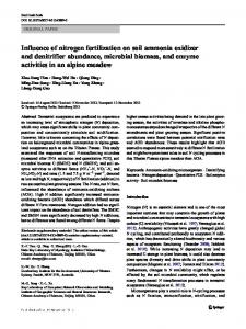
along with o- Zr3N4 phase and the diffraction pattern corresponding to these phases have are shown in Table 2. Fig. 6 shows the HREM
M
been indexed and the d-spacing
d
micrograph of the nanocrystalline thin film deposited at 4 sccm containing fcc-ZrN and
te
o- Zr3N4 nanocrystallites with crystallite sizes in the range 4 - 9 nm. It is also pointed out on the crystallite size obtained in TEM
XRD because the Scherrer formula used to calculate the
Ac ce p
than that obtained from
and XRD. TEM shows lower crystallite size
crystallite size does not take strain into account, though the X-ray peak broadening is caused by crystallite size and strain. Nanoindentation studies were performed to estimate the mechanical properties of
the films. The applied load for nanoindentor was selected such that the indentation depths were in the range from 40 to 80 nm in order to avoid the contribution from the substrate. The indentation load and displacement were continuously recorded during one complete cycle of loading and unloading [53] for measuring hardness and modulus of the films. The nanohardness and Young’s modulus were evaluated using the approach by Oliver
Page 10 of 28
and Pharr [54]. The load displacement response obtained by nanoindentation contains information about the elastic and plastic deformation of the films. The area between the loading and unloading curves represents the energy dissipation in the films due to plastic represents the elastic energy for
ip t
deformation. The area under the unloading curve
deformation. The hardness is derived from the peak hardness and projected area of
us
from the slope of the upper portion of the unloading curve [55].
cr
indentation, while reduced Young’s modulus is obtained from the stiffness measured
The nanohardness of Zr-N thin films deposited on D-9 alloy were measured as a
an
function of nitrogen flow rate from 0 to 10 sccm. This metallic material is softer (~2GPa) than Si substrate ( ~8-10 GPa) and is used as a clad material for breeder
M
reactors [35]. Also, the structural information of the films obtained from D-9 alloy is
d
similar to that on Si substrate. The average hardness and Young’s modulus values of Zr
te
films deposited in pure argon were 6.8 ± 2 GPa and 190 ± 25 GPa [56]. It is observed that the values of hardness and Young’s modulus of the Zr-N films were in the range of
Ac ce p
21-26 GPa ± 3 GPa and 300-440 GPa ± 52 GPa, respectively (Fig 7 (a) and (b)). However, these values are significantly higher than that of the bulk
hardness of ZrN
(14.7 GPa) reported in the literature [1]. The calculated value of the Young’s modulus from the present study is in agreement with that of To¨rok et al. [57], who have reported a value of 460 GPa from the flexural resonance frequency of the reactive magnetron sputtered coatings deposited on steel substrates. A protective film such as ZrN not only requires high hardness but also high resistance to plastic deformation during contact events. The ratio, H/E and H3/E2 have been increasingly applied to evaluate the resistance to plastic deformation from the values
Page 11 of 28
of H and E [58]. The increased value of H3/E2, gives information on the resistance of the material to plastic deformation. Fig. 7(c) shows the values of H/E and H3/E2 of the ZrN thin films as a function of nitrogen flow rate. In contrast to H3/E2 , the variation of H/E
has a value 0.01 ± .009 GPa for the films deposited in pure argon
ip t
is not very significant for the nitrogen flow rate ≥ 2sccm. However, H3/E2 of ZrN films and it increases to
cr
0.11 ± .009 GPa for the films formed at 1 sccm and then decreases to 0.095 ± .009 GPa
us
for 10 sccm of nitrogen flow rate. From the values of H3/E2, it is evident that Zr-N films deposited at 2 sccm of nitrogen flow rate could offer higher resistance to plastic
an
deformation. The variation in the resistance to plastic deformation could be discussed in terms of the microstructure. In the present work, the mean crystallite size is significantly
M
reduced as nitrogen flow rate is increased and this results in the increase in the hardness
d
value for the films deposited up to 2 sccm of nitrogen flow rate. However, above 2 sccm
te
of nitrogen flow rate, films show poor crystallinity and also the formation of impurity phase of Zr3N4. The present study indicates that the reduction in the value of resistance to
Ac ce p
plastic deformation at higher nitrogen flow rates may be related to the change in the microstructure, especially, the crystallite size and formation of secondary phase. Conclusions
The microstructural and nanomechanical properties of Zr-N films deposited on Si (100) substrate by pulsed DC magnetron sputtering as a function of nitrogen flow rates at the substrate temperature of 773 K has been investigated. Films deposited up to 1 sccm of nitrogen flow rate showed single phase fcc-ZrN, while films deposited at nitrogen flow rate > 1 sccm and up to 6 sccm revealed the growth of ZrN along with Zr3N4 secondary phase. Films deposited > 6 sccm has poor crystallinity. XPS analysis of these films indicated the presence of Zr, ZrN, ZrO2 and Zr2N2O phases. TEM studies also confirmed
Page 12 of 28
the presence of ZrN along with small amount of o-Zr3N4 phase at higher nitrogen flow rates. The effect of nitrogen flow rate on the nanomechnical properties indicated an and showed a peak value for the
us
cr
resistance to plastic deformation at lower flow rates of nitrogen .
ip t
enhancement in hardness and elastic modulus
an
Acknowledgements
The authors are thankful to Smt. M. Jyothi for substrate preparation and XRD analysis.
M
They are also grateful to Dr. M. Vijayalakshmi, Associate Director, PMG, Dr. T. Jayakumar, Director, Metallurgy and Materials Group and Shri. S. C. Chetal, Director,
Ac ce p
te
d
IGCAR for the support and encouragement.
Table 1: Deposition parameters of Zr-N thin films Base Pressure
:
2 x10⁻⁵ mbar
Operating Pressure
:
7.5 x10⁻³ mbar
Substrate to target Distance
:
60 mm
Target voltage
:
220 - 320 V
Substrate temperature
:
773 K
Pulse Power
:
100 W
Duty Cycle
:
20%
Pulse Frequency
:
100 kHz
Argon flow rate
:
50-40 sccm
Nitrogen flow rate
:
0-10 sccm
Page 13 of 28
ip t
Table 2 : Calculated d-spacings of ZrN and Zr3N4 phases from the selected area diffraction patterns of the films deposited at 1 and 4 sccm of nitrogen flow rate.
dexp (nm)
ZrN JCPDS# 650972
Zr3N4 JCPDS# 87-0843
2
0.261 0.2641
111
0.2606
3
0.224 0.2287
200
0.2256
4
0.177
-
5
0.159 0.1618
220
6
0.150
7
0.135 0.1379
8
0.130 0.1321
-
(hkl)
-
0.2988
111
111
0.302
211
0.266 0.2641
111
0.2638
211
131
0.232 0.2288
200
0.2355
131
0.1773
160
0.184
-
0.1838
421
0.1599
511
0.166 0.1618
220
0.1654
511
0.1503
360
0.157
-
0.1576
360
311
0.1349
042
0.140 0.1379
311
0.1402
042
222
0.1297
650
0.118 0.1143
400
0.1181
480
-
Ac ce p
-
-
d (nm)
M
0.2897
Zr3N4 JCPDS# 87-0843
d
-
0.289
te
-
(hkl)
1
ZrN JCPDS# 650972
d (nm) (hkl)
d (nm)
an
d (nm) (hkl)
dexp (nm)
us
Ring No.
Phases at nitrogen flow rate of 4 sccm
cr
Phases at nitrogen flow rate of 1 sccm
-
-
Page 14 of 28
References [1] L.E.Toth, L.E., Transition Metal Carbides and Nitrides. Academic Press, New York, (1971).
Coatings Technology 196 (2005) 130– 134.
cr
[3] K. Kamiya, T. Yoko, M. Bessho, J. Mat. Sci. 14 (1979)70.
ip t
[2] Zhenghua An, Chuanling Men, Zhengkui Xu, Paul K. Chu, Chenglu Lin, Surface &
us
[4] H. G. Tompkins, J. Appl. Phys.70 ( 1991) 3876.
[5] C. W. Colling, J.G. Choi, L. Thompson, J. Catal. 160 ( 1996) 3542.
P.Grange, Appl. Catal. A 137( 1996) 9.
an
[6] A.Massinon, J.A., Odriozola, Ph Bastians, R.Conanec, R. Marchand, Y. Laurent,
M
[7] W. D Sproul, J. Vac. Sci. Technol. A 4 ( 1986) 2874.
d
[8] J. Vetter, R. Rochotzki, Thin solid films 192 (1990) 253.
te
[9] S. Kanamori, Thin solid films 136 (1986) 195. [10] M. Ostring, S Nygren, C. S. Petersson, H. Norström, R. Buchta, H.O. Blom, S. Berg
Ac ce p
Thin solid films 145 (1986) 81.
[11] K. Hinode, Y. Homma, M. Horiuchi, T. Takahashi, J. Vac. Sci. Technol. A15 (1997) 2017.
[12] P. J. Matin, R. P. Netterfield, W. G Sainty, Vaccum 32 (1982) 359. [13] B. Karlsson, R. P. Shimshock, B. O. Serphin, Phys. Scr. 25(1982) 775. [14] B. Karlsson, C. G. Ribbing, SPIE 324 ( 1982) 52. [15] C. G. Ribbing, A. Roos, SPIE 3133 ( 1997) 148. [16] P. Panjan, A. Zabkar, B. Navinsek, et al., Vacuum 40, 161 (1990). [17] A. Mumtaz, W. H Class, J. Vac. Sci. Technol. 20 ( 1982) 345.
Page 15 of 28
[18] P. C. Johnson, H. Rawdhawa, Surf. Coat. Technol. 33 ( 1997) 53. [19] M. Molariur, A. S. Korhnen, E. Harju, R. Lappalainen, Surf. Coat. Technol. 33 (1987) 117.
ip t
[20] M. Nose, T. Nage, M. Yokota, S. Saji, M. Zhou, M. Nakoda, Surf. Coat. Technol. 116 (1999) 296.
cr
[21] L. Pichon, T. Girardeau, A. Straboni, F. Lignou, J. Perrie´re, J.M. Frige´rio, Nucl.
us
Instr. Meth. Phys. Res. B147 (1999) 378.
[22] B.O. Johansson, H.T.G. Hentzell, J.M.E. Harper, J.J. Cuomo, J. Mater. Res. 1 (1986)
an
442.
[23] M. Yoshitake, T. Yotsuya, S. Ogawa, Jpn. J. Appl. Phys. 31 (1992) 4002.
M
[24] L. Pichon, T. Girardeau, A. Straboni, F. Lignou, P. Gue´rin, J. Perrie`re, Appl. Surf.
d
Sci. 150 (1999) 115.
te
[25] A.D. Katnani, K.I. Papathomas, J. Vat. Sci. Technol. A5(4) ( 1987) 1335. [26] J.C. Francois, Y. Massiani, P. Gravier, J. Grimblot, L.Gengembre, Thin Solid Films,
Ac ce p
223 ( 1993) 223.
[27] S. Horita, M. Kobayashi, H. Akahori, T. Hata, Surf. Coat. Technol. 66 (1994) 318. [28] A.J. Perry, J.P. Schaffer, J. Brunner, W.D. Sproul, Surf. Coat. Technol. 49 (1991) 188.
[29] P.C. Johnson, H. Randhawa, Surf. Coat. Technol. 33 (1987) 53. [30] A. Lousa, E. Martinez, J. Esteve, E. Pascual, Thin Solid Films 35-356 (1999) 210. [31] A. Thobor, C. Rousselot, C. Clement, Jamal Takadoum, Nicolas Martin, Rosendo Sanjines, Francis Levy Surf. Coat. Technol. 124 (2000) 210. [32] T. Migita, R. Kamei, T. Tanaka, K. Kawabata, Appl. Surf. Sci. 169-170 (2001) 362.
Page 16 of 28
[33] J.F. Pierson, E. Tomasella, Ph. Bauer, Thin Solid Films 408 (2002) 26. [34] E. Ribeiro, A. Malczyk, S. Carvalho, et al., Surf. Coat. Technol.151-152 (2002) 515.
M.P. Srinivasan, E. Mohandas, A.K. Tyagi, Wear 280–281(2012) 22.
ip t
[35] Akash Singh, N. Kumar, P. Kuppusami, T.N. Prasanthi, P. Chandramohan, S. Dash,
[36] Akash Singh, M. Geetha, N. Kumar, P. Kuppusami, R. Thirumurugesan, E.
cr
Mohandas, V. Kamaraj, Transactions of the Indian Institute of Metals 64 (2011 ) 37.
us
[37] R. Lamni, E. Martinez, S.G. Springer, R. Sanjinés, P.E. Schmid, F. Lévy, Thin Solid Films 447 –448 (2004) 316.
an
[38] C.P. Constable, J. Yarwood, W.D. Mu¨nz, , Surf. Coat. Technol 116–119 (1999) 155.
M
[39] A.N. Christensen, O.W. Dietrich, W. Kress, W.D. Teuchert, Phys. Rev., B 19 (1979)
d
5699.
(2000) 13915.
te
[40] A. Cassinese, M. Iavarone, R. Vaglio, M. Grimsditch, S. Uran, Phys. Rev., B 62
Ac ce p
[41]C. Moura , P. Carvalho, F. Vaz, L. Cunha , E. Alves, Thin Solid Films 515 (2006) 1132.
[42] I. Milošev, H.-H. Strehblow, B. Navinšek, Thin Solid Films 303 (1997) 246. [43] P. Prieto, L. Galán, J.M. Sanz, Surf. Interface Anal. 21 (1994) 395. [44] D.I. Bazhanov, A.A. Knizhnik, A.A. Safonov, A.A. Bagatur'yants, M.W. Stoker, A.A. Korkin, J. Appl. Phys. 97 (2005) 044108. [45] H. Höchst, R.D. Bringans, P. Steiner, Th. Wolf, Phys. Rev., B 25 (1982) 7183. [46] I. Bertóti, Surf. Coat. Technol. 151–152 (2002) 194. [47] M. Del Re, R. Gouttebaron, J.-P. Dauchot, P. Leclère, G. Terwagne, M.
Page 17 of 28
Hecq, Surf. Coat. Technol. 174–175 (2003) 240. [48] I. Milošev, H.-H. Strehblow, B. Navinšek, Thin Solid Films 303 (1997) 246.
[50] P. Prieto, P.L. Galán, J.M. Sanz, Phys. Rev. B 47 (1993) 1613.
ip t
[49] P. Prieto, L. Galán, J.M. Sanz, Surf. Interface Anal. 21 (1994) 395.
[51] U. Bardi,G.A. Somorjai, P.N. Ross, J. Vac. Sci. Technol. A, 1 (1983) 1213.
cr
[52] M. Nagasaka, J. Vac. Sci. Technol. 13 (1976) 676.
us
[53] J.L. Loubet, J.M. Georges, O. Marchesini, G. Meille, ASME J. Tribol. 106 (1984) 43.
an
[54] W.C. Oliver and G.M. Pharr, J. Mater. Res. 7 ( 1992) 1564.
[55] P. Kuppusami, H.Murakami and T. Ohmura, Surface Engineering 21 (1), (2005) 53.
M
[56] Akash Singh, P. Kuppusami, R. Thirumurugesan, R. Ramaseshan, M. Kamruddin,S.
d
Dash, V. Ganesan, E. Mohandas, Applied Surface Science 257 (2011) 9909.
te
[57] E. Torok, A.J. Perry, L. Chollet, W.D. Sproul, Thin Solid Films 153 (1987) 37. [58] T.Y. Tsui, G.M. Pharr, W.C. Oliver, C.S. Bhatia, R.L. White, S. Anders, A.
Ac ce p
Anders, I. G. Brown: Mater. Res. Soc. Symp. Proc. (1995) 383.
Page 18 of 28
Figure Captions
ip t
1. Effect of nitrogen flow rate on the deposition rate of Zr-N films. 2. (a) XRD pattern of Zr-N films deposited at 773 K as a function of nitrogen flow
cr
rates, and (b) The effect of nitrogen flow rate on crystallite size of Zr-N films.
us
3. Typical Raman spectra of Zr-N films deposited at 773 K and 1 sccm of nitrogen flow rate.
an
4. (a) XPS spectrum of Zr-N film deposited at 773 K, 1 sccm showing the presence of elements in the as deposited films, (b) De-convoluted spectra for Zr 3d after
M
sputtering and ( c) De-convoluted spectra for N 1s after sputtering 5. Bright field TEM images and the corresponding diffraction patterns ( insets) from
d
Zr-N film deposited on KCl crystal at 673 K at different nitrogen flow rates ; (a) 1
te
sccm, ( b) 2 sccm and (c) 4 sccm.
Ac ce p
6. A typical HREM image of Zr-N films deposited at 4 sccm of nitrogen flow rate. 7. (a) Hardness ( H) and (b) Young’s modulus(E) , and (c) H/E and H3/E2 plots as a function of nitrogen flow rate of the films deposited at 773 K and 1 sccm of nitrogen flow rate.
Page 19 of 28
Figures
ip t cr
25 20
us
15 10 5 0
2
4
6
an
Deposition rate (nm/min)
30
8
10
12
M
Nitrogen flow rate (sccm)
Ac ce p
te
d
Fig. 1
Page 20 of 28
d
te
Ac ce p
Crystallite size (nm)
20
0
Fig. 2
1
30
2
40
2 theta (degrees)
3
1 sccm
us
0.5 sccm
4
Zr(103) Zr(200) Zr(112)
Zr(102)
Zr(101)
50
30
2 sccm
cr
4 sccm
ip t
ZrN(311) Zr3N4(042) ZrN(222)
ZrN(220) Zr3N4(511)
ZrN(200)
Zr3N4(111) ZrN(111)
6 sccm
an
M
0 sccm Zr(002)
Intensity (arb. units) 10 sccm (a)
60
5
70 80
35
(b)
25
20
15
10
5
Nitrogen flow rates (sccm)
6
Page 21 of 28
cr
ip t
ZrN
ZrN
ZrN
ZrN
ZrN
Intensity (arb. unit)
4 sccm
an
us
2 sccm
1 sccm
400 600 800 1000 1200 W aven um b er (cm -1 )
M
200
O 1s
Zr 4p Zr 4s
O Auger
C 1s
Intensity (arb.unit)
Ac ce p
Zr 3p3/2 Zr 3p1/2 N 1s Zr 3s
Zr 3d
te
d
Fig. 3:
0
200
400
600
800
1000
1200
Binding energy (eV) Fig. 4 (a)
Page 22 of 28
ZrN
ZrO2
(179..4)
cr
184.5
ip t
Intensity (arb. Unit)
ZrO2 181.9
Zr2N2O/ ZrxNy
an
us
(180.3)
te N in ZrN 397.3
N in Zr3N4 396.5
Ac ce p
Intensity (arb. Unit)
d
M
Fig. 4 (b)
N 398.6
Fig. 4(c):
Page 23 of 28
ip t M
an
us
cr
(a)
Ac ce p
(b)
te
d
Fig. 5 (a)
Fig. 5 (b)
Page 24 of 28
M
an
us
cr
ip t
(c)
Ac ce p
te
d
Fig. 5 (c)
Fig. 6
Page 25 of 28
(a)
25
ip t
20
cr
15 10 5
us
Hardness (GPa)
30
0 2
4
6
10
an (b)
te
d
500
400
Ac ce p
Elastic Modulus (GPa)
8
Nitrogen Flow Rate (sccm)
M
0
300
200
100
0
2
4
6
8
10
Nitrogen Flow Rate (sccm)
Page 26 of 28
0.12
(c) 0.10 H/E 3 2 H /E
0.060
0.08 0.06
2
0.050 0.04
0.045 0.040
3
cr
H/E
0.055
ip t
0.065
H /E (GPa)
0.070
0.035
us
0.02 0.00
0
2
4
6
8
10
an
Nitrogen Flow Rate (sccm)
Ac ce p
te
d
M
Fig. 7
Page 27 of 28
Research Highlights Growth of Zr-N films as a function of nitrogen flow rate by magnetron sputtering. At nitrogen flow rate > 1sccm, the films contain ZrN and o-Zr3N4 phases.
ip t
HRTEM reveals fcc-ZrN and o- Zr3N4 phases with crystallite sizes in the range 4 - 9 nm.
Ac ce p
te
d
M
an
us
cr
The resistance to plastic deformation shows peaking at 2 sccm nitrogen flow rate.
Page 28 of 28