Jun 1, 2001 - Although deflections of cantilevers varied across the wafer, Young's modulus E ~ 161 GPa is independent of wafer position as expected.
Maarten P. de Boer,1 Norman F. Smith,1 Nathan D. Masters,1 Michael B. Sinclair,1 and Emily J. Pryputniewicz
2
Integrated Platform for Testing MEMS Mechanical Properties at the Wafer Scale by the IMaP Methodology REFERENCE: de Boer, M. P., Smith, N. F., Masters, N. D., Sinclair M. B., and Pryputniewicz, E. J., “Integrated Platform for Testing MEMS Mechanical Properties at the Wafer Scale by the IMaP Methodology,” Mechanical Properties of Structural Films, STP 1413 (to be published), S. B. Brown and C. L. Muhlstein, Eds., American Society for Testing and Materials, West Conshohocken, PA, Online, Available: www/astm.org/STP/1413/1413_10, 1 June 2001. ABSTRACT: A new instrument to accurately and verifiably measure mechanical properties across an entire MEMS wafer is under development. We have modified the optics on a conventional microelectronics probe station to enable three-dimensional imaging while maintaining the full working distance of a long working distance objective. This allows standard probes or probe cards to be used. We have proceeded to map out mechanical properties of polycrystalline silicon along a wafer column by the Interferometry for Material Property Measurement (IMaP) methodology. From interferograms of simple actuated cantilevers, out-ofplane deflection profiles at the nanometer scale are obtained. These are analyzed by integrated software routines that extract basic mechanical properties such as cantilever curvature and Young’s modulus. Non-idealities such as support post compliance and beam take off angle are simultaneously quantified. Curvature and residual stress are found to depend on wafer position. Although deflections of cantilevers varied across the wafer, Young’s modulus E ~ 161 GPa is independent of wafer position as expected. This result is achieved because the non-idealities have been taken into account. KEYWORDS: MEMS metrology, long working distance interferometry, software integration, wafer scale, mechanical property characterization
Introduction Fabrication of microelectromechanical systems (MEMS) devices for a variety of applications including optical switches and displays, microrelays and rf-switches, accelerometers, gyroscopes, image correctors, printheads, flow sensors, and medical devices is currently of great interest. MEMS are fabricated in a fashion similar to microelectronics in the integrated circuit (IC) industry. Free-standing structures are created at the end of the process flow by removing an oxide matrix that surrounds thin film structural members. Polycrystalline silicon (polysilicon) is to date perhaps the most successful MEMS material because many requirements can be satisfied simultaneously 1 2
Sandia National Laboratories, PO Box 5800, Albuquerque, NM, 87185. Worcestor Polytechnic Institute, Worcester, MA, 01609.
Copyright © 2001 by the American Society for Testing and Materials
2
MECHANICAL PROPERTIES OF STRUCTURAL FILMS
[1]. Other structural materials such as aluminum [2], silicon carbide [3], and “amorphous diamond” [1] are in use or being explored. Thin film techniques such as chemical vapor deposition, sputtering, or pulsed laser ablation are used to form such structural materials. For volume production, the same MEMS device will be fabricated repeatedly over the surface of a wafer, usually 15 cm or more in diameter. Typically there are 50 or more identical die sites. The microstructure of the resulting films from any of these deposition methods can exhibit cross-wafer non-uniformities resulting in variations of thickness, height, residual stress, stress gradient, and even modulus across the wafer. Mechanical properties must be sufficiently well controlled to guarantee that the intended design function of the MEMS device is met. For example, the resonant frequency of an accelerometer can be sensitive to small variations in residual stress. Also, highly curved comb drive fingers or suspensions (caused by stress gradient) will result in device malfunction. Furthermore, surface properties such as adhesion and friction are very sensitive to processing and may exhibit cross-wafer non-uniformity as well. Poor control of surface properties can result in failure of devices that allow contact or sliding. Multiple levels of structural material are now being fabricated. It is important to determine mechanical and surface properties at each of these levels. No MEMS metrology instrument exists today that (1) is highly sensitive to both mechanical and surface properties and (2) allows rapid property extraction across an entire wafer. We have been investigating interferometry of simple electrostatically actuated beam test structures to accurately measure both mechanical and surface properties in MEMS [4-11]. We call this set of test structures, metrology, and analysis tools “Interferometry for Materials Property Measurement” (IMaP) [12]. Our experience is that mechanical properties in MEMS are best determined by integrating optically measured deflection data with materials property models that include the effects of non-idealities. We believe this is a necessary enhancement over the purely electrical methods [13] because given all the possible non-idealities of test structures, it is difficult to validate assumed models. With interferometry of actuated test structures as in IMaP, out-of-plane flexures can be measured to high resolution, and properties can be validated via independent measurements on the same test structure. In most cases, test structures are reusable. This is important for monitoring the effect of packaging on properties such as residual stress. The test structures occupy only a small area on a MEMS die site, important because more area is then available to build the intended devices. Electrostatic loading is used in IMaP because this is the primary actuation means in MEMS. Leakage currents that adversely affect test structures can then also serve as early diagnosis for failure of real MEMS devices. The test structures we have been investigating are schematically represented in Fig. 1. Properties including thickness t, gap g, takeoff angle θ o , curvature κ, support post compliance β , and Young’s modulus E can be obtained from cantilevers [4-6], as seen in Figs. 1(a) and 4. Deflections of actuated fixed-fixed beams provide a sensitive measure of residual stress σ R [4,5] (Fig. 1(b)). Cantilevers are also very sensitive to adhesion to the substrate due to capillary or van der Waals forces (Fig. 1(c)), and can be used to accurately measure adhesion Γ [7,8] as well as adhesion hysteresis ∆Γ [9]. Also, small area devices to monitor the coefficient of friction µ [10,14] (Fig. 1(d)) and
TESTING MEMS MECHANICAL PROPERTIES
Test Structure
Properties
3
fracture strength σ f [11] (Fig. 1(e) – top view) have been designed, measured t, g, θo, κ, by interferometry, and analyzed. (a) E, β Although we have shown that all these properties can be well monitored by integrating nm-scale deflection data σR with computer-based finite difference (b) models, two factors limit the ability to apply these techniques at the wafer scale. Γ, ∆Γ First, it is expedient to use conventional (c) microelectronics probe stations that are manufactured to align wafers and move from one die site to the next. The µ electrical probes or probe cards for such (d) systems usually require 1 to 2 cm of free space between the wafer surface and the σf microscope objective. However, the free working distance of commercially (e) available interferometers is generally small (less than 1 cm) because an FIG. 1—Suite of test devices to measure attachment enabling the interferometry is mechanical and surface properties in placed between the objective and the MEMS. See text for discussion. sample surface. The lack of free working distance requires that nonstandard probes be built to fit under the interferometric attachment. That approach is awkward at best. Second, analysis procedures to rapidly extract material properties from deflection data of actuated beams do not exist. We demonstrate in this paper that both of these problems can be surmounted. We have adapted the optics on a conventional microelectronics probe station microscope to allow interferometry with no loss of free working distance. This microscope has been mounted on the probe station manufactured to align wafers and move from one die site to the next, allowing wafer scale testing. Also, we have significantly enhanced the speed of material property determination code by writing three computer programs that are optimized for the task of acquiring and analyzing the data. These include an image analyzer program, a deflection calculator, and a materials property extraction program. We show testing results of actuated cantilevers and fixed-fixed beams from different die sites on a column of a wafer. While the results here are for polysilicon, the technique is also applicable to other MEMS materials. This work demonstrates a viable path towards full automation of accurate mechanical property testing in MEMS at the wafer scale.
4
MECHANICAL PROPERTIES OF STRUCTURAL FILMS
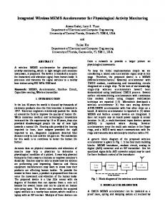
illumination Long Free Working Distance Interferometry reference In most interferometric microscopes, an arm incoherent source with a coherence length of ~10 µm is used for illumination. The key requirement for incoherent source interferometry is that the optical beam splitter path lengths from the beam splitter to the reference objective surface and to the sample must be the same to within (a) a few microns. This is usually achieved by placing the beam splitter and reference surface under the microscope objective in either a Michelson or Mirau realization, and comes at the expense of free working distance. In work to show the feasibility of the IMaP approach [4-11], we used a Michelson attachment that had a 5 mm free working distance. Test structures were actuated on individual chips with 3 1 inch free mm high electrical probes. As explained above, it is working preferable to use commercially available electrical distance probes at the wafer scale. One method to gain the (b) full free working distance of an objective is to use a second objective matched to the first, i.e., the Linnik interferometer. However, long working distance objectives required for wafer scale probing were not suitably matched for this approach to be effective. If the illumination is replaced by a coherent source, the path length requirement is alleviated. In Fig. 2(a), a beam splitter behind the objective is used (c) for the reference wave, and the optical path lengths to FIG. 2(a)—Modified the sample and to the reference surface are quite microscope on probe station, different. The illumination source is a 532 nm (green (b) closeup of objective with light) diode pumped, frequency-doubled Nd:YAG laser, with a coherence length of greater than 100 m. 2.5 cm free working distance, (c) interferogram of Green light is chosen because polysilicon has low cantilever beam array. transmission at this wavelength, and because objective aberrations are minimized at the center of the visible spectrum. As seen in Fig. 2(b), the full free working distance of the original microscope objective (~2.5 cm) is maintained, and off-the-shelf probes fit underneath easily. A good quality inteferometric image of cantilever beam test structures as captured by a CCD camera is shown in Fig. 2(c). Vibration has been reduced by placing the unit on an isolation table. Because the reference surface is mounted on a voltage-controlled piezoelectric crystal, its z-height is finely controlled. Details of the implementation will be published elsewhere. This design realization has numerous advantages over incoherent light interferometry. First, it is possible to obtain interferometry using different microscope objectives with only minor adjustment of the reference surface. Although 5X and 10X
TESTING MEMS MECHANICAL PROPERTIES
5
objectives were used in this work, good quality images of small structures have been obtained with a 50X objective at 1.3 cm free working distance. Also, the microscope has an internal zoom, producing a continuously adjustable magnification range of greater than 20 without changing objectives. Second, it is possible to image through a glass window in this implementation, important for applications where the device is in vacuum or in a sealed package. Third, besides monitoring simple test structures as in this work, this capability will also be very useful for three-dimensional imaging of full-scale micromachined devices at the wafer level. Fourth, the illumination is very bright, which is advantageous in high frame rate or stroboscopic applications. Algorithm and Software to Determine Cantilever Properties To test the effectiveness of the new system, we measured cantilever and fixedfixed beam properties along a column of a wafer. In Fig. 3, a step-by-step procedure to determine properties is shown, and in Fig. 4 the cantilever and its non-idealities are schematically represented. According to Step 1 of Fig. 3, thickness of the polysilicon layers was measured using a mechanical profilometer, and gap height g was measured by interferometry on cantilevers actuated into contact with the substrate (both to ~20 nm accuracy). The algorithm in Fig. 3 to determine cantilever properties has been detailed [6] and along with software enhancements is briefly described next.
R=1/κ
Step 1 -Measure t, g
+Vpad
Step 2 – Interferometer Measurement
θo
t
z(x, V pad =0V), unloaded beam
g Step 3 - Unloaded beam analysis Determine θo, κ
(a) Step 4 – Interferometer Measurement Measure z(x, V pad >0V), loaded beam
Step 5 - Initial analysis
Repeat at several voltages V pad < V pi
M
θ= θ0 + β M
( V pi -pull-in voltage)
Determine θ, E
Step 6 - Refined analysis Regression model for β, extract E
FIG. 3—Step-by-step procedure to determine cantilever
(b) FIG. 4(a)—Cantilever parameters t, g, θo and R=1/κ, (b) support post model.
6
MECHANICAL PROPERTIES OF STRUCTURAL FILMS
Three programs as portrayed in Fig. 5 were written to extract mechanical properties from deflection data (Steps 2-6 of Fig. 3). Interferograms of unloaded beams are recorded using an image analyzer program called “LineProfile Tool” per Steps 2 and 4 of Fig. 3. Within this program, reference points that indicate the beginning and end of the beam and where the linescan begins and ends are superposed on the image. The linescan (right side of Fig. 5), which contains fringe information as a function of pixel position, is stored in a file for further processing by a program called “Deflection Calculator.” This program converts the linescan information into pixel by pixel z-deflection data with near nm resolution, and also converts pixel data into x-position data. Software Program
Operation Performed
Computer Output beam begin
LineProfile Tool
beam end
1st pixel
last pixel
Select Beam, Apply Voltages, Output Linescan
Calculate Deflections
linescan (arb. units)
Deflection Calculator
z deflection (nm)
0
-400
-800
-1200
-1600 0
50
100
BeamPROPS Unloaded Cant. : θo, κ Loaded Cant. : β, E Fixed-fixed beam : σR
z deflection (nm)
Determine Property
150
200
250
pixel number
0 0
data model 0
-1000
V (volts) 0 30 40 -2000 50 60
E (GPa) -170.3 162.0 159.6 158.5
60
increasing V -3000 0
100
200
300
400
x position (um)
FIG. 5—Overview of algorithms to determine properties of beams. See text for discussion.
A program called “BeamPROPS” operates on the deflection data to extract properties in Steps 3, 5, and 6 of Fig. 3. BeamPROPS calculates model deflections by the finite difference method. For unloaded beams, it accounts for the non-idealities θ o and κ, and for the small effect of gravity. It determines the properties using a quasi-Newton search algorithm by adjusting the model until the error between the data and the model deflections are minimized. Model fits to deflections of unloaded cantilevers along a wafer column are shown in Fig. 6. These deflections are well described by the equation
TESTING MEMS MECHANICAL PROPERTIES
7
0 -0.5
z deflection (µ µ m)
7 -1
4 1 in 10 data points shown
-1.5
5 6
8
3
-2 model fit
-2.5
row #
-3
1 2
-3.5 0
200
400
x
(µ µ m) pos
600
800
FIG. 6—Deflection profiles of unloaded cantilevers along a wafer column. x2 z ( x) = θ o x + κ , (1) 2 where z (x) is positive for deflections away from the substrate. Typical root mean square (rms) errors between the data and the model are ~2 nm/pixel. The resolution for θ o is approximately 50 µrad, while for κ it is approximately 1 m-1, corresponding to ~0.15 MPa/µm stress gradient resolution (note that stress gradient = Eκ). Once θ o and κ are known for a given cantilever, a similar analysis procedure is performed by BeamPROPS on electrostatically loaded beams (Fig. 4(a)) to find loaded beam takeoff angle θ and E per step 5 of Fig. 3. Electrostatic loading with a fringing field correction is incorporated in the finite difference model calculations. The quasi-Newton search algorithm travels through (θ, E) space to rapidly find an optimum fit to the measured data, typically within five seconds. For a given cantilever, values of θ and E are found at each voltage loading. Non-systematic errors affect these values. Therefore, the slope in a regression model in which θ is plotted against the best fit calculated moment M is used to determine a value for support post compliance β , according to the equation (2) θ = θ o + β M, as shown in Fig 4(b). Using the value for β , the deflection data is re-analyzed by BeamPROPS to determine the best values for E per step 6 of Fig. 3. An example of the optimum fit to the measured data and the associated values for E are shown in the bottom right hand corner of Fig. 5. Note that at larger voltages, where E exerts its maximum effect on flexures, the values of E are repeatable. An actuation pad of 180 µm length near the support post was used to apply the voltages according to the principle of leveraged bending [15], and cantilevers analyzed were 300 to 700 µm in length. In the wafer column data below, values of E at each die site are averaged for several voltage loadings and several beams. To determine residual stress (due to average residual stress through the thickness of the film), the deflection profiles of unloaded fixed-fixed beams of 1000 µm length were measured and found to be well represented by a sinusoidal shape, indicating that the beams were buckled in compression. Residual stress σ R was calculated from the Euler buckling result π 2 3 A 2 + 4 t 2 , (3) σ R = −E 12 L2
MECHANICAL PROPERTIES OF STRUCTURAL FILMS
8
where L is the length of the fixed-fixed beam and A is the buckled beam amplitude, and the minus sign is for compression. Equation 3 assumes that the beam is well into the post-buckling regime, which is very reasonable for these long beams. The effect of stress gradient on the calculated result is small, and the resolution of the measurement with respect to σ R is approximately 1 MPa. A value of E = 161 GPa was assumed in the calculations. Here, only unloaded beams were analyzed. However, we have demonstrated that by applying voltages to fixed-fixed beams, independent confirmation of σ R can be obtained [16].
row 1 column tested 15 cm
(a)
8 7 g (um)
µm) t (µ
6
(b)
6
5
5
4
4
3
3
t (um)
2
2
1
1
0
0 5
-500 θ (µ µrad) (T1) 0
-750
0 -1
κ (m )
-1000
θ0 (µ µrad)
µm) g (µ
7
-1250
κ (mm (m-1))-1) ρ -1
-5
-1500 -1750
-10
180
6 Avg. E (GPa) (T3)
160
5
140
4
β (µ µrad/µ µN*µ µm))
120
3
100
2
80
1
(d)
σR (MPa)
0
-5
FIG. 7—Column map for materials properties (a) wafer, (b) t, g, (c) θo, κ, (d) E, β, (e) σR.
-10
-15
(e)
β (µ µrad/µ µN*µ µm)
Avg. E (GPa)
(c) -2000
Results and Discussion Diagnostic test structures were laid out and included on each die site along with MEMS devices. A lot was fabricated according to our standard MEMS process flow [1], in which four independent structural layers of polysilicon are produced. After processing, structures were freed by a standard “release” process. The wafer was then loaded onto the testbed described above. Wafer alignment was accomplished by manual operation of the chuck motor, voltages were manually programmed, and the three software tools listed above were run sequentially. Work is in progress to seamlessly integrate the three programs with automatic operation of the chuck. Figure 7 shows testing results of mechanical properties along a column of die sites as represented in Fig. 7(a) for the third level of polysilicon, “Poly 3”. Figure 7(b) shows tight control of thickness, with t = 2.34 +/- 0.02 µm. Poly 3 gap height g is not as well controlled as thickness, with values from 5.53 to 6.03 µm. This variation across the wafer is reasonable given the chemical mechanical polishing (CMP) process of the oxide layer underlying Poly 3. It is important to measure the geometrical properties t and g accurately (to ~20 nm) on each individual device, because the subsequent analysis to determine E depends strongly on these values.
0
1
2
3
4
row
5
6
7
8
9
TESTING MEMS MECHANICAL PROPERTIES
9
The values of unloaded cantilever takeoff angle θ o and curvature κ , reflecting the data of Fig. 6, are shown in Fig. 7(c). It is seen that θ o is negative but relatively constant across the wafer, with values of –750 to –1000 µradians. We attribute the negative values of θ o to oxide incorporation within the support post structure [6]. After release, the highly compressive deposited oxide is no longer constrained, and we believe this induces the support to pivot (we have subsequently reduced θ o by an improved support post design). Typical values in Fig. 7(c) of κ from -1 to -2.5 m-1 (corresponding to stress gradient values of –0.16 to -0.4 MPa/µm) are quite low for MEMS devices. Note in Row 1 that θ o drops sharply to –1500 µrad and also that κ decreases significantly to –10 m-1. The change in κ may be due to a subtle microstructural feature [17] or trace contaminant such as the oxygen level [18] being different in the Poly 3 layer at this die location relative to the rest of the wafer (other sources are also possible, and this is a subject for future research). This in turn may be responsible for the sharp drop in θ o . Clearly, both negative θ o and negative κ are undesirable for MEMS devices, which often contain long structural elements assumed to be flat over the substrate. In Fig. 7(d), the values of E are seen to be relatively constant across the substrate. This is expected because it is unlikely that the subtle changes in stress gradient at the sub MPa/µm level (or the changes in σ R at