Integrated standing-wave transform spectrometer for near infrared optical analysis. S. R. Bhalotra, H. L. Kung, J. Fu, N. C. Helman, O. Levi, D. A. B. Miller, and ...
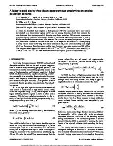
Integrated standing-wave transform spectrometer for near infrared optical analysis S. R. Bhalotra, H. L. Kung, J. Fu, N. C. Helman, O. Levi, D. A. B. Miller, and J. S. Harris, Jr. Edward L. Ginzton Laboratory and Solid State Photonics Laboratory Stanford University, Stanford, CA 94305-4085 A novel, compact standing-wave Fourier-transform spectrometer design has been developed for applications in the near IR. Whereas recent development of the standing-wave architecture has been focused on interferometric sensing [1] and spectrometry [2, 3] in the visible domain using Si detectors, we demonstrate spectral analysis from 633 nm to 866 nm. The spectrometer is composed of a GaAs p-i-n photodetector with 550 Å active region integrated with a Si MEMS scanning electrostatic mirror-actuator. The device has an equilibrium mirror-detector spacing of 17 µm and a total volume of only 0.2 cm3. The integrated system provides permanent optical alignment and simple lowpower operation. This spectrometer could be useful in a variety of applications including on-site biochemical analysis and mobile sensing systems. Mirror Frame
Pillar
Flexure
13 mm 13 mm
Photodetector
Detector Holder
17 mm
Fig. 1. Left: spectrometer schematic. Light enters from below the detector holder, traverses the photodetector, and reflects off the mirror pillar back toward the detector. Right: photos of mirror and detector holder.
This miniature spectrometer is based on the 1-D standing-wave transform spectrometer architecture [2] with a parallel-plate MEMS mirror and a partially transmitting photodetector. Incident light reflecting off the mirror creates an optical standing wave. While the mirror scans along the optical beam axis, the detector samples the moving standing wave; the Fourier transform of the resulting time-varying photocurrent yields the optical spectrum. This spectrometer architecture offers the same advantages as other Fourier transform spectrometers, such as throughput and multiplexing, but in an optically 1-D system. The partially transmitting photodetector removes the need for a beamsplitter and
second optical arm, minimizing the number of required optical components. The 17 x 13 × 1 mm device is shown in Fig. 1. Spectrometer resolution improves with total mirror scan length, so the parallel-plate Si MEMS mirror was designed for large displacement when driven at its resonance frequency. A bulk Si micromachining process was developed to provide a uniform flexure thickness. First a 2 µm boron-doped Si etchstop was grown epitaxially on a 4” double-side-polished Si wafer. The etchstop was then removed by plasma dry etching everywhere except the mirror pillar, flexure, and frame areas. After an oxide preparation, 16 µm of single crystal intrinsic Si was epitaxially grown on the flexures. A nitride film was deposited on both sides and patterned on the back side to protect the mirror frame and pillar. The unprotected material, except the boron-defined flexures, was then etched in potassium hydroxide. In this way the flexure thickness is determined by the epitaxially grown Si layers. After nitride removal, the wafer was coated on both sides with Au, providing high reflectivity in the near infrared and high electrical conductivity for the actuator drive signal. The mirror is actuated by applying a voltage between the back of the mirror pillar and a parallel ground reference. Driven with a DC-offset sinusoid with Vpp = 100 V on-resonance at 830 Hz, the mirror moves almost perfectly harmonically and symmetrically around its equilibrium position with a total scan length of 17.8 µm. The high scan rate enables fast, continuous spectral analysis. Flexure uniformity allows the mirror to remain perpendicular to the optical beam as it scans along the beam axis, preventing beam walkoff. The photodetector, mounted in front of the mirror, must transmit a significant fraction of the input light to allow a standing wave of sufficient amplitude. The detector is a GaAs/AlGaAs p-i-n diode grown by molecular beam epitaxy on a GaAs substrate. The GaAs intrinsic region, which samples the standing wave, has a thickness of 550 Å to maximize interferogram fringe visibility [2] for λ~ 800 nm. On either side of the GaAs layer is 500 Å of intrinsic Al0.3Ga0.7As, which is nominally transparent above 687 nm. These regions increase the diode breakdown voltage and provide a buffer to prevent dopant diffusion into the active GaAs layer. The p- and n- regions are 0.25 µm and 0.5 µm, respectively, of heavily doped Al0.3Ga0.7As. The p-i-n diode was
grown on a 0.2 µm Al0.85Ga0.15As etchstop. The mesa area and n-area were defined by plasma dry etching, and coplanar ohmic ring contacts were made to the p- and n-layers by evaporation of Ti/Au and Ge/Au/Ge/Au/Ni/Au, respectively. We chose a detector with 1 mm x 1 mm active area for easy alignment; the total detector size is 2 mm x 2 mm x 1.1 µm after substrate removal. The detector was flip-chip bonded to a 17 mm x 13 mm quartz detector holder. The center of the holder was recessed 17 µm by etching in a HF bath to accommodate mirror motion toward the detector. Au electrical traces were evaporated onto the surface for photocurrent extraction. Au-Au bonds provide electrical connections between the detector ring contacts and the traces on the holder. Transparent epoxy was added for mechanical stability. The GaAs substrate was removed down to the AlGaAs etchstop using a selective citric acid / hydrogen peroxide etch. Finally, excess epoxy was removed by plasma dry etching. For detectors of this type, dark currents as low as 0.5 nA were measured for a reverse bias of 0.5 V. The single-pass responsivity at 810 nm was 33 mA/W. The detector package and mirror were aligned and integrated with a thin adhesive layer of photoresist. Electrical leads were soldered onto the two detector electrodes and the mirror outer frame. The detector nregion is used as the ground reference for the scanning mirror. The n-region is a 2 mm x 2 mm area that matches the mirror surface area. The capacitance of this parallel-plate system is only 4.2 pF; thus power consumption is low. This packaging guarantees positional and angular alignment of the detector with the moving mirror reflective surface. A key element of this design is that it allows the scanning mirror to approach within a few µm of the detector, which enables measurement of interferograms from sources with low spectral coherence (lacking narrowband spectral features). An optical beam with 40 nm bandwidth around 750 nm has a coherence length of 14 µm; our design allows the mirror to move within 7 µm (half the coherence length) of the detector, where the interferogram amplitude is relatively large. This should enable detection of a wide range of low coherence radiation, including visible-IR LEDs and fluorescence emission in biochemical samples. The device was tested with two laser sources: a 6.25 mW HeNe laser at 633 nm and a 2.30 mW external cavity diode laser at 866 nm. Interferograms were sampled and transferred to a computer, where the ‘current vs. time’curves were mapped to ‘current vs. mirror displacement’ curves, accounting for the sinusoidal mirror motion. Discrete Fourier transforms yield optical spectra, superimposed in Fig. 2. Though the AlGaAs layers absorb ~ 90% of the input intensity at
633 nm and the interferogram amplitude is diminished, an interferogram is still measurable with increased optical power. The full widths at half maximum are 574 cm-1 (23 nm) for the 633 nm peak and 707 cm-1 (53 nm) for the 866 nm peak.
Fig. 2. Superimposed spectra from lasers at 866 nm and 633 nm, demonstrating a spectral range into the near IR.
In conclusion, we have presented an integrated standing-wave spectrometer operating in the near IR. Mirror flexure uniformity allows for increased mirror scan length without tip-tilt problems, which improves spectral resolution. The GaAs detector provides excellent near IR responsivity. The integrated design allows the mirror to move within a few µm of the detector. The simple operation of this compact device, with a lowpower continuous-scan mirror, permanent alignment, and only three contacts, should enable implementation in a wide variety of miniaturized sensing systems. This work was supported by the U.S. Air Force under contract No. F49620-00-C-0040 and by the Defense Advanced Research Projects Agency under a grant for Photonic Wavelength And Spatial Signal Processing and contract No. MDA972-98-1-0002, a sub-award from Univ. New Mexico. SRB and NCH gratefully acknowledge the support of the Regina and Gerhard Casper Stanford Graduate Fellowships. [1] M. Sasaki, X. Mi, K. Hane, “Standing wave detection and interferometer application using a photodiode thinner than optical wavelength,” App. Phys. Lett. (1999). [2] H. L. Kung, S. R. Bhalotra, J. D. Mansell, D. A. B. Miller, and J. S. Harris, Jr., "Standing-wave transform spectrometer based on integrated MEMS mirror and thin-film photodetector," IEEE J. Selected Topics in Quantum Electronics (2002). [3] D. Knipp, H. Stiebig, H. J. Buechner, M. A. Rosa, R. A. Street, “Design and modelling of a Fourier spectrometer based on sampling a standing wave,” Proc. Material Research Society (2001).