Processing and Application of Ceramics 3 [4] (2009) 187–190
Investigation of electrical properties of vacuum annealed titanium oxide containing ceramics# Agnese Pavlova1,*, Janis Barloti2, Valdis Teters2, Janis Locs1, Liga Berzina-Cimdina1 Riga Technical University, Riga Biomaterials Innovation and Development Centre, Pulka Street 3/3, Riga, LV-1007, Latvia 2 Riga Technical University, Division of Electronic Equipment, Latvia 1
Received 16 September 2009; received in revised form 24 November 2009; accepted 22 December 2009
Abstract Titanium oxide ceramics were prepared using extrusion process and subsequent thermal treatment in two stages – in air atmosphere at 1150°C and than in vacuum at temperatures between 1200 and 1350°C. Influence of thermal treatment conditions on microstructure and electrical properties (thermopower, conductivity of semiconductor and electron activation energy) of obtained ceramics was investigated. It was confirmed that all samples treated in vacuum are n-type semiconductors. It was also found that the increase of temperature during sintering in vacuum leads to increased electrical conductivity, however, the highest thermopower values were obtained for samples thermally treated in vacuum at 1225°C. Electron activation energy (ΔE), calculated using dependence of conductivity of samples on temperature, was is in the range from 0.049 to 0.061 eV. The obtained products can be used as electrodes for water treatment technology based on photoelectrolysis. Keywords: titanium oxide, vacuum sintering, microstructure, electrical properties I. Introduction There are many innovative technologies based on TiO2 applications such as photoelectrochemical cells, photocatalytic treatment of organic waste and electrochemical sensors [1–6]. Among many semiconductors employed TiO2 is known to be a good photocatalyst. TiO2 has high photosensitivity and strong oxidizing power, it is non-toxic, easily available and has a long-term stability [7,8]. High attention is paid to water pollution and its treatment. Electrolysis and many other methods have been adopted to reduce the pollution. Conductive titanium oxide ceramics can be used for microbiologically contaminated water purification [9]. It is well known that titanium oxide ceramics have good biocompatibility and hemocompatibility [10,11]. Rutile is thermodynamically the most stable of the three crystal TiO2 modifications. Rutile has a smaller band gap (3.0 eV) compared to anatase (3.2 eV) and therefore is chemically more stable [12,13]. Titanium oxide can form nonstoichiometric Paper presented at 8th Students’ Meeting, SM-2009, Processing and Application of Ceramics, Novi Sad, Serbia, 2009 * Corresponding author: tel: +371 670 89 605 fax: +371 670 89 619, e-mail:
[email protected] #
compounds, which have different electrical properties than stoichiometric titanium oxide. Titanium oxide with the common formula TinO2n-1 (where n is a number from 4 to 10), or Magnelli phases, are compounds which have additional electron level in band gap and exhibit semiconducting properties [14]. Electron level position in the band gap and electron activation energy (energy necessary to move an electron from the valence zone to the conductivity zone or from the valence zone to free electron levels in the band gap) of obtained titanium oxide ceramics depend on the processing conditions (especially thermal treatment conditions). Electrical properties of titanium oxide are sensitive to the oxygen partial pressure, since it changes the concentration of electrons or electron holes in the oxides. Owing to the fact that the porosity within the oxides may alter their inside oxygen partial pressure, the porosity in a semiconducting oxide could affect its electrical properties [15]. In addition, grain boundary is another major microstructural feature in a semiconducting oxide. This is because grain boundary may absorb charge carriers and in turn repel the same charge carriers travelling to the boundary as part of the conduction process. In some cases a second phase may
187
A. Pavlova et al. / Processing and Application of Ceramics 3 [4] (2009) 187–190
precipitate along grain boundaries to become a barrier for electrical conduction. Thermal treatment of titanium oxide ceramics in vacuum atmosphere at different temperatures changes not only electrical properties but also microstructure of the material. The aim of this study is to investigate microstructure and electrical properties of titanium oxide ceramics prepared using extrusion process and subsequent thermal treatment in air at 1150°C and than in vacuum at different temperatures. The obtained products can be used as electrodes for water treatment technology based on photoelectrolysis. In comparison with currently widely used Pt, PbO2, Ti/SnO2 with Sb2O5 impurities, IrO2, PtIr, RuO2, MnO2, Ti/diamond with boron impurities, as well as graphite electrodes, titanium dioxide has good chemical stability, high resistance to corrosion, but much lower production cost [16].
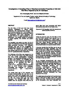
II. Experimental Sample preparation Titanium oxide samples were prepared using industrial scale extruder. Extrusion mass consisted of anatase 75 wt.% (TiO2, Hombitan, Sachtleben Chemie GmbH), water 22 wt.%, lubricant 3 wt.% (PRODUKT KP 5144) and binder 2 wt% (ZUSOPLAST C 93, Zschimmer & Schwarz GmbH & Co KG). The obtained green bodies (Ø 10 mm) were heated at 1150°C with 5 °C/min heating rate and 2 h dwell time to burn out the additives and obtain rutile crystallographic modification. Further, samples were treated in vacuum (6.6·10-3 Pa) at different temperatures between 1200 and 1350°C with 7 °C/ min heating rate and 1 h dwell time. After sintering the samples were cut into 20 mm long rods. Ends of the samples were polished with SiC paper in the sequence of 280, 1500, 2000 grit and cleaned with ethanol. Sample surface was cleaned using vacuum sparking discharge. For better electrode-material contact a thin aluminium film (0.2–0.3 μm) was deposited on the ends of the samples using vapour deposition technique. Crystalline phases in the samples were identified using X-ray diffraction (XRD) (PANalytical X’Pert Pro). Cu Kα filtred radiation over 2θ range from 20° to 85° was used. Microstructure of the sample fracture surface was investigated using FE-SEM (Mira / LMU, Tescan). Electrical properties measurement Custom made equipment (Fig. 1) was used for measurement of electrical properties. To decrease the surface conductivity of the samples and heat loss, measurements were carried out in vacuum (2.6 Pa). With this equipment the dependence of thermopower and the resistance on temperature can be measured and also simultaneously conductivity type can be determined. Electrical conductivity was calculated from resistance of the material. Temperature gradient was measured by thermocouples mounted in the copper electrodes, attached to the end of the samples. For
the thermopower measurements of the samples and thermocouples, direct current potentiometers were used. The thermal effect of thermal probe is used for determination of electrical conductivity of a semiconductor [17]. The method is based on Tompson effect in semiconductor, and it can be described as follows, supposing that an n-type semiconductor is measured. If one end of the sample is heated, the heat input will generate electrons and holes. Since it is assumed that the semiconductor is n-type, the electron concentration will be greater than the hole concentration. Electrons will move from hot to cold end of the sample, where after some time the electron concentration will be higher. Consequently, the n-type semiconductor cold end will be charged negative, but the hot end will be positive. Using this method semiconductor conductivity type can be determined. Magneto’s electrical system voltmeter was used for determination of polarity. In turn the graphical method for calculation of electron activation energy was used (this is a widespread method in of semiconductor physics).
Figure 1. Schematic view of equipment used for the electrical measurements
III. Results and discussion Density of samples was determined using Archimedes method and was found to be in range from 3.32 to 3.64 g/cm3. Water uptake was 3 to 4 % and total porosity 10 to 14%. The crystalline structure of the prepared titanium oxide samples was examined using XRD (Fig. 2). The main diffraction pattern has characteristic peaks for
188
Figure 2. X-ray diffraction pattern of obtained samples
A. Pavlova et al. / Processing and Application of Ceramics 3 [4] (2009) 187–190
a)
b)
c)
d)
1200°C
1350°C
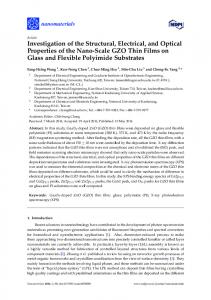
Figure 3. SEM microphotographs of titanium oxide ceramics treated in vacuum at 1200°C (a) middle and (b) edge of sample, and at 1350°C (c) middle and (d) edge of sample
TiO2 rutile phase. However, a few very weak peaks are visible too, which could be indication for presence of some nonstoichiometric titanium dioxide phases. SEM micrographs of titanium oxide samples treated in vacuum at different temperatures are shown in Fig. 3. The microstructure of sample treated at 1200°C differs between the middle and the edge of the sample. In the middle of the sample grains are larger than on the edge of the sample. Increasing the treatment temperature induces densification and grain growth. Thus, grain size reaches 30 μm at 1350°C compared to 10 μm at 1200°C. It was also observed that the middle of all samples was more porous than the edge of the samples. Such density (and grain size) difference could occur because of the used extrusion forming technology. Thermopower measurements were made in negative temperature range down to –180°C by cooling with liquid nitrogen (LN2) and in positive range up to +400°C by thermoresistive heating (Fig. 4). At equal temperature gradients in all measured temperature range the samples sintered in vacuum at 1225°C had the highest thermopower. It confirms that thermal treatment conditions are very important for electrical properties of titanium oxide ceramics.
Conductivity was calculated from the resistance. It was found that increase of temperature during sintering in vacuum leads to increased electrical conductivity (from 15 to 55 Ω-1·m-1). In semiconductor physics, the higher thermopower value does not provide the best conductivity in semiconductor materials. This is probably due to the electric conductivity along grain bound-
189
Figure 4. Relation between thermopower and temperature difference between the ends of the sample (ΔT) for samples thermal treated in vacuum at 1200°C, 1225°C and 1300°C: a) LN2 cooled and b) heated
A. Pavlova et al. / Processing and Application of Ceramics 3 [4] (2009) 187–190
aries, since at higher temperatures the largest grains are created, decreasing grain border surface area. The obtained results also shown that the samples sintered in air have no semiconducting properties, whereas all samples treated in vacuum are n-type semiconductors. Electron activation energy (ΔE), calculated using dependence of conductivity of samples on temperature, was is in the range from 0.049 to 0.061 eV.
IV. Conclusions Titanium oxide ceramics were prepared using extrusion process and subsequent thermal treatment in air at 1150°C and than in vacuum at different temperatures upto 1350°C. It was confirmed that the samples sintered in air have no semiconducting properties, whereas all samples treated in vacuum are n-type semiconductors. The increase of temperature during sintering in vacuum leads to increased electrical conductivity, however, the highest thermopower values were obtained for samples thermally treated in vacuum at 1225°C. Electron activation energy was is in the range from 0.049 to 0.061 eV. All these confirm that thermal treatment conditions are very important for electrical properties of titanium oxide ceramics. Acknowledgment: This work has been partly supported by the European Social Fund within the National Program “Support for carrying out doctoral study programs and post-doctoral researches” project “Support for the development of doctoral studies at the Riga Technical University”.
References 1. M. Redecka, M. Rekas, “Charge and mass transport in ceramic TiO2”, J. Eur. Ceram. Soc., 22 [12] (2002) 2001–2012. 2. M. Radecka, M. Rekas, A. Trenczek-Zajac, K. Zakrzewska, “Importance of the band gap energy and flat band potential for application of modified TiO2 photoanodes in water photolysis”, J. Power Sources, 181 [1] (2008) 46–55. 3. M.A. Afifi, M.M. Abdel-Aziz, I.S. Yahia, M. Fadel, L.A. Wahab, “Transport properties of polycrystalline TiO2 and Ti2O3 as semiconducting oxides”, J. Alloys Compd., 455 [1-2] (2008) 92–97. 4. S.K. Mohapatra, M. Misra, V.K. Mahajan, K.S. Raja, “A novel method for the synthesis of titania nanotubes using sonoelectrochemical method and its application for photoelectrochemical splitting of water”, J. Catal., 246 [2] (2007) 362–369.
5. J. Hu, H. Qin, Z. Sui, H. Lu, “Characteristic of mechanically milled TiO2 powders”, Mater. Lett., 53 [6] (2002) 421–424. 6. T. Bak, T. Burg, S.-J.L. Kang, J. Nowotny, M. Rekas, L. Sheppard, C.C. Sorrell, E.R. Vance, Y. Yoshida, M. Yamawaki, “Charge transport in polycrystalline titanium dioxide”, J. Phys. Chem. Solids, 64 [7] (2003) 1089–1095. 7. J.R. Smith, F.C. Walsh, “Electrodes based on Magneli phase titanium oxides: the properties and application of Ebonex® materials”, J. Appl. Electrochem., 28 (1998) 1021–1033. 8. N. Venkatachalam, M. Palanichamy, V. Murugesan, “Sol-gel preparation and characterization of nanosize TiO2: Its photocatalytic performance”, Mater. Chem. Phys., 104 [2-3] (2007) 454–459. 9. N. Wetchakun, S. Phanichphant, “Effect of temperature on the degree of anatase-rutile transformation in titanium dioxide nanoparticles synthesized by the modified sol-gel method”, Curr. Appl. Phys., 8 [3-4] (2008) 343–346. 10. J. Chen, M. Liu, L. Zhang, J. Zhang, L. Jin, “Application of nano TiO2 towards polluted water treatment combined with electro-photochemical method”, Water Res., 37 [16] (2003) 3815–3820. 11. A.G. Mantzila, M.I. Prodromidis, “Development and study of anodic Ti/TiO2 electrodes and their potential use as impedimetric immunosensors”, Electrochim. Acta, 51 [17] (2006) 3537–3542. 12. M. Nag, P. Basak, S.V. Manorama, “Low-temperature hydrothermal synthesis of phase-pure rutile titania nanocrystals: Time temperature tuning of morphology and photocatalyst activity”, Mater. Res. Bull., 42 [9] (2007) 1691–1704. 13. J. Manriquez, L.A. Godinez, “Tuning the structural, electrical and optical properties of Ti (III)-doped nanocrystalline TiO2 films by electrophoretic deposition time”, Thin Solid Films, 515 [7-8] (2007) 3402– 3413. 14. M. Radecka, A. Tranczek-Zajac, K. Zakrzewska, M. Rekas, “Effect of oxygen nonstiochiometry on photo-electrochemical properties of TiO2-x”, J. Power Source, 173 [2] (2007) 816–821. 15. S.H. Song, X. Wang, P. Xiao, “Effect of microstructural features on the electrical properties of TiO2”, Mater. Sci. Eng., 94 [1] (2002) 40–47. 16. X. Chen, F. Gao, G. Chen. “Comparison of Ti/BDD and Ti/SnO2–Sb2O5 electrodes for pollutant oxidation”, J. Appl. Electrochem., 35 [2] (2005) 185–191. 17. K. Seeger, Semiconductor Physics, Springer, Berlin 2004.
190