Magnetic fingerprint in a ferromagnetic wire: Spin torque diode ... which is a consequence of the spin angular momentum transfer occurring the interaction.
Magnetic fingerprint in a ferromagnetic wire: Spin torque diode effect and induction of the DC voltage spectrum inherent in the wire under application for RF current
A. Yamaguchi1, T. Ono2, Y. Suzuki3, S. Yuasa4, and H. Miyajima1
1
Department of Physics, Faculty of Science and Technology, Keio University, 3-14-1 Hiyoshi,
Yokohama, Kanagawa 223-8522, Japan
2
Institute for Chemical Research, Kyoto University, Gokasho, Uji, Kyoto 611-0011, Japan
3
Graduate School of Engineering and Science, Osaka University, Machikaneyama 1-3,
Toyonaka, Osaka 560-8531, Japan
4
Nanoelectronics Research Institute, National Institute of Advanced Industrial Science and
Technology, Tsukuba 305-8568, Japan
1/1
[Abstract] We report the rectifying effect of a constant-wave radio frequency (RF) current by a magnetic
domain wall (DW) on a single-layered ferromagnetic wire. A direct-current (DC) voltage is
generated by the spin torque diode effect, which is a consequence of magnetoresistance
oscillation due to the resonant spin wave excitation induced by the spin-polarized RF current.
The DC voltage spectrum strongly depends on the internal spin structure in the DW, which
corresponds to the magnetic fingerprint of the spin structure in the ferromagnetic wire.
2/2
A magnetic domain wall (DW) is the magnetization spatial transition region between magnetic
domains, in which the magnetic moments undergo reorientation. Most of the magnetic changes
under the action of weak and moderate magnetic fields occur at DWs and understanding of DW
behavior is hence one of the essentials in describing the magnetizing process. There are many
studies on planer displacement of rigid DWs under the action of the magnetic field [1 – 3] and
electrical current [4 – 13]. In general, the DW is subjected to magnetic potential energy in a
ferromagnet. The potential energy varies throughout the ferromagnet since some defects
existing in the material provide minima of the potential energy, while the region of
inhomogeneous microstress, associated with dislocations, provides either energy minima or
maxima depending on the sign of the stress and magnetostriction coefficient [1 – 3]. The
fingerprint appropriate for the random potential in magnetic materials has been studied from the
viewpoint of the Barkhausen effect in Fe-Ni-Co alloy [14] and from the magnetic field
dependence of conductivity fluctuations in a variety of mesoscopic systems [15, 16, 17].
Recently, Vila et al. have reported that DWs make a reproducible spin contribution to the
universal conductance fluctuation and that they also lead to hysteric behavior with
irreproducible fluctuations observed in the minor loop [17]. The shape of the potential is
3/3
irregular in the space and acts on the internal spin structure of the DW in the absence of a
magnetic field.
When a spin-polarized electrical current flows through some spin structure with
variation such as ferromagnetic multilayers [18 – 21], the DW [4 – 9], or a magnetic vortex [22],
magnetization switching and magnetic excitation are induced by the spin-transfer effect [23, 24],
which is a consequence of the spin angular momentum transfer occurring the interaction
between the spin-polarized current and the magnetic moment. One of the interesting properties
is the spin-torque diode effect found in the magnetic tunnel junction (MTJ) [24], the spin-valve
giant magnetoresistive device (SV-GMR) [25], and single-layered ferromagnetic wires [27]. It
should be noted that direct-current (DC) voltage is produced when a radio-frequency (RF)
current flows through a nanometer-scale MTJ, a SV-GMR, or a ferromagnetic submicron wire.
This DC voltage generation originates in the magnetoresistance oscillation due to the
ferromagnetic resonance (FMR) generated by the spin-transfer effects [25, 26]. As reported in a
previous paper [27], the spin torque diode effect in the single-layered ferromagnetic wire is the
consequence of the magnetoresistance oscillation generated by the spin-transfer torque. The
torque is a combined effect of the spatial non-uniformity of the magnetization and the flow of
4/4
the spin-polarized current.
In the other words, the spin torque diode effect is highly sensitive
to the spin structure in nano-scale magnets.
In this study, we present the spin torque diode effect in a single-layered ferromagnetic
wire without an external magnetic field. The DC voltage spectrum depends on the internal spin
structure at the DW, which corresponds to the magnetic fingerprint reflected by the variation of
the potential energy in the wire.
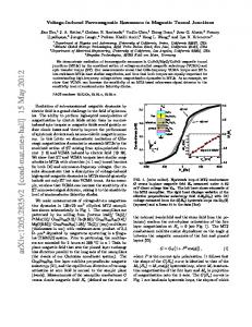
Two kinds of wire, boomerang-shaped and semicircular-shaped ferromagnetic wires of Ni81Fe19, were fabricated on MgO substrates using electron beam lithography and the liftoff method.
Figure 1(a) shows an optical micrograph of the boomerang-shaped wire and the present RF
electric circuit.
The size and shape of the wires prepared in this study are listed in Table 1.
The measurement system is almost same as that described in the previous paper [27]. A
microwave probe is connected by the wire, and the bias tee circuit detects the DC voltage
difference induced by the RF current flowing through the wire, as schematically illustrated in
Fig. 1 (a). A vector network analyzer (frequency range: 45 MHz – 67 GHz) or a signal generator
(frequency range: 10 MHz – 40 GHz) injects the RF current into the wires. All experiments are
performed at room temperature in the absence of an external magnetic field.
5/5
In the soft ferromagnetic Ni81Fe19 narrow wire, the magnetization is directed along the
wire axis owing to the presence of strong uniaxial shape anisotropy. Therefore, we are able to
introduce or remove a single DW in the following manner: A DW is introduced (removed) by D D applying a magnetic field, H=1 kOe, at an angle of θ = 90 ( θ = 0 ) so as to saturate the
magnetization and decrease the field to zero. The magnetic structures of the head-to-head DW
and no DW in the wire calculated by a micromagnetics simulator (OOMMF) [28] are shown in
Fig. 1 (b) and (c), respectively. The parameters used for the calculation are as follows: a unit cell size of 5 nm × 5 nm with a constant thickness of 50 nm, a magnetization of 1.08 T, and a damping constant of α = 0.1 . The size of the simulation model is same as sample SC1 apart
from the wire length.
The dynamical properties of the DW magnetization are probed using the vector
network analyzer in the microwave reflection mode. In order to remove the effect of cables, on-
wafer calibration is performed using the open-short-load calibration procedure [29]. We
calibrate reflection signal S11 of sample SC1 with the DW, and measure signal S11 after the DW
is removed in the previously described manner. In Fig. 1 (d), the red dashed line and the black
solid line correspond to S11 with and without a DW, respectively. The eigenmodes of the
magnetization in the wire with and without a DW are determined by free damping applying a
6/6
pulsed magnetic field along the z-direction (perpendicular to the plane). After this excitation,
the magnetization in the wire performs damped free oscillations. Figures 1(e) and 1(f) show the
time variation of the z-componet of the magnetization and the Fourier spectrum, respectively.
As shown in Fig. 1(f), the wire without a DW has an intrinsic frequency of 9 GHz, while the
wire with a DW takes a frequency of 1, 2, and 8 GHz. The frequency of the magnetization
oscillation in the wire with a DW is smaller than that in the wire without a DW. The dips in S11
of the wire without a DW at frequency of 9.5 and 10.4 GHz correspond to the magnetization
oscillation in the wire with and without a DW, respectively. The decrease in S11 of the wire
without a DW in the range lower than 5 GHz also corresponds to the magnetization oscillation
calculated in the wire with a DW.
Figure 2 shows the RF current frequency (RF power: -5 dBm) dependence of the DC
voltage difference due to the spin torque diode effect in the absence of a magnetic field. The
black dashed line and the red solid line correspond to the spectrum without a DW and with a
DW, respectively. As shown in Fig. 2, the observed resonance spectrum of the wire with a DW
is more complicated than that of the wire without a DW. This indicates that the complicated
resonance spectrum is a consequence of the spatial non-uniformity of the magnetization due to
the existence of a DW. In other words, the effective magnetic field is homogenous in the wire
7/7
without a DW, but the effective field depends on the position of the wire with a DW due to the
internal spin structure. The spatial inhomogeneity of the effective field produces the
complicated spectrum. That is, the spin torque diode signal shows a pattern inherent in each
wire, or a magnetic fingerprint, reflecting the spatial variation of the spin structure with high
sensitivity compared with S11 measurement. Figure 3 shows the RF power and frequency dependences of the induced DC voltage
difference for samples SC1 and SC2 with a DW. The amplitude of the DC voltage spectrum
increases with increasing RF current, but the spectrum structure is conserved. This indicates that
the spin-transfer torque or the Joule heating due to the RF current is not as large as the magnetic
spatial structure disarranged. That is, there is spectral reproducibility [14 – 17].
We repeated erasing the DW, introducing the DW again, and measuring the rectifying
effect of the RF current in the wire in the absence of an external magnetic field. The DC voltage
spectra of samples SC2 and SC3 are shown in Fig. 4 (a) and (b), respectively, in which the
number following the symbol # means the number of measurement times. As is seen in Fig. 4
(a), three kinds of spectrum are observed; the spectra for #2, #3, #4, and #6 are the same as each
other but different from those of #1 and #5, while the spectra for #1 and #6 are the same but
different from those of #2, #3, #4, and #5, as shown in Fig. 4 (b). After the DW is erased and
8/8
introduced, a small change in the spin configuration in the wire slightly modifies the magnetic
fingerprint of the DW. This is attributed to the internal spin structure within the DW influenced
by the pinning potential associated with certain defects such as dislocations, impurities, the
micro-structural inhomogeneties, or edge roughness in the wire. As shown in Fig. 4, after the
DW is reintroduced into the wire, a new spin configuration including the DW, which is
influenced by the random pinning potential sites in the wire, results in a change in the magnetic
fingerprint. As shown in Fig. 3, the spin structure once made is unchanged by the spin-transfer
torque or the thermal fluctuation caused by Joule heating due to the RF current that is not as
large as the magnetic spatial structure disarranged. As a result, the magnetic fingerprint due to
the spin torque diode effect provides information of the variation of the pinning potential sites in
the wire.
In conclusion, the DC voltage is induced by the spin torque diode effect in a single-
layered ferromagnetic wire without an external magnetic field. The frequency spectrum of the
DC voltage is influenced by the microscopic spin configuration inherent in the random pinning
sites in the wire, which corresponds to the magnetic fingerprint. The magnetic fingerprint is a
highly sensitive measurement of spin structure in nano-scale magnets.
9/9
The present work was partly supported by MEXT Grants-in-Aid for Scientific
Research in Priority Areas, JSPS Grants-in-Aid for Scientific Research, an Industrial
Technology Research Grant Program in ‘05 from NEDO of Japan, and the Keio Leading-edge
Laboratory of Science and Technology project 2006.
10/10
[References] [1] A. Hubert and R. Schäfer, Magnetic Domains: The Analysis of Magnetic Microstructures, (Springer-Verlag Berlin Heidelberg New York, 2000). [2] A. P. Malozemoff and J. C. Slonczewski, Magnetic Domain Walls in Bubble Materials (Academic, New York, 1979). [3] D. Jiles, Introduction to Magnetism and Magnetic Materials (Chapman & Hall, 1998), 2nd ed. [4] P. P. Freitas and L. Berger, J. Appl. Phys. 57, 1266 (1985); C. Y. Hung and L. Berger, J. Appl. Phys. 63, 4276 (1988). [5] L. Gan et al., IEEE Trans. Magn. 36, 3047 (2000); H. Koo et al., Appl. Phys. Lett. 81, 862 (2002). [6] A. Yamaguchi et al., Phys. Rev. Lett. 92, 077205 (2004); A. Yamaguchi et al., Jpn., J. Appl. Phys. 45, 3850 (2006). [7] N. Vernier et al., Europhys. Lett. 65, 526 (2004). [8] M. Kläui et al., Phys. Rev. Lett. 94, 106601 (2005); M. Kläui et al., Phys. Rev. Lett. 95, 026601 (2005). [9] G. S. D. Beach, C. Knutson, C. Nistor, M. Tsoi, and J. L. Erskine, Phys. Rev. Lett. 97, 057203 (2006). [10] L. Berger, J. Appl. Phys. 55, 1954 (1984); L. Berger, J. Appl. Phys., 71, 2721 (1992). [11] G. Tatara and H. Kohno, Phys. Rev. Lett. 92, 086601 (2004). [12] S. Zhang and Z. Li, Phys. Rev. Lett. 93, 127204 (2004). [13] S. E. Barnes and S. Maekawa, Phys. Rev. Lett. 95, 107204 (2005). [14] J. S. Urbach, R. C. Madison, and J. T. Markert, Phys. Rev. Lett. 75, 4694 (1995). [15] S. Washuburn and R. A. Webb, Rep. Prog. Phys. 55, 1311 (1992); M. B. Weissman, Rev. Mod. Phys. 65, 829 (1993). [16] P. G. N. de Vegvar, L. P. Lévy, and T. A. Fulton, Phys. Rev. Lett. 66, 2380 (1991). [17] L. Vila et al., Phys. Rev. Lett. 98, 027204 (2007).
11/11
[18] E. B. Myers, D. C. Ralph, J. A. Katine, R. N. Louie, and R. A. Buhrman, Science 285, 867 (1999); J. A. Katine, F. J. Albert, R. A. Buhrman, E. B. Myers, and D. C. Ralph, Phys. Rev. Lett. 84, 3149 (2000); S. I. Kiselev et al., Nature 425, 380 (2003). [19] J. Grollier et al., Appl. Phys. Lett. 78, 3663 (2001). [20] S. Urazhdin, N. O. Birge, W. P. Pratt, and J. Bass, Phys. Rev. Lett. 91, 146803 (2003). [21] W. H. Rippard, M. R. Pufall, S. Kaka, S. E. Russek, and T. J. Silva, Phys. Rev. Lett. 92, 027201 (2004). [22] S. Kasai, Y. Nakatani, K. Kobayashi, H. Kohno, and T. Ono, Phys. Rev. Lett. 97, 107204 (2006). [23] J. C. Slonczewski, J. Magn. Magn. Mater. 159, L1 (1996). [24] L. Berger, Phys. Rev. B 54, 9353 (1996). [25] A. A. Tulapurkar, Y. Suzuki, A. Fukushima, H. Kubota, H. Maehara, K. Tsunekawa, D. D. Djayaprawira, N. Watanabe, and S. Yuasa, Nature 438, 339 (2005). [26] J. C. Sankey, P. M. Braganca, A. G. F. Garcia, I. N. Krivorotov, R. A. Buhrman, and D. C. Ralph, Phys. Rev. Lett. 96, 227601 (2006). [27] A. Yamaguchi et al., to be published: A. Yamaguchi, H. Miyajima, T. Ono, Y. Suzuki, S. Yuasa, A. Tulapurkar, and Y. Nakatani, Appl. Phys. Lett. 90, 182507 (2007). [28] http://math.nist.gov/oommf/ [29] R. B. Marks, IEEE Trans. Microwave Theory Tech. 39, 1205 (1991).
12/12
[Figure captions]
Figure1 (a) The radio-frequency (RF) electric circuit and the optical micrograph (top view) of the system consisting of electrodes and a magnetic nanowire. The magnetic field is applied in the substrate plane at an angle of θ to the longitudinal axis of the nanowire. The direct-current (DC) voltage across the wire is measured by using a bias tee. The in-plane magnetization distribution (b) with and (c) without a domain wall (DW) at the bottom of the wire loop visualized by OOMMF. (d) Reflection signal S11 as a function of the RF current frequency. (e) The temporal
evolution of Mz during free damping. (f) The averaged power spectrum for Mz.
Figure 2 The DC voltage induced by the spin torque diode effect as a function of the RF current frequency. The red solid line and the black dashed line correspond to the DC voltage spectrum with and without DW, respectively.
Figure 3 The DC voltage spectra for SC1 and SC2 as a function of RF power during the existence of the DW.
Figure 4 The magnetic fingerprint of (a) SC2 and (b) SC3. Each spectrum is measured after the DW is erased and then introduced again.
13/13
(a)
Bias-tee
50 nm-thick Ni81Fe19 Signal Volt meter
generator
V 10 µm H θ
(b)
(c)
θ =90 : 1 kOe ޓ
ޓ0 Oe
-50
-60
no DW
DW
4
5 Time (ns)
1 Filed off
DW (f)
Amplitude (arb. unit)
S11 (dB)
(d)
0 Oe θ =0 : 1 kOe
(e) Amplitude (arb. unit)
300 nm
300 nm
-70 no DW -80 0
0 Oe -10 dBm
5 10 15 RF frequenc y (GHz)
20
Fig. 1
14/14
DW
no DW
4 0
5 10 15 Frequency (GHz)
20
0 Oe
SC1
DW
DC voltage (mV)
5 mV SC2
DW
SC3
DW
DW
SC4
0 5 10 15 RF current frequency (GHz) Fig. 2
15/15
SC1 DC voltage (mV)
5 mV
-15 dBm -10 dBm -5 dBm
SC2
0 5 10 15 RF current frequency (GHz) Fig. 3
16/16
SC2
(a) #1
5 mV DC voltage (mV)
#2 #3 #4 #5 #6 no DW
0 5 10 15 RF current frequency (GHz) (b) #1
5 mV
#2
DC voltage (mV)
SC3
#3 #4 #5 #6 no DW
0 5 10 15 RF current frequency (GHz) Fig. 4
17/17
Table I. Summary of wire shapes and sizes used in the present study Sample Type Width Thickness (nm) (nm) SC1 Boomerang 300 50 SC2 Semicircular 300 30 SC3 Semicircular 500 30 SC4 Semicircular 1000 30
18/18
Radius (µm) 3 10 10 10