AbstractâThe analytic theory governing the complete scat- tering response of two-dimensional (2-D) microring resonator arrays is developed. The method is ...
IEEE PHOTONICS TECHNOLOGY LETTERS, VOL. 12, NO. 3, MARCH 2000
323
Microring Resonator Arrays for VLSI Photonics B. E. Little, Member, IEEE, S. T. Chu, W. Pan, and Y. Kokubun
Abstract—The analytic theory governing the complete scattering response of two-dimensional (2-D) microring resonator arrays is developed. The method is applicable to arbitrary interconnections of general four-port, single polarization nodes. 8 cross-grid array of vertically coupled glass microring An 8 resonators is fabricated for test purposes. Index Terms—Microresonator, plexing (WDM), wavelength filter.
wavelength-division
multi-
M
ICRORING resonators are ideal candidates for very large scale integrated (VLSI) photonic circuits, as they provide a wide range of optical signal processing functions while being ultracompact. Many practical devices incorporating microrings as the building block elements have been proposed and/or demonstrated, including waveguide coupled GaAs microring lasers [1], channel dropping filters [2]–[5], WDM demultiplexers [6], true ON–OFF switches [7], and dispersion compensators [8]. Fabricated devices with ring radii ranging from 4 to 25 m have been reported. Such small dimensions could lead to device integration densities of up to 10 devices per square centimeter. In order to realize these high integration densities, scalable architectures for accessing the entire two-dimensional (2-D) surface of the dielectric chip with microresonators have been proposed and demonstrated [9], [10]. Such 2-D arrays can have complicated responses due to the large number of interconnect paths and recirculating loops. In this Letter, we highlight an analytic approach for describing the response of large-scale 2-D arrays and demonstrate a compact 8 8 array of microrings. A scalable architecture for accessing the entire surface of a chip with high integration density is depicted schematically in Fig. 1(a) and (b). Fig. 1(a) shows the physical implementation while Fig. 1(b) shows the functional block diagram of the array. We call this architecture the cross-grid array [10]. It is comprised of buried channel waveguides crossing through each other in a Manhattan-like grid pattern. A ring or multiple ring resonator device is side coupled to, or vertically integrated above, each crossing junction. The rings serve as wavelength selective cross-connects. The region consisting of a junction and a ring cross-connect is called a cross-grid node (dashed boxes Manuscript received September 9, 1999; revised November 23, 1999. This work was supported by the the Kanagawa Academy of Sciences and Technology B. E. Little is with the Research Laboratory of Electronics, Massachusetts Institute of Technology (M.I.T.), Cambridge, MA 02139 USA, and also with the Laboratory for Physical Sciences, University of Maryland, College Park, MD 20742 USA. S. T. Chu is with the National Institute of Standards and Technology, Gaithersburg, MD 20899 USA. W. Pan and Y. Kokubun are with the Kanagawa Academy of Science and Technology, KSP E308, Takatsu, Kawasaki 213-0012, Japan. Publisher Item Identifier S 1041-1135(00)01964-9.
Fig. 1. Microring resonator cross-grid array. (a) Physical implementation showing cross-grid nodes consisting of crossing and non-crossing waveguides (dashed boxes). (b) Functional block diagram of the array of interconnected four-port nodes.
in Fig. 1(a). Implementation of a cross-grid node using crossing [10], and non-crossing [9] waveguides is shown. In order to analyze the response of the architecture in Fig. 1(b), the 2-D array is schematically redrawn as the equivalent collection of coupled transmission lines depicted in Fig. 2(a). In this transformation, we will be able to apply a transmission matrix approach. The details of wave propagation within a single node are depicted in Fig. 2(b). The labeling consists of wave amplitude A with a superscript “ ” or “ ” designating a rightward or leftward traveling wave respectively, subscript “1” or “2” designating the upper or lower waveguides of the four port respectively, and additional subscript “ ” or “ ” designating the left or right side of the node, respectively. The scattering matrix of the four-port node consists of the response of the ring device combined with the effects of scattering at the waveguide crossing junction. Waveguide scattering at a junction is depicted in Fig. 2(c). The quantity
S1041–1135/00$10.00 © 2000 IEEE
324
IEEE PHOTONICS TECHNOLOGY LETTERS, VOL. 12, NO. 3, MARCH 2000
Fig. 2. (a) Cross-grid array of Fig. 1(b), redrawn to appear as coupled transmission lines. (b) Incident and scattered amplitudes at a single cross-grid node. (c) Amplitude scattering at the intersection of two crossing waveguides. s is the amplitude scattered into one of the orthogonal waveguides and j
0
= ( 1)
:
is the fractional amplitude scattered into the orthogonal ports. The expressions for the transmission and reflection follow from the requirement that the junction scattering matrix be unitary and symmetric for reciprocal elements when loss is neglected. Loss is accounted for by the term , which is the amplitude transmission coefficient across the junction. The scattering matrix for the four port depicted in Fig. 2(b) has the form
2
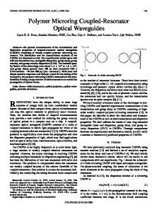
Fig. 3 (a) Schematic diagram of an 8 8 array of microring resonators. Rings with the same waveguide width are drawn with the same point size. (b) Photograph of a portion of the 8 8 array.
2
(1) 4 scattering matrix for node is the column of input wave amplitudes is incident on the node, and the column of scattered wave amplitudes [see Fig. 2(b)]. The elcorrect to first order in the scattering parameter ements of and assuming no polarization conversion are where
is the 4
where is the optical phase delay between the junction posiis the phase tion and the coupling position for the ring, and delay between any two junctions, assuming all junctions are equidistant. is the ring resonator device filter response at the in the absence of the junction), while drop port (i.e., is the straight through response (i.e., in the absence
2
Fig. 4. Scattering response of the 8 8 microring resonator array in Fig. 3. (a) Measured response for path 1 in Fig. 3. (b) Measured response for path 2 in Fig. 3. (c) Calculated response for path 1. (d) Calculated response for path 2.
of the junction.) All scattering elements are with reference to the center of the crossing junction. The remaining elements can be
LITTLE et al.: MICRORING RESONATOR ARRAYS FOR VLSI PHOTONICS
325
found from the symmetry requirement, Analytic expressions are available for and in [2] and [7]. 4 transmission matrix of a node, labeled here as The 4 can be found from the scattering matrix by well known methods [11]. The transmission matrix propagates the amplitudes on the left side of a node to those on the right side, and we therefore write (3) is the column where, of wave amplitudes on the left of a node, and is the column of wave amplitudes on the right of a node [see Fig. 2(b)]. array in Fig. 2(a) is subdivided into The sections as shown by the dashed lines. Each section is described transmission matrix which propagates by a all the waves on the left side of a section to those on the right are easily constructed, with the elements side. The matrices of consisting of: 1) the relevant 4 4 transmission matrices each node in the th section, centered on the appropriate part of 2) diagonal elements equal to unity where the diagonal of there are straight through connections, and 3) zeros everywhere else. Fig. 2(a), for instance, shows the form of the matrices for each section of the 3 3 array. For notational convenience in are 4 4 transmission matrices, the term Fig. 2(a), the terms is a 2 2 unity matrix, and the terms “ ” are either 2 2 zero matrices if they are in the same row as “ ,” or 4 4 zero All matrices are matrices if they are in the same row as rank 12 for the 3 3 array. The overall transmission matrix is a cascade product of the sections (4) The scattering matrix for the entire array is found by transby well known methods [11]. forming matrix I. FABRICATED ARRAY An 8 8 cross grid array of vertically coupled glass microring resonators has been fabricated for test purposes [10]. A top-down schematic of the array is shown in Fig. 3(a), while a photograph of a portion of the array appears in Fig. 3(b). Fabrication details of similar devices can be found in [6]. The rings are nominally all 10 m in radius, have a core refractive index of 1.6532, and a cladding index of 1.4508. The ring waveguide heights are 1.5 m, and the widths vary from 1.0 to 1.7 m in increments of 0.1 m in such a way that along upward directed diagonals the rings are identical [see Fig. 3(a)]. Spacing between parallel bus waveguides is 250 m. Two transmission measurements of this device are considered here, as shown by the labeled paths in Fig. 3(a). In one measurement, the cross-connect response of the upper left corner ring is measured (input 1/output 1). In the second, the signal is cross connected by the same ring, but travels the complete length of two sides of the array (input 2 to output 2). In doing so, this second signal traverses sixteen junctions and interacts with fourteen additional rings. These two measurements are plotted in Fig. 4(a) and (b),
respectively. The signal that traverses the array periphery is attenuated due to the junction scattering loss and by partial extraction by other rings. The power scattering loss per junction is estimated experimentally at 15% (i.e., while the junction scattering into orthogonal waveguides is estimated at Crosstalk scattering has been 1.5% (i.e., reduced to below 30 dB experimentally in other similar devices [6]. Theoretical simulations using the FDTD method predict 1% scattering loss per junction. The observed 15% loss is attributed to the imperfect junction, which showed rounded and flared corners where the two waveguides intersect. Using lower index contrasts can further reduce the loss. Fig. 4(c) and (d) show the predicted responses derived from the analytic theory the exact effective mode indexes using of all rings evaluated by a numerical mode solver, and a ring radius adjusted to match the resonant peak locations of the measured devices (9.96- m radius here). The qualitative response shape and relative power values agree very well with experiments. Particularly, the shape of the noise floors in Fig. 4(a) and (c) and pedestals on the resonant peaks in Fig. 4(b) and (d), are consistent. The noise like ripple on the analytic curves, as in the experimental data, are due to the interference of multiple paths. ACKNOWLEDGMENT The authors gratefully acknowledge Apollo Photonics, Inc., for use of their numerical mode solving software. REFERENCES [1] T. Krauss and P. Laybourn, “Monolithic integration of a semiconductor ring laser and a monitoring photodetector,” SPIE, vol. 1583, pp. 150–152, 1991. [2] B. E. Little, S. T. Chu, H. A. Haus, J. Foresi, and J.-P. Laine, “Microring resonator channel dropping filters,” J. Lightwave Technol., vol. 15, pp. 998–1005, 1997. [3] B. E. Little, J. S. Foresi, G. Steinmeyer, E. R. Thoen, S. T. Chu, H. A. Haus, E. P. Ippen, L. C. Kimerling, and W. Greene, “Ultra-compact Si/SiO2 microring resonator optical channel dropping filters,” IEEE Photon. Technol. Lett., vol. 10, pp. 549–551, 1998. [4] D. Rafizadeh, J. P. Zhang, S. C. Hagness, A. Taflove, K. A. Stair, and S. T. Ho, “Waveguide-coupled AlGaAs/GaAs microcavity ring and disk resonators with high finesse and 21.6-nm free spectral range,” Opt. Lett., vol. 22, pp. 1244–1246, 1997. [5] D. V. Tishinin, P. D. Dapkus, A. E. Bond, I. Kim, C. K. Lin, and J. O’Brien, “Vertical resonant couplers with precise coupling efficiency control fabricated by wafer bonding,” IEEE J. Photon. Technol. Lett., vol. 11, pp. 1003–1005, 1999. [6] S. T. Chu, B. E. Little, W. Pan, T. Kaneko, S. Sato, and Y. Kokubun, “An eight-channel add-drop filter using vertically coupled microring resonators over a cross grid,” IEEE Photon. Technol. Lett., vol. 11, pp. 691–693, 1999. [7] B. E. Little, H. A. Haus, J. S. Foresi, L. C. Kimerling, E. P. Ippen, and D. J. Ripin, “Wavelength switching and routing using absorption and resonance,” IEEE Photon. Technol. Lett., vol. 10, pp. 816–818, 1998. [8] C. K. Madsen and G. Lenz, “Optical all-pass filters for phase response design with applications for dispersion compensation,” IEEE Photon. Technol. Lett., vol. 10, pp. 994–996, 1998. [9] R. A. Soref and B. E. Little, “Proposed N-wavelength M-fiber WDM crossconnect switch using active microring resonators,” IEEE Photon. Technol. Lett., vol. 10, pp. 1121–1123, 1998. [10] S. T. Chu, B. E. Little, W. Pan, and Y. Kokubun, “A cross-grid array of microresonators for very large scale integrated photonic circuits,” in Proc. CLEO ’99, Baltimore, MD, 1999, Paper CPD20. [11] R. E. Collin, Foundations for Microwave Engineering. New York: McGraw-Hill.