Hindawi Journal of Nanotechnology Volume 2018, Article ID 3250932, 23 pages https://doi.org/10.1155/2018/3250932
Review Article Nanobismuth: Fabrication, Optical, and Plasmonic Properties—Emerging Applications Ye Tian 1 2
1
and Johann Toudert2
School of Communication and Electronics Engineering, Hunan City University, Yiyang 413000, China ´ Laser Processing Group (LPG), Instituto de Optica, CSIC, Madrid, Spain
Correspondence should be addressed to Ye Tian;
[email protected] Received 8 December 2017; Accepted 11 April 2018; Published 6 June 2018 Academic Editor: Paresh Chandra Ray Copyright © 2018 Ye Tian and Johann Toudert. This is an open access article distributed under the Creative Commons Attribution License, which permits unrestricted use, distribution, and reproduction in any medium, provided the original work is properly cited. Along the twentieth century, the electronic properties of bismuth have been widely studied, especially in relation with its magnetoresistive and thermoelectric responses. In this context, a particular emphasis has been made on electronic confinement effects in bismuth nanostructures (or nanobismuth). In the recent years, the optical properties of bismuth nanostructures are focusing a growing interest. An increasing number of reports point at the potential of such nanostructures to support plentiful optical resonances over an ultrabroad spectral range: “interband plasmonic” resonances in the ultraviolet, visible, and nearinfrared; dielectric Mie resonances in mid- and far-infrared; and conventional free-carrier plasmonic resonances in the farinfrared and terahertz. With the aim to provide a comprehensive basis for exploiting the full optical potential of bismuth nanostructures, we review the current progress in their controlled fabrication, the trends reported (from theoretical calculations and experimental observations) for their optical and plasmonic response, and their emerging applications, including photocatalysis and switchable metamaterials.
1. Introduction Optical resonances in nanostructures much smaller than the wavelength of light have attracted a broad attention because they allow operating light in small dimensions, for example, allowing efficient harvesting or confinement at the nanoscale [1]. The wavelength of the resonances can be tuned in a static way, by properly engineering the nanostructure composition, shape and size, or a dynamic way through changes in the surrounding medium (its temperature, refractive index, illumination, and so on) [1–7]. Nowadays, a wide range of optically resonant nanostructures rely on the excitation of surface plasmons, that is, the collective oscillations of free charge carriers. Based on the surface plasmon resonances that develop in noble metal nanostructures (Ag and Au) [1, 2], in the visible and nearinfrared, amounts of applications, including surface-enhanced Raman scattering (SERS), photothermal therapy, biosensing, hot carrier generation for photovoltaic conversion, and quantum information processing [8–13], have been demonstrated over the last decades. Since then, surface plasmon resonances have been
achieved with “alternative” plasmonic materials, for example, other metals (Al, Pt, and Pd) [14, 15], transparent conductive oxides [16], metal nitrides [17], doped semiconductors [16], and graphene [18]. Such materials display a plasmonic response in different spectral regions, as dictated by their free charge carrier density N. Note that plasmonic resonances can be excited when the complex dielectric function of the material (ε � ε1 + iε2) shows suitable values, especially having a negative real part (ε1 < 0) is required. Note also that such conditions can be fulfilled without the need of free-carrier excitation, for instance at the high energy side of the strong interband transitions of some p-block elements, allowing the so-called “interband plasmonic” resonances [19]. Bismuth (Bi), as a fantastic p-block semimetal with highly anisotropic Fermi surface, small effective electron mass, low carrier density, and long carrier mean-free path [20–23], is conventionally deemed as a sound candidate to observe and investigate quantum confinement and finitesize effects, enhanced magnetoresistance, and thermoelectricity [21, 22, 24, 25]. In contrast to the very strong interest in the electrical properties of bismuth, its optical response
2
Journal of Nanotechnology z
6
Trigonal θ
4
Hole pocket (T) 2 3
2 Electron pocket (L)
0 –2
1 x
y Energy (eV)
Binary
Bisectrix (a)
–4 –6 –8
EF
–10 T 42 meV
56 meV
36 meV
–12 L
–14 –16
U
X
Γ
L
U
T
H
T-point
L-point (b)
(c)
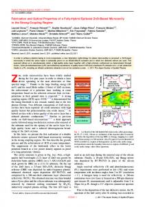
Figure 1: (a) Brillouin zone of bismuth (Bi) in the momentum space: one hole pocket at the T-point and three electron pockets at the T-point. (b) Electronic band structure of Bi near the Fermi level [29, 30]. At room temperature, the direct bandgap at the L-point has an energy of 36 meV, the electron Fermi energy at the L-point is 56 meV, and the hole Fermi energy at the T-point is 42 meV. (c) Full band diagram of Bi calculated by the third-neighbor tight-bonding model accounting for the spin-orbit coupling. Reprinted from [31] © 2015 Fuseya et al., originally published in Journal of the Physical Society of Japan, vol. 84, p. 012001, 2015, doi: 10.7566/JPSJ.84.012001, under CC by 4.0 license.
has been less studied over the past. Few works reported the optical properties of bulk Bi and Bi thin films and even less for Bi nanostructures (or “nanobismuth”). Very recently, Bi has become increasingly attractive mostly due to the potential of its nanostructures to support optical resonances in the ultraviolet (UV), visible (Vis), and near-infrared (nearIR) regions. It has been proposed that such resonances have an “interband plasmonic” origin. Besides, a “traditional” free-carrier-based plasmonic response is expected in the farIR to terahertz (THz), and dielectric Mie resonances have been recently predicted in the mid-IR to far-IR region. Moreover, along with the theoretical and experimental studies on the optical response of Bi nanostructures, their potential for emerging applications, such as switchable metamaterials or photocatalysis [7, 26], are also being explored. In this review paper, we summarize the advances in the field of the optical and plasmonic properties of Bi nanostructures over the last years. After a synthetic presentation of the optoelectronic properties of bulk Bi, we review the progress in the fabrication of Bi nanostructures, in the theoretical calculations and experimental observations of their optical and plasmonic responses, and the works
about the related emerging applications. Such a review will help to assess the potential of nanobismuth as a new material for plasmonics and nanophotonics with ultrabroad spectral response from the UV to THz region.
2. Optoelectronic Properties of Bulk Bismuth 2.1. Electronic Band Structure. Bi is a semimetal with unique physical properties, including long charge carrier mean-free path (∼1 micron at room temperature) [27], huge magnetoresistance [24], or quantum confinement effects in nanostructures with dimensions of tens of nanometers [28]. Such peculiar features originate from the peculiar electronic band structure of the rhombohedral Bi, which presents a highly anisotropic Brillouin zone [29]. Such an anisotropy is exemplified in Figure 1(a) [29], which illustrates the existence of different carrier pockets depending on the spatial direction. Near the T-point of the Brillouin zone, Bi has one hole pocket (hole Fermi surface (FS), aligned ellipsoidically with the trigonal axis z). Near the three equivalent L-points, there are three identical electron pockets (electron FS ellipsoids arrayed symmetrically around the hole FS with a small tilted angle
Journal of Nanotechnology (∼6.5°) out of the plane defined by the bisectrix and binary axes). These three equivalent L-points have both conduction and valence bands, separated by a small bandgap of 36 meV at room temperature (Figure 1(b)) [30, 31]. The Fermi level is located in the conduction band at the L-point and in the valence band at the T-point: this produces semimetallic characteristics where electrons and holes coexist, as shown in Figure 1(b). As a consequence of this semimetal character, Bi presents a very low free-carrier density (NBi, in the range from 1018 to 1019 cm−3). Beyond this semimetallic character that arises from the electronic band structure near the Fermi level, it is worth mentioning that Bi has a rich variety of lower-lying energy bands as demonstrated in the band diagram of bismuth (Figure 1(c)), which have been predicted early theoretically [32, 33] and probed by photoelectron or optical spectroscopy. As we will see below, electronic transitions from lowerlying energy bands can be probed optically in the UV, Vis, and IR regions, whereas the free charge carriers involved in the semimetallic conduction of Bi can be probed only with far-IR and THz light. Indeed, optical absorption by the free charge carriers of Bi becomes relevant in the far-IR-THz regions, owing to their low plasma energy Ep,Bi � h√(NBie2/4π2mε0) ≈ 0.05 eV that results from the very small value of NBi. 2.2. The Optical Dielectric Function of Bulk Bismuth. Although Bi is an interesting element with a rich electronic band structure that impacts its optical response, as discussed in Section 2.1, the optical properties of Bi have been less explored than the electronic ones [24, 28, 29]. Especially, the optical dielectric function ε � ε1 + iε2 of bulk Bi was reported early by several authors, but in limited spectral regions, and shows a broad dispersion (related mostly with a limited sample quality) as seen in Figure 2. It is only recently that works providing a refined optical characterization of Bi crystals and films were reported [33–35]. Especially, a systematic spectroscopic ellipsometry characterization from the far-IR to the UV was performed on high quality Bi films to provide an artefact-free and Kramers–Kronig consistent dielectric function of the Bi material [19]. In this work, only the dielectric function standing for the in-plane response of the films (i.e., perpendicular to the trigonal axis) was determined. Yet, although the dielectric function of Bi crystals along the trigonal axis has been probed early in the near- to mid-IR showing no marked optical anisotropy in this region, it remains to be measured accurately in a broader spectral region (discussion and related references in [35]). From the dielectric function shown in Figure 2, it is seen that ε1 < 0 in the UV, visible, and near-IR regions, thus allowing a plasmonic response in this region. It has been shown in [35] that such negative ε1 originates from the strong interband transitions peaking at 0.8 eV, whereas the negative ε1 in the far-IR and THz originates from the freecarrier contribution. In sum, Bi nanostructures have the potential to display plasmonic effects in two spectral regions: (i) in the far-IR and THz due to the collective excitation of free carriers and (ii) in the UV-Vis-near-IR regions where, unlike the conventional plasmonic resonances of noble
3 metals driven by the collective excitation of free electrons, the resonances in Bi nanostructures would be totally induced by interband transitions and called “interband plasmonic” resonances [19]. Furthermore, in between these two plasmonic regions, ε1 takes very high positive values, thus making Bi an interesting candidate for supporting dielectric Mie resonances in nanostructures at mid- and far-infrared wavelengths.
3. The Growth of Nanobismuth Amounts of Bi nanostructures have been successfully prepared: 0D nanostructures (including nanoparticles, nanospheres, and nanocubes), 1D nanostructures (including nanowires, nanorods, and nanotubes), and 2D nanostructures (including nanoplates, nanosheets, and thin or ultrathin films), with continuously improved crystalline quality [36–58]. The size of these structures covers the range from a few atoms to few microns, which has allowed a wide suitability for studies in various fields including quantum transport, thermoelectricity, topological insulators, giant magnetoresistance, and superconductivity [24, 59–62]. Such size control is also especially relevant for the fields of plasmonics and nanophotonics, where the working wavelength of the system is closely related to the dimension of the nanostructures. The wide size range of the existing Bi nanostructures would thus provide abundant building blocks to construct optical systems suitable for different wavelength ranges from the UV region to the far-IR and THz regions [34, 35, 63–65]. As the precondition of the studies to the properties of nanobismuth, its fabrication methods were explored intensively over the past few years. They can be divided into two groups: one is template based, where selected matrices are used to prepare the Bi nanostructures [60, 66–70], and the other is template free. In the latter case, many techniques are used. Stress effects are quite useful for fabricating the Bi nanowires [27, 71]. Physical vapor deposition (PVD, mainly RF sputtering and thermal evaporation) has demonstrated its potential for the mass production of Bi nanowires and nanorods, as well as tilted Bi nanocolumns [39, 40, 42]. Solution-phase synthesis allows fabrication of Bi nanostructures with a wide control in their shape, either for 0D, 1D, and 2D nanostructures [24, 45–48, 54, 58, 72, 73]. Laserinduced approaches have been successfully used to produce Bi thin films, nanorods, and nanoparticles [34, 35, 43, 51, 63]. Molecular beam epitaxy (MBE), electron-beam lithography (EBL), electron-beam irradiation, electromigration (EM), and plasma force have also been used [53, 57, 62, 74]. In the following, these methods will be discussed one after another. 3.1. Template-Based Method. Template-based methods used for growing Bi nanostructures rely mostly on the use of anodized aluminium oxide (AAO) templates, which serve as the host material with a uniform porous structure, as shown in Figure 3(a) [75]. By tuning the anodization parameters, the pore diameter and packing density of AAO can be well controlled [67, 75]. In such AAO templates, arrays of Bi nanowires were grown by filling the pores by pressurized injection of liquid Bi (the liquid-phase method), by
4
Journal of Nanotechnology
5
2
(μm) 1
0.5
20
10
2
1
Near-IR
10
Short-wave IR
(μm) 20
5
0.5
2
100 100
9 8 7 6 5
50
4
ε2
ε1
3 2
0
–100
2 4 6 8
2
4 6 8
0.1 1 Photon energy (eV)
This work Hunderi 1975 Toudert 2012 Hodgson 1954
2
4
4 6 8
Lenham 1965 (basal) Lenham 1965 (o.a.) Khalilzadeh 2015 (Th)
(a)
2
4 6 8
0.1 1 Photon energy (eV)
UV
3
Far-IR
4
Mid-wave IR
–50
Long-wave IR
9 8 7 6 5
Visible
10
2
4
Khalilzadeh 2015 (e) Tediosi 2007 Harris 1963 (b)
Figure 2: Broadband dielectric function (ε � ε1 + iε2, black) of bulk Bi together with literature data, showing their broad dispersion. The origin of these data and the reasons behind their dispersion (mostly in relation with the sample quality) are discussed in [34, 35]. Reprinted with permission from American Chemical Society.
electrochemical deposition, or by vapor-phase deposition, as shown in Figures 3(b)–3(e) [60, 67, 68]. Using pressurized injection, most Bi nanowires could be single crystalline along the [202] direction in the hexagonal lattice with a broad diameter tunability range (12–109 nm), but they experience high stress [75]. If using the electrochemical or vapor-phase deposition methods, the nanowire diameter could be further reduced to 7 nm [20]. Moreover, upon rational choice of the parameters for electrochemical deposition, Bi nanotubes can also be prepared (Figure 3(f)) [76]. The main drawbacks of the AAO template methods are the small aspect ratio and surface irregularities of the fabricated nanowires or nanotubes. Moreover, due to the difficulty in removing the AAO and subsequently extracting individual nanowires or nanotubes [76–78], the characterization of samples based on the AAO templates provided mostly ensemble measurements over the whole array. Also, in these cases, the influence of the AAO on the macroscopic properties of the sample is hard to be subtracted. Unlike the AAO template method, the Ulitovsky method can be used to obtain individual nanowires [68, 70]. It
involves a two-step process. Firstly, Bi is inserted in a borosilicate glass capsule where it is heated by a high-frequency induction coil. Secondly, the softened capsule as well as the molten Bi within (note that the melting temperature of bulk Bi is only 271°C) is drawn out by spooling. This method can produce ultralong single-crystalline Bi nanowires along [111] direction in a conventional hexagonal lattice system with diameter down to 55 nm, as shown in Figure 4(a) [70]. Moreover, the surface oxidization to the nanowires can be avoided since in this process the molten Bi is not air-exposed [41]. The optical transparency of the glass is interesting for nanophotonics or plasmonics studies. Quartz can also serve as a template, upon digging holes using optical fibers, following a method comparable with that applied in the manufacture of hollow-core photonic crystal fibers [79]. Hence, similarly with the pressurized injection process that is used with AAO templates [75], the molten Bi can be injected into the holes of the quartz templates where the Bi nanowires form (Figure 4(b)) [80]. Although the quartz template method has several benefits, such as achievable nanowire lengths comparable with the
Journal of Nanotechnology
5 Cell size
Pore diameter
(b)
(a)
Alumina film
(c)
V V
Barrier layer Aluminum substrate
Top
M2+ M2+
2+ M2+ M 2+ M + 2e– → M M2+ M2+ M2+ M2+ M2+
Bottom 500 nm (d) Clip
Porous alumina host plate
Vacuum chamber
(e)
(f)
Bi drop Top plate Bi vapor Liquid Bi
Spacer plate Heater windings Crucible 100 nm
Pump
Figure 3: (a) Scanning electron microscope (SEM) image of an anodized aluminium oxide (AAO) template. (b) Growth mechanism in the liquid-phase method with an AAO template. (c) Schematic illustration of the electrochemical deposition in the AAO pores to fabricate nanowires. (d) Schematic diagram of the vacuum chamber, including a crucible for growing the nanowires by vapor-phase deposition. (e) SEM image of Bi nanowires in an AAO template. (f) SEM image of Bi nanotubes prepared by electrochemical deposition in an AAO template. Reprinted with permission from [75] Cambridge University Press, [76] American Institute of Physics, and [77] American Physical Society.
(b)
(a)
Glass tube Bismuth melt Induction furnace coil Spool
Figure 4: (a) Cross-sectional SEM image of a Bi nanowire grown by (a) the Ulitovsky method (the inset diagram outlines the growth mechanism) [70] and (b) pressurized injection in a quartz template [80]. Rreprinted with permission from [69] American Physical Society and [79] © 2012 Masayuki et al., originally published in Nanoscale Research Letters, vol. 7, p. 505, 2012, doi: 10.1186/1556-276X-7-505, under CC by 2.0 license.
Ulitovsky method [68, 70], negligible contamination, and smaller optical loss of quartz in comparison with borosilicate glasses, the hole and accordingly the diameter of the nanowires (∼100 nm) seems yet too large to achieve optimal performance in some applications such as those requiring optical resonances in the UV region [7]. 3.2. Stress-Induced Method. In several composite films with immiscible components such as Bi-CrN [71], Bi-Al [81],
and Bi-Co [82], the compressive stresses could force the Bi to squeeze out and form nanowires. Utilizing the difference between the thermal expansion coefficients of the Bi thin film and a substrate or cap layer [27, 83], the compressive stresses can be also introduced by heating close to the melting temperature of Bi, and accordingly the Bi nanowires grow to release the induced thermal stress (Figures 5 (a) and 5(b)). Such stress-induced method is named as OFF-ON (on film formation of nanowires) and has been extended to other systems [27, 84]. In this method, the
6
Journal of Nanotechnology
(a)
Sputtering Bi thin film (TF)
(b) Bi SiO2 Si
Annealing Compressive stress induced in Bi TF
(c)
Cooling Completion of Bi NW growth onto Bi TF
Figure 5: (a) Schematic representation of the growth mechanism by the OFF-ON method. (b) SEM image of the grown Bi nanowires. (c) Transmission electron microscope (TEM) image of a Bi nanowire and its electron diffraction patterns and crystal structure [27]. Reprinted with permission from American Chemical Society.
nanowire length and diameter can be controlled, respectively, via the heating time and the grain size of the Bi thin film deposited, for instance, on a thermal-oxidized silicon wafer (diameters between 21 nm and 10 μm and lengths up to several millimeters) [27]. The nanowires present a rather random orientation on the substrate (Figure 5(b)), but their growth occurs with a major crystal orientation in the [100] direction (Figure 5(c)) [27]. As a template-free method, the obtained Bi nanowires are free of the contaminations from chemical solutions or templates. However, because such nanowires do not present any initial passivation layer over the surface, further oxidation could generate during the fabrication or characterization (e.g., Raman spectra measurement) [85, 86]. 3.3. PVD Growth of Bi Nanowires. Recently, it was found that vapor-deposition of Bi in specific conditions enables the spontaneous growth of nanowires [38, 41, 87, 88]. The attraction toward the PVD growth of Bi nanowires is that it can more readily produce structures that have a high degree of perfection in terms of crystallinity and regularity of the surface [38, 41, 87, 88]. Moreover, this method allows achieving a scalable nanowire growth and particularly dense wire populations [41, 87]. A higher conversion yield (>70%) from the deposited material to nanowires is also possible compared with the few-percent conversion of the stressinduced method [39]. Table 1 gathers selected cases for the
PVD-growth of Bi nanowires reported in recent years: the processing temperature is relatively low (RT-200°C), the wire diameter ranges from 50 nm to 1 μm, and the length could reach tens of microns. Although the growth mechanisms of the Bi nanowires are under intense debate [86], generally, they can be catalogued into two main kinds: tip growth and root growth [39, 86]. In most reports about the PVD growth of Bi nanowires, the tip-growth mode (as shown in Figure 6(a)) seems to dominate. The growth starts from specific nuclei that form on the (initially) deposited bismuth film (step i to step ii), which might be screw dislocations, whiskers, hillocks, and grains [38, 86, 88]. These nuclei are related with lattice planes for preferential growth, which could be (110), (111), or (012) facet [41, 86]. Afterwards, the incoming Bi atoms would continuously migrate to preferential facets (step ii to step iii), resulting in the nanowire formation along the preferential direction with the growth front at its tip as shown in Figure 6(b). The wires with [110] or [012] orientation was found in the tip-growth cases [38, 40, 42]. The deposition rate has to be relatively low to provide a long adatom diffusion time [42], and accordingly, the growth of the nanowires is slow (typically it takes ten minutes to grow a ∼10 μm nanowire) [38, 86, 88]. Moreover, high-rate diffusion of Bi adatoms is necessary for their long-distance motion to the tip. Therefore, sufficient kinetic energy and substrate heating are usually required [88]. Of course, if the deposition rate is low enough, the 1D growth is still
Journal of Nanotechnology
7 Table 1: The direct growth of Bi nanowires by PVD methods.
Temperature (°C)
Deposition rate (nm/s)
Length (μm)
Diameter (nm)
Growth time (min)
Tip growth RF sputtering
200
0.67
∼10
140
10
RF sputtering
200
0.7
10s
100∼300
10
110∼140
0.04∼0.12
16 ± 1
500
70∼210
Glass, Si (100), Si (111), and GaAs (100) [38]
120 RT∼200
0.03∼0.09 0.044∼0.341
3∼16 3∼40
80∼120 80∼400
18.5∼55 40
Si (111) [40] Si and glass [41]
120∼160 0∼75
4 0.1∼0.2
10∼50 0.5∼30
171∼1800 60∼200
4 4.2∼8.3
Glass [87] Porous vanadium film [39]
Growth technique
RF sputtering and thermal evaporation RF sputtering RF sputtering Root growth RF sputtering RF sputtering
Bi
Substrate
Si (111) [88] Transition metal films (Fe, Ni, and Co) and W, Pt, and Au on oxidized Si, Si (111), oxidized Si (100), and fused quartz [86]
Bi
(i)
(ii)
Bi
Bi
(iii) Nanowire Bi adatom
Substrate (Initial) film Nuclei (a)
(b)
Figure 6: (a) Schematic representation of the tip-growth mode. (b) SEM image of Bi nanowires following the tip-growth mode. Reprinted from © Steven Antony Stanley, “The growth, structure and electrical properties of PVD deposited thin films and nanostructures of bismuth and antimony [D]” (2009), under CC by 2.5 license.
possible at room temperature and even by deposition with thermal evaporation, despite the formed nanowires being rather short (i.e., the growth becomes very slow) [42]. Additionally, it is noteworthy that, in the tip-growth mode, as the deposition time is long enough, the nanowire growth stops when a certain nanowire length is reached because the diffusing atoms are too far away from the tip to reach it [86]. For the root-growth mode, the extrusion of Bi on porous vanadium is a representative example [39]. In this case, first, Bi is deposited on a columnar vanadium thin film into which it infiltrates (Figures 7(a) and 7(b)). Due to the low wetting of vanadium with Bi, Bi exodiffuses from the pores and agglomerates at the surface to form a nucleation center (Figure 7(c)). Later in the deposition, incoming Bi atoms diffuse toward the nucleation centers where nanowires grow along the [012] direction with the growth front at their root (Figure 7(d)) [39]. Figure 7(e) shows the cross-sectional
transmission electron microscopy (TEM) image of a Bi nanowire on the vanadium film as well as the energy dispersive X-ray spectra (EDX) mapping near the nanowirevanadium film interface. Probably because a timeconsuming adatom surface diffusion to the tip is not needed in the root-growth mode, the wire-growth speed (typically, it takes just few minutes to grow to ∼10 μm length) seems faster than the tip growth [39]. Such a mechanism may also take effect in the quick nanowire growth along the [110] direction during the high-rate deposition of Bi on glass [87], where the initially deposited Bi atoms form nanoparticles which might play a role very similar to that of the agglomerated domains on columnar vanadium thin film [39]. However, without the excess surface energy provided by a columnar morphology to enable the highly directional and ballistic motion of the incoming Bi, a high deposition rate is needed to supply plenitudinous Bi timely for (fast) root growth [87].
8
Journal of Nanotechnology Vanadium film
(i) Bi deposition
Substrate (b) (ii) Bi extrusion
(a) Bismuth nanowire
Recurring Bi deposition and extrusion from root
Nucleation center (d)
(c)
V (K, 4.952 keV)
Bi (M, 2.419 keV)
V + Bi (e)
Figure 7: (a–d) Simplified representation of the growth of a Bi nanowire on a vanadium film following the root-growth mode. (e) TEM image of a Bi nanowire on the substrate. The energy dispersive X-ray (EDX) mapping of the distribution of the different species is also shown [39]. Reprinted with permission from the American Chemical Society.
3.4. Chemical Synthesis of Nanobismuth. Several chemical synthesis strategies, including the hydrothermal process, solution-phase process, thermolysis method, bottom-up assembly, polymer-assisted polyol process, solvothermal growth, aqueous chemical route, and electrochemical deposition, are widely applied for preparing a wide variety of Bi nanostructures such as nanobelts, nanosheets, nanospheres, nanowires, and nanotubes [26, 44–46, 48, 50, 54–56, 58, 72, 73, 89–91]. Although the starting materials and the synthesis conditions, as well as the growth mechanisms, in these reports show markedly different features, the growth processes can be divided into three steps as shown in Figure 8(a): (1) the reduction of Bi precursors into
Bi. In this step, several materials, such as NaBiO3, Bi [N (SiMe3)2]3, Bi(NO3)3, biacetate, bicitrate, and BiCl3, can serve as the Bi source to be reduced; (2) the agglomeration of Bi into nuclei; and (3) Bi nanostructure growth from these nuclei in a liquid phase including a dispersant or surfactant (such as polyethylene glycol, poly(1-vinylpyrrolidone)-graft-(1-hexa, decene) cetyltrimethylammonium bromide, sodium oleate, polyvinylpyrrolidone, and oleylamine). Such products, which are usually but not always needed, provide a spatially constrained reaction environment. Note that an intrinsic anisotropy, such as different surface energies at different lattice facets, or an externally produced anisotropy, allows synthesizing final products with a nonisotropic shape. Therefore,
Journal of Nanotechnology
9
(a)
Bi5+/Bi3+
Bi Reduction
Nucleation Growth
(b)
(c)
500 nm
(d)
(e)
100 nm
200 nm
Figure 8: (a) Schematic representation of the Bi nanostructure growth by solution synthesis. TEM image of (b) Bi nanowires [44], (c) Bi nanobelts [73], (d) Bi nanoplates [47], and (e) Bi nanoparticles [52] prepared via solution synthesis, and the scale bar in (c) is 100 nm. Reprinted with permission from the American Institute of Physics and American Chemical Society.
upon rational tuning of the synthetic parameters and reaction conditions, the size and shape of the Bi nanostructures can be well controlled (Figures 8(b)–8(e)), and different lattice orientations were observed. However, due to the potential contamination from the solvent, dispersant, or surfactant, the crystalline quality of the products is poorer than that obtained following the stress-induced or PVD growth methods.
3.5. Laser-Assisted Processing. Bismuth nanostructures can also be prepared by laser-assisted methods. Basically, using these methods, a laser beam is used to vaporize or ablate Bi from a target, and then the products are collected on a substrate or directly dispersed in a liquid as shown in Figures 9(a)–9(c). The process can be carried out in a vacuum chamber, as done for the pulsed laser deposition (PLD) of Bi thin films or Bi nanoparticles embedded in an Al2O3 matrix [35, 63]. It can also be carried out using Ar gas as the matter-transport media, as done for the preparation of Bi nanoparticles by pulsed laser ablation (PLA) [37]. Using the Bi target containing 1% of Au catalyst, and using an Ar/H2 mixed gas as matter-transport flow, a Bi nanorod growth was found to occur along the [012] direction [43]. Bi nanoparticle growth was also reported by ablation in liquids such as lubricant oils, where the obtained colloidal solution could be very suitable for tribological applications [51]. The crystalline quality of the products prepared by laser-assisted methods is moderate (Figures 9(d) and 9(e)), but the shortcoming is their relative broad size-distribution and/or poor shape-control as shown in Figures 9(f) and 9(g) [51].
3.6. Other Methods. Other methods to prepare Bi nanostructures include EBL [74], EM [61], MBE [62, 92], thermal decomposition [50], electron-beam irradiation [53], hydrothermal etching [46], and plasma force [57]. The EBL method is suitable for well defining the position, the shape, and the dimension of the nanostructures but expensive and limited to small area samples. The EM method can yield [110]-oriented Bi nanowires, with a diameter that can be reduced by a precisely controlled current though the wire. Bi atoms deposited on graphite surface by MBE showed 1D growth driven by anisotropic corner crossing. Bi nanoparticles were also obtained by thermal decomposition of Bi granules or prepared in situ under electron-beam irradiation to sodium bismuthate. Bi nanospheres on a Si surface were prepared by using low energy plasma focusing, or hydrofluoric acid-free hydrothermal etching.
4. Optical and Plasmonic Properties of Nanobismuth 4.1. UV-Vis-Near-IR Spectral Region 4.1.1. Theory: Interband Plasmonic Resonances in Bi Nanostructures. As explained in Section 2.2 in the UV-Visnear-IR spectral region, the real part of the dielectric function of bulk Bi takes negative values (ε1 < 0). Assuming that the dielectric function of Bi nanostructures is comparable to that of bulk Bi, this makes possible a plasmonic behavior for such nanostructures in the UV-Vis-near-IR. For a spherical
10
Journal of Nanotechnology Substrate
Laser beam Lens
Heater
Laser Target carousel
To pump
Glass cell
Plasma pulm
Solution
Oxygen inlet Target
(a)
(b)
Water in Vaccum pump
Motor-driven reflector
Rotating target
Ar, H2 in Quartz tube Water out
Furnace
Cold finger Nd:YAG laser (c)
(d)
(e)
Figure 9: Continued.
Journal of Nanotechnology
11
20
25 20 Counts
Counts
15
10
15 10
5
0
5
8
10
12
14 16 Diameter (nm)
18
20
22
(f)
0
100
150
200 Length (nm)
250
300
(g)
Figure 9: Schematic representation of laser-assisted fabrication of Bi nanostructures (a) in vacuum, (b) with matter-transport gas, and (c) in a liquid. (d) TEM image of a Bi nanorod produced by laser ablation and (e) its corresponding lattice fringes. (f) Diameter and (g) length distribution of the Bi nanorods [43]. Reprinted with permission from Reppert, Jason, “Laser-assisted synthesis and optical properties of bismuth nanorods” (2007), All Theses, 188.
nanostructure much smaller than the wavelength of the incident light and with e2 weakly dependent on E, quasi-static plasmonic resonance with a dipolar character occurs at the photon energy where ε1(E) � −2εm, with εm being the realvalued dielectric function of the surrounding medium. This relation, also known as the Fr¨ohlich condition, is fulfilled in the near UV for a Bi nanosphere in the usual embedding media such as SiO2 or Al2O3 and can be approached in the visible region upon increasing εm [63]. For nonspherical Bi nanostructures, several quasi-static resonances are expected at different photon energies depending on the polarization of the incident light and on the nanostructure shape. For instance, in the case of spheroidal nanostructures, the Fr¨ohlich condition becomes ε1(E) � (1 – 1/Lu)εm, where Lu is the shape-dependent depolarization factor of the nanostructure along the direction u (along the spheroidal revolution axis or perpendicular to it). According to this relation, Bi nanospheroids can display two dipolar resonances: one for light polarized along the revolution axis (longitudinal resonance), and one for light polarized perpendicular to it (transverse resonance). Upon decreasing (increasing) the height-to-diameter ratio (or aspect ratio) of the spheroid, the transverse resonance shifts toward smaller (higher) photon energies and the longitudinal resonance toward higher (smaller) photon energies. This makes possible to bring one of the resonances deeper in the UV region than that of a Bi nanosphere and to drive the other across the visible toward the near-IR. This behaviour is thus comparable to that of localized plasmon resonances in noble metal (Ag and Au) nanostructures, however with a different origin. Instead of involving a collective oscillation of free carriers, they stand on the excitation of interband transitions that make the ε1 of Bi turn negative in the UV-Vis-near-IR regions. Therefore, the term of “interband plasmonic” resonances has been proposed [35]. With the aim of addressing more quantitatively the features of such resonances than with the simplified picture
of the quasi-static limit, several works have reported the use of analytical or numerical methods to compute the optical response of Bi nanostructures with sizes smaller or comparable with the wavelength of the incident light. Finite element method (FEM) [7], Mie [35, 54], and finite difference time domain (FDTD) [93] calculations have been used to simulate the optical cross sections of Bi nanospheres and their near-field enhancement for diameters up to a few hundreds of nm. The modified long wavelength approximation (MLWA) has been used to simulate the transverse optical cross sections of flattened Bi nanospheroids with diameter up to a few hundreds of nm [63]. FDTD calculations have been done to predict the transverse and longitudinal optical cross sections of Bi nanorods with lengths up to a few hundreds of nm and their near-field enhancement [64]. Maxwell’s equations solving with the volume integral equation FFT method have been used to compute the optical extinction cross section of Bi nanospheres and nanoprisms and their near-field enhancement [94]. From these works, several predictions can be underlined: (i) Upon increasing the diameter of a Bi nanosphere from a few nm to a few hundreds of nm, its extinction spectrum passes from being dominated by a single dipolar resonance that shifts from the UV to the visible region, to becoming a superposition of multiple order resonances spanning over the far UV-visiblenear-IR region and showing no clear maximum in the visible [7, 93], as exemplified in Figure 10(a). (ii) The dipolar resonance dominates the extinction spectrum of a Bi nanosphere while its diameter is lower than 100 nm. In these conditions, the resonance peaks in the UV or violet region (for a usual εm), where the extinction efficiency reaches values near 5 with a marked contribution of absorption
12
Journal of Nanotechnology Photon energy (eV) 4
3
Extinction and absorption efficiencies
5
0 5
2
Plane waves
1
Ext
Bi particle
D = 50 nm
Abs 100 nm
0 5
T 6.15 6 4
200 nm
2 0 5
0.15
400 nm
0 400
600 800 1000 1200 Wavelength (nm)
1400
(a)
(b)
1400 Pol Pol
1000
itudi nal Long
800
erse nsv Tra
Resonance wavelength (nm)
1200
600
400
4 6
0.1
2
4 6
2
1 Aspect ratio
4 6
10
2
(c)
Figure 10: (a) Simulated extinction and absorption efficiency spectra of spherical Bi nanospheres of different diameter D, in water. Simulations have been done using the Mie theory and the dielectric function of Bi given in Figure 1. (b) Simulated near-field intensity (reprinted with permission from [105] © 2015, American Chemical Society). (c) Simulated resonant wavelengths of Bi nanospheroids in water, as a function of their aspect ratio. Simulations have been done using the Gans theory and the dielectric function of Bi given in Figure 1. For an aspect ratio 1), the transverse (longitudinal) resonance occurs in the UV-to-near-IR regions.
(Figure 10(a)). Such value is comparable with those found in the visible region for several metals and higher than those of Ag and Au nanostructures in the UV region [7, 93]. (iii) For a Bi nanosphere of any diameter, the dipolar and higher order resonances have a small quality
factor (i.e., a broad spectral width) and induce a very small near-field enhancement (Figure 10(b)), due to the significant ε2 values of Bi in the whole UV-Visnear-IR region [63, 93]. (iv) The dipolar resonances of Bi nanorods or nanocylinders can be tuned across the UV to near-IR
Journal of Nanotechnology region, with the corresponding extinction cross section remaining near 5, by controlling the nanostructure aspect ratio [63, 64] (Figure 10(c)). From such results, it is evident that Bi nanostructures are interesting candidates for applications that require a strong absorption of light tunable in a broad spectral range from the UV to the near-IR region, such tuning being expected upon proper design. However, they are not suitable if high nearfield enhancements or resonances with large quality factor are needed. 4.1.2. Experimental Observations. There is an increasing number of works reporting measurements of the UV-Visnear-IR optical spectra of Bi nanostructures. The analysis of such reports provides valuable information for assessing the validity of the theoretical trends described above. The earliest well-documented experimental work about the optical response of Bi nanostructures in the UV-Vis-nearIR was focused on solution processed Bi nanospheres diluted in water, with a diameter of D < 10 nm [95]. These nanospheres showed an absorption band in the mid-UV that was attributed to a plasmon resonance. More recent works reported the absorbance spectra of Bi nanospheres with a broader range of diameters: D < 10 nm, polydisperse Bi nanospheres with a low volume fraction in a glass matrix fabricated by melt quenching [96]; D � 10 nm, nearly monodisperse solution-processed Bi nanospheres diluted in hexane [97]; 10 nm < D < 80 nm, solution-processed polydisperse Bi nanospheres diluted in ethanol [54]; D � 100 nm, vapor-deposited Bi nanospheres located with a low surface density at the mouths of an hexagonal-anodized TiO2 honeycomb array [98]; and 50 nm < D < 1 μm, nearly monodisperse surface-oxidized solution-processed Bi nanospheres as a dried powder [99]. A trend seems to emerge from these works, as seen in Figure 11(a). The absorbance spectrum of the nanostructures with D ≤ 10 nm is dominated by a band peaking in the UV region. That of the polydisperse nanostructures with 10 nm < D < 100 nm consists of a broad band spanning in the visible region from blue to red photon energies. That of the biggest surface-oxidized Bi nanospheres spans over the whole visible region with no clear maximum. These trends are in qualitative agreement with the theoretical ones described above—point (i)—that predicted a shift of the dipolar interband plasmonic resonance from the UV to the visible region upon increasing D, followed by the onset of higher order resonances that yield a featureless extinction spectrum across the visible region. Other works reported the UV-Vis-near-IR absorbance spectra of Bi nanostructures with nonspherical shapes, showing trends in agreement with theoretical predictions—point (iv) above. The absorbance spectra of coalesced Bi nanostructures in an Al2O3 medium was shown to include absorption bands characteristic of longitudinal and transverse resonances, the former being dominant and shifting from the near UV to the near-infrared as the nanostructure shape becomes more anisotropic, as seen in Figure 11(b) [63]. Pulsed laser-vaporized Bi nanorods in chloroform, with an aspect ratio of 20,
13 displayed an absorption band in the near UV, attributed to a transverse plasmon resonance [100]. The spectral region of the measurement did not reach the photon energies where the longitudinal mode is expected for such aspect ratio. Besides, the absorbance spectra of hybrid structures consisting of Bi nanostructures grown on dielectric nano- or microstructures (platelets, wires, and particles) have been reported in many works. In such structures, the Bi-related absorption peaks in the UV region for small Bi coverages and gradually extends to the whole UV region as the Bi coverage increases, as seen in Figure 11(c) [101–106]. This trend could be ascribed to the increasing size and degree of percolation of the Bi nanostructures as their coverage increases.
4.1.3. Quantum Confinement. Many of the trends observed experimentally for the UV-Vis-near-IR optical response of Bi nanostructures can be qualitatively accounted for by classical modeling. With such modeling, the dielectric function of the nanostructures is assumed to be the same as that of bulk Bi. However, several works have also proposed that quantum confinement effects in Bi nanostructures can modify their dielectric function compared with the bulk. Such modification could affect their optical properties in the UV-Vis-near-IR region. When the size of a nanostructure becomes small enough (typically, smaller than the free charge carrier mean-free path in conductors, or exciton Bohr radius in excitonic semiconductors), its electronic structure (and thus its dielectric function) can depart from that of the corresponding bulk material and depend on the nanostructure size. In Bi nanostructures, it was proposed that such confinement effects can trigger a semimetal to semiconductor transition, which was reported first in thin films at a critical thickness near 30 nm [107]. The confined semiconducting Bi presents a bandgap that widens upon decreasing the nanostructure size. It was proposed that such bandgap widening can be strong enough so that the bandgap energy Eg reaches the UV-Vis-near-IR region (Eg > 0.8 eV) [108]. Such mechanism was used to interpret the blueshift in the optical absorption onset across the near-IR and visible regions for nanoparticles with truncated spheroidal shapes grown by sputtering deposition on transparent substrates, upon varying their size from a few tens of nm to a few nm [108]. In this work, the nanoparticle size was varied by tuning the amount of deposited Bi through the deposition time. By such method, it is worth noting that the shape and coverage of the nanoparticles vary together with their size. The same mechanism was also used to explain the near-IR absorption onset observed for D � 3 nm Bi nanospheres [109], and not for a bismuth powder. The existence of a bandgap widening due to confinement in Bi nanostructures was also discussed from the observation of their EELS spectra in the spectral region of their volume plasmons [52, 110, 111]. 4.1.4. Partial Conclusion. Although a significant number of works have already reported the UV-Vis-near-IR optical
14
Journal of Nanotechnology 1.0
100–200 nm 0.9
200 nm–1 μm
50 nm
0.6 50 nm 0.4 10 nm 0.2
Optical transmittance
Normalized absorbance
0.8
0.8
0.7
D < 10 nm 0.6
0.0 400
600
800 1000 1200 Wavelength (nm)
1400
400
800 1200 Wavelength (nm)
(a)
1600
(b)
1.0 0.9
Bi
Absorbance (a.u.)
0.8
B0.5Z
0.7 0.6 0.5 0.4 ZnWO4
0.3
B0.5Z
ZnWO4
0.2 0.1
Bi
200
300
400 500 600 Wavelength (nm)
700
800
(c)
Figure 11: (a) Compilation of experimental absorbance spectra of Bi nanospheres (in liquids) with different diameters taken from the literature: