Optical absorption and quantum efficiency in the resonant-cavity detector with anomalous dispersion layer. S. V. Gryshchenkoa, A. A. Dyomina, V. V. Lysakb, I. A. ...
NUSOD 2008
Optical absorption and quantum efficiency in the resonant-cavity detector with anomalous dispersion layer S. V. Gryshchenko a, A. A. Dyomin a, V. V. Lysak b, I. A. Sukhoivanov c a
b
Kharkov National University of Radio Electronics, 61166 Kharkov, Ukraine Department of Information and Communications, Gwangju Institute of Science and Technology, Republic of Korea c Departamento de Electronica, FIMEE, University Guanohuato, Mexico E-mail: s_gryshchenko(at)kture.kharkov.ua
Abstract –A theoretical analysis of the optical absorption and quantum efficiency (QE) in a resonant cavity enhanced InGaAs/GaAs P-i-n photodetector (RCE PD) is presented. Using anomalous dispersion (AD) mirror flattopped QE spectrum is obtained. The influence of the thickness and position of AD layer on the optical absorption and QE is shown and design with a maximum QE of 92.5% and 6 nm spectral flattop is presented.
Al0.65Ga0.35As/GaAs designed for high reflectance at 980 nm center wavelength with a λ/2-defect in top mirror.
I. INTRODUCTION It is well known that resonant cavity enhanced photodetectors are successfully applied to optical interconnects, optical sensing applications, and metrology. Inserting a photosensitive active medium into Fabry-Perrot resonator results in enhanced quantum efficiency due to multiple reflections between mirrors [1]. Using the distributed Bragg reflectors (DBRs) leads to a narrow bandwidth (BW) due to high reflectance of mirrors. The certain applications (e.g. high-speed telecommunications, optical interconnects and free-space communications) requires detectors with the broad-band flattopped spectral response. For example, for application of the photodetector in bi-directional optical interconnects the successful solution of the cavity-mode misalignment problem is important. Inserting in the top mirror a λ/2-length layer, which is usually called anomalous dispersion (AD) layer provides good possibility to control quantum efficiency of the detector by controlling mirror reflectance[2,3]. Our calculation shows that applying cavity with AD layer results in high and flat-top quantum efficiency (QE). In this work we focus on the creation of the quantum efficiency with broad flat-topped spectrum investigating top mirror geometry. II. DEVICE STRUCTURE The In0.2Ga0.8As absorbing layer sandwiched between two GaAs spacer layers. Since the increase of length of the resonator leads to narrowing the spectrum, optical length of In0.2Ga0.8As/GaAs cavity is equal to the wavelength. The top and the bottom mirrors are quarter-wave stacks of
978-1-4244-2307-1/08/$25.00 ©2008 IEEE
Parameter
Value
Active layer thickness (In0.2Ga0.8As)
100 nm
Spacer layer thickness (GaAs)
88.2 nm
Index of GaAs
3.5256
Index of In0.2Ga0.8As
3.5691
Index of Al0.65Ga0.35As
3.1637
Free carrier absorption coefficient of active layer, (In0.2Ga0.8As)
0.8·104 сm-1
III. FORMULATION Here we determine total QE as a product of photon absorption probability ηa and barrier collection efficiency ηb. Therefore: η = ηa·ηb.
(1)
Barrier collection efficiency was obtained from: ηb = exp(− x / Lz )
(2)
where Lz denotes the inelastic scattering mean free path with a typical value of 200–300 A[4]. The quantum efficiency of RCE PDs can be calculated by reflection and transmission spectra when we can neglect losses in mirrors and spacers. Since the absorption outside In0.2Ga0.8As layer is negligible, the quantum efficiency, ηa, is almost the same as the absorptance A: ηa = 1 – T – R
(3)
To calculate the reflection and transmission spectra of the RCE PD was chosen Transfer Matrix Method(TMM). The TMM calculates the electric field distribution in the structure, so the standing wave enhancement and the multi-reflections within the optical cavity, are inherently included. We neglect scattering and diffraction of light and consider only longitudinal distribution of waves.
77
NUSOD 2008 0,03
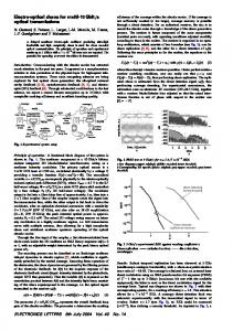
Fig.1 shows the result of the computation for optical absorption with different AD layer thicknesses. The increasing of the AD layer thickness up to 30 nm (6,12% for λ=980 nm) gives the amplitude reduction of absorption maxima more than 0.3 a.u. and leads to red shift of both observed peaks. This effect appears due to the changes in reflection and transmission spectra. With the increasing of the AD layer thickness the transmission spectrum does not change very much. Consequently, for that spectral region the changes of the absorption depend on the reflectivity changes. While the increasing of the thickness, the cavity resonance shifts and the corresponding minimum of reflectance shifts too.
0,02
Optical absorption (a.u.)
2 3
0.8
4
0.6 0.4 0.2 0
975
980
985
Wavelength (nm)
990
995
-0,02 970
0.7
0.1
Reflectivity, a.u.
Quantum efficiency (a.u. )
0.8
0.2
990
995
Optical absorption and quantum efficiency spectra calculation for InGaAs/GaAs RCE PD with AD layer inserted in the top mirror was made by transfer matrix method and energy conservation conception. Compensation of the phase variation of total phase is due to abnormal change of the reflection phase shift near the resonance. It has been shown that QE and absorption depends on thickness of the AD layer and it’s position. The increasing of the AD layer thickness to 30 nm (6,12% for λ=980 nm) gives the amplitude reduction of absorption maxima 0.3 a.u. With values q=1.5, p=11 design with a maximum QE of 92.5% and 6 nm flattop width are presented. REFERENCES
0.9
0.3
980 985 Wavelength (nm)
Fig. 3 – Reflection phase shift versus wavelength in RCE PD with AD DBR at p = 11, q = 1.5.
1
0.4
975
V. CONCLUSIONS
It is important to note that the decreasing of the thickness leads to the blue shift. The shape of the absorption curves is not symmetric to the red shift due to the difference in the transmission which is higher while thickness became < λ/2. For the In0.2Ga0.8As/GaAs structure the flat band voltage equals 2.1 V. Result showed on Fig.2 was obtained at bias = -2 V and ηb= 0.97. Figure 2 presents QE(η) wavelength dependence in RCE PD. Curves corresponds to the different p and q. p and q are the numbers of Al0.65Ga0.35As/GaAs pairs and must satisfy p>q [3]. The main resonator and the resonator formed by AD layer has reflection minimum on the different wavelength. Adding more
0.5
0
-0,01
Fig 1. – Thickness of AD layer: 1- λ/2, 2-λ/2+10 nm, 3-λ/2+20 nm, 4λ/2+30 nm
0.6
0,01
layers to the top mirror (means increasing q) lead to narrowing bandwidth of the AD resonator. This effect provides increasing of the reflection between two cavity modes and decreasing the QE as a result. Figure 3 presents wavelength dependence of reflection phase shift in RCE PD with AD DBR. The reflection phase of the whole structure changes abnormal near to a both resonances in structure. The flat-toped QE critically depends from the shape of the reflection phase curve in this region which has been described earlier [3,5]. The data showed on Figure 3 corresponds to a solid curve on the Figure 2.
1 1
Phase (rad)
IV. RESULTS
1
0.5
0 970
980
Wavelength, nm
990
972 974 976 978 980 982 984 986 988 990 Wavelength (nm)
Fig. 2 – Quantum efficiency spectrum. Solid curve corresponds to q=1.5, p=11. Dashed and dotted corresponds to q=2.5 and q=3.5 respectively.
[1.] M.S. Unlu, S.Strite, "Resonant Cavity enhanced photonic devices," J. Appl. Phys. 1995, Vol. 78, № 2, pp. 607–639. [2.] K.Liu, Y.Huang, X.Ren, "Theory and experiments of a three-cavity wavelength-selective photodetector," Applied Optics, 2000, Vol. 39, № 24, pp. 4263–4269. [3.] C.-H.Chen, K.Tetz, Y.Fainman, "Resonant-cavity-enhanced p-i-n photodiode with a broad quantum-efficiency spectrum by use of an anomalous-dispersion mirror," Applied Optics, 2005, Vol. 44, № 29, pp. 6131–6140. [4.] I-S. Chung, Y. T.Lee, "A method to tune the cavity-mode wavelength of resonant cavity-enhanced photodetectors for bidirectional optical interconnects," IEEE Photonics Technology Letters, 2006, Vol. 18, № 1, pp. 46–48. [5.] Gryshchenko S.V., Dyomin A.A., Lysak V.V., Sukhoivanov I.A. Proceeding of the “Optics and high technology material science” conference”, P. 125, October 2006.
78