Vol. 26, No. 18 | 3 Sep 2018 | OPTICS EXPRESS A750
Optical design of spectrally selective interlayers for perovskite/silicon heterojunction tandem solar cells K. BITTKAU,1,* T. KIRCHARTZ,1,2 AND U. RAU1 1
IEK5 – Photovoltaik, Forschungszentrum Jülich GmbH, 52425 Jülich, Germany Faculty of Engineering and CENIDE, University of Duisburg−Essen, Carl-Benz-Straße 199, 47057 Duisburg, Germany *
[email protected] 2
Abstract: Monolithic perovskite/c-Si tandem solar cells have the potential to exceed the Shockley-Queisser limit for single junction solar cells. However, reflection losses at internal interfaces play a crucial role for the overall efficiency of the tandem devices. Significant reflection losses are caused by the charge selective contacts which have a significantly lower refractive index compared to the absorber materials. Here, we present an approach to overcome a significant part of these reflection losses by introducing a multilayer stack between the top and bottom cell which shows spectrally selective transmission/reflection behavior. The layer stack is designed and optimized by optical simulations using transfer matrix method and a genetic algorithm. The incident sun light is split into a direct part and an isotropic diffuse part. The tandem solar cell with interlayer shows an absolute improvement of short-circuit current density of 0.82 mA/cm2. © 2018 Optical Society of America under the terms of the OSA Open Access Publishing Agreement OCIS codes: (310.4165) Multilayer design; (310.6805) Theory and design; (230.1480) Bragg reflectors; (350.6050) Solar energy.
References and links 1.
J. H. Heo, S. H. Im, J. H. Noh, T. N. Mandal, C. S. Lim, J. A. Chang, Y. H. Lee, H. J. Kim, A. Sarkar, M. K. Nazeeruddin, M. Grätzel, and S. I. Seok, “Efficient Inorganic-Organic Hybrid Heterojunction Solar Cells Containing Perovskite Compound and Polymeric Hole Conductors,” Nat. Photonics 7(6), 486–491 (2013). 2. H. S. Kim, C. R. Lee, J. H. Im, K. B. Lee, T. Moehl, A. Marchioro, S. J. Moon, R. Humphry-Baker, J. H. Yum, J. E. Moser, M. Grätzel, and N. G. Park, “Lead Iodide Perovskite Sensitized All-Solid-State Submicron Thin Film Mesoscopic Solar Cell With Efficiency Exceeding 9%,” Sci. Rep. 2(1), 591 (2012). 3. M. M. Lee, J. Teuscher, T. Miyasaka, T. N. Murakami, and H. J. Snaith, “Efficient Hybrid Solar Cells Based on Meso-Superstructured Organometal Halide Perovskites,” Science 338(6107), 643–647 (2012). 4. W. S. Yang, J. H. Noh, N. J. Jeon, Y. C. Kim, S. Ryu, J. Seo, and S. I. Seok, “High-performance photovoltaic perovskite layers fabricated through intramolecular exchange,” Science 348(6240), 1234–1237 (2015). 5. T. P. White, N. N. Lal, and K. R. Catchpole, “Tandem Solar Cells Based on High-Efficiency c-Si Bottom Cells: Top Cell Requirements for >30% Efficiency,” IEEE J. Photovolt. 4(1), 208–214 (2014). 6. N. N. Lal, T. P. White, and K. R. Catchpole, “Optics and Light Trapping for Tandem Solar Cells on Silicon,” IEEE J. Photovolt. 4(6), 1380–1386 (2014). 7. K. A. Bush, A. F. Palmstrom, Z. J. Yu, M. Boccard, R. Cheacharoen, J. P. Mailoa, D. P. McMeekin, R. L. Z. Hoye, C. D. Bailie, T. Leijtens, I. M. Peters, M. C. Minichetti, N. Rolston, R. Prasanna, S. Sofia, D. Harwood, W. Ma, F. Moghadam, H. J. Snaith, T. Buonassisi, Z. C. Holman, S. F. Bent, and M. D. McGehee, “23.6%efficient monolithic perovskite/silicon tandem solar cells with improved stability,” Nat. Energy 2(4), 17009 (2017). 8. S. Albrecht, M. Saliba, J. P. Correa-Baena, F. Lang, K. Kegelmann, M. Mews, L. Steier, A. Abate, J. Rappich, L. Korte, R. Schlatmann, M. K. Nazeeruddin, A. Hagfeldt, M. Grätzel, and B. Rech, “Monolithic Perovskite/Silicon-Heterojunction Tandem Solar Cells Processed at Low Temperature,” Energy Environ. Sci. 9(1), 81–88 (2016). 9. J. P. Mailoa, C. D. Bailie, E. C. Johlin, E. T. Hoke, A. J. Akey, W. H. Nguyen, M. D. McGehee, and T. Buonassisi, “2-Terminal Perovskite/Silicon Multijunction Solar Cell Enabled by a Silicon Tunnel Junction,” Appl. Phys. Lett. 106(12), 121105 (2015). 10. K. Yoshikawa, H. Kawasaki, W. Yoshida, T. Irie, K. Konishi, K. Nakano, T. Uto, D. Adachi, M. Kanematsu, H. Uzu, and K. Yamamoto, “Silicon heterojunction solar cell with interdigitated back contacts for a photoconversion efficiency over 26%,” Nat. Energy 2(5), 17032 (2017).
#327732 Journal © 2018
https://doi.org/10.1364/OE.26.00A750 Received 5 Apr 2018; revised 24 May 2018; accepted 7 Jun 2018; published 24 Jul 2018
Vol. 26, No. 18 | 3 Sep 2018 | OPTICS EXPRESS A751
11. M. Taguchi, A. Yano, S. Tohoda, K. Matsuyama, Y. Nakamura, T. Nishiwaki, K. Fujita, and E. Maruyama, “24.7% Record Efficiency HIT Solar Cell on Thin Silicon Wafer,” IEEE J. Photovolt. 4(1), 96–99 (2014). 12. S. D. Stranks and H. J. Snaith, “Metal-halide perovskites for photovoltaic and light-emitting devices,” Nat. Nanotechnol. 10(5), 391–402 (2015). 13. L. K. Ono, E. J. Juarez-Perez, and Y. Qi, “Progress on Perovskite Materials and Solar Cells with Mixed Cations and Halide Anions,” ACS Appl. Mater. Interfaces 9(36), 30197–30246 (2017). 14. W. Zhang, G. E. Eperon, and H. J. Snaith, “Metal halide perovskites for energy applications,” Nat. Energy 1(6), 16048 (2016). 15. D. T. Grant, K. R. Catchpole, K. J. Weber, and T. P. White, “Design guidelines for perovskite/silicon 2-terminal tandem solar cells: an optical study,” Opt. Express 24(22), A1454–A1470 (2016). 16. Y. M. Yang, Q. Chen, Y. T. Hsieh, T. B. Song, N. D. Marco, H. Zhou, and Y. Yang, “Multilayer Transparent Top Electrode for Solution Processed Perovskite/Cu(In,Ga)(Se,S)2 Four Terminal Tandem Solar Cells,” ACS Nano 9(7), 7714–7721 (2015). 17. Y. Jiang, I. Almansouri, S. Huang, T. Young, Y. Li, Y. Peng, Q. Hou, L. Spiccia, U. Bach, Y. Cheng, M. A. Green, and A. Ho-Baillie, “Optical analysis of perovskite/silicon tandem solar cells,” J. Mater. Chem. C Mater. Opt. Electron. Devices 4(24), 5679–5689 (2016). 18. G. E. Eperon, M. T. Hörantner, and H. J. Snaith, “Metal halide perovskite tandem and multiple-junction photovoltaics,” Nat. Rev. Chem. 1(12), 0095 (2017). 19. M. T. Hörantner and H. J. Snaith, “Predicting and optimising the energy yield of perovskite-on-silicon tandem solar cells under real world conditions,” Energy Environ. Sci. 10(9), 1983–1993 (2017). 20. G. W. P. Adhyaksa, E. Johlin, and E. C. Garnett, “Nanoscale Back Contact Perovskite Solar Cell Design for Improved Tandem Efficiency,” Nano Lett. 17(9), 5206–5212 (2017). 21. C. D. Bailie and M. D. McGehee, “High-efficiency tandem perovskite solar cells,” MRS Bull. 40(08), 681–686 (2015). 22. M. Jaysankar, W. Qiu, M. van Eerden, T. Aernouts, R. Gehlhaar, M. Debucquoy, U. W. Paetzold, and J. Poortmans, “Four-Terminal Perovskite/Silicon Multijunction Solar Modules,” Adv. Energy Mater. 7(15), 1602807 (2017). 23. M. Filipič, P. Löper, B. Niesen, S. De Wolf, J. Krč, C. Ballif, and M. Topič, “CH3NH3PbI3 perovskite / silicon tandem solar cells: characterization based optical simulations,” Opt. Express 23(7), A263–A278 (2015). 24. S. Albrecht, M. Saliba, J. Correa-Baena, K. Jäger, L. Korte, A. Hagfeldt, M. Grätzel, and B. Rech, “Towards optical optimization of planar monolithic perovskite/silicon-heterojunction tandem solar cells,” J. Opt. 18(6), 064012 (2016). 25. J. Pla, M. Tamasi, R. Rizzoli, M. Losurdo, E. Centurioni, C. Summonte, and F. Rubinelli, “Optimization of ITO layers for applications in a-Si/c-Si heterojunction solar cells,” Thin Solid Films 425(1-2), 185–192 (2003). 26. Z. C. Holman, M. Filipič, A. Descoeudres, S. De Wolf, F. Smole, M. Topič, and C. Ballif, “Infrared light management in high-efficiency silicon heterojunction and rear-passivated solar cells,” J. Appl. Phys. 113(1), 013107 (2013). 27. A. Hoffmann, K. Bittkau, C. Zhang, M. Meier, R. Carius, and U. Rau, “Photon Tunneling in Tandem Solar Cells With Intermediate Reflector,” IEEE J. Photovolt. 6(3), 597–603 (2016). 28. A. Bielawny, C. Rockstuhl, F. Lederer, and R. B. Wehrspohn, “Intermediate reflectors for enhanced top cell performance in photovoltaic thin-film tandem cells,” Opt. Express 17(10), 8439–8446 (2009). 29. P. G. O’Brien, A. Chutinan, K. Leong, N. P. Kherani, G. A. Ozin, and S. Zukotynski, “Photonic crystal intermediate reflectors for micromorph solar cells: A comparative study,” Opt. Express 18(5), 4478–4490 (2010). 30. V. M. Emelyanov, N. A. Kalyuzhnyy, S. A. Mintairov, M. Z. Shvarts, and V. M. Lantratov, “Multijunction GaInP/GaInAs/Ge Solar Cells with Bragg Reflectors,” Semiconductors 44(12), 1600–1605 (2010). 31. A. Mellor, N. P. Hylton, S. A. Maier, and N. Ekins-Daukes, “Interstitial light-trapping design for multi-junction solar cells,” Sol. Energy Mater. Sol. Cells 159, 212–218 (2017). 32. A. Hoffmann, U. W. Paetzold, C. Zhang, T. Merdzhanova, A. Lambertz, C. Ulbrich, K. Bittkau, and U. Rau, “Advancing tandem solar cells by spectrally selective multilayer intermediate reflectors,” Opt. Express 22(S5 Suppl 5), A1270–A1277 (2014). 33. P. Buehlmann, J. Bailat, D. Dominé, A. Billet, F. Meillaud, A. Feltrin, and C. Ballif, “In situ silicon oxide based intermediate reflector for thin–film silicon micromorph solar cells,” Appl. Phys. Lett. 91(14), 143505 (2007). 34. A. Lambertz, T. Grundler, and F. Finger, “Hydrogenated amorphous silicon oxide containing a microcrystalline silicon phase and usage as an intermediate reflector in thin–film silicon solar cells,” J. Appl. Phys. 109(11), 113109 (2011). 35. A. Richter, V. Smirnov, A. Lambertz, K. Nomoto, K. Welter, and K. Ding, “Versatility of doped nanocrystalline silicon oxide for applications in silicon thin-film and heterojunction solar cells,” Sol. Energy Mater. Sol. Cells 174, 96–201 (2018). 36. Y. Wu, D. Yan, J. Peng, T. Duong, Y. Wan, S. P. Phang, H. Shen, N. Wu, C. Barugkin, X. Fu, S. Surve, D. Grant, D. Walter, T. P. White, K. R. Catchpole, and K. J. Weber, “Monolithic perovskite/silicon-homojunction tandem solar cell with over 22% efficiency,” Energy Environ. Sci. 10(11), 2472–2479 (2017). 37. P. S. C. Schulze, A. J. Bett, K. Winkler, A. Hinsch, S. Lee, S. Mastroianni, L. E. Mundt, M. Mundus, U. Würfel, S. W. Glunz, M. Hermle, and J. C. Goldschmidt, “Novel Low-Temperature Process for Perovskite Solar Cells with a Mesoporous TiO2 Scaffold,” ACS Appl. Mater. Interfaces 9(36), 30567–30574 (2017).
Vol. 26, No. 18 | 3 Sep 2018 | OPTICS EXPRESS A752
38. H. Tan, A. Jain, O. Voznyy, X. Lan, F. P. García de Arquer, J. Z. Fan, R. Quintero-Bermudez, M. Yuan, B. Zhang, Y. Zhao, F. Fan, P. Li, L. N. Quan, Y. Zhao, Z.-H. Lu, Z. Yang, S. Hoogland, and E. H. Sargent, “Efficient and stable solution-processed planar perovskite solar cells via contact passivation,” Science 355(6326), 722–726 (2017). 39. J. H. Kim, P. W. Liang, S. T. Williams, N. Cho, C. C. Chueh, M. S. Glaz, D. S. Ginger, and A. K.-Y. Jen, “HighPerformance and Environmentally Stable Planar Heterojunction Perovskite Solar Cells Based on a SolutionProcessed Copper-Doped Nickel Oxide Hole-Transporting Layer,” Adv. Mater. 27(4), 695–701 (2015). 40. M. Saliba, T. Matsui, J.-Y. Seo, K. Domanski, J.-P. Correa-Baena, M. K. Nazeeruddin, S. M. Zakeeruddin, W. Tress, A. Abate, A. Hagfeldt, and M. Grätzel, “Cesium-containing triple cation perovskite solar cells: improved stability, reproducibility and high efficiency,” Energy Environ. Sci. 9(6), 1989–1997 (2016). 41. S. J. Byrnes, “Multilayer optical calculations,” https://arxiv.org/abs/1603.02720. 42. P. B. Johnson and R. W. Christy, “Optical Constants of the Noble Metals,” Phys. Rev. B 6(12), 4370–4379 (1972). 43. G. E. Jellison, Jr., “Optical functions of silicon determined by two-channel polarization modulation ellipsometry,” Opt. Mater. 1(1), 41–47 (1992). 44. R. Perez, R. Stewart, C. Arbogast, R. Seals, and J. Scott, “An anisotropic hourly diffuse radiation model for sloping surfaces: description, performance validation, site dependency evaluation,” Sol. Energy 36(6), 481–497 (1986). 45. P. G. Loutzenhiser, H. Manz, C. Felsmann, P. A. Strachan, T. Frank, and G. M. Maxwell, “Empirical validation of models to compute solar irradiance on inclined surfaces for building energy simulation,” Sol. Energy 81(2), 254–267 (2007). 46. R. L. Haupt and S. E. Haupt, Practical Genetic Algorithms, 2nd Edition (John Wiley & Sons, Inc, 2004). 47. L. Mazzarella, M. Werth, K. Jäger, M. Jošt, L. Korte, S. Albrecht, R. Schlatmann, and B. Stannowski, “Infrared photocurrent management in monolithic perovskite/silicon heterojunction tandem solar cells by using a nanocrystalline silicon oxide interlayer,” Opt. Express 26(10), A487–A497 (2018). 48. B. C. Duck, R. B. Dunbar, O. Lee, K. F. Anderson, T. W. Jones, G. J. Wilson, and C. J. Fell, “Energy Yield Potential of Perovskite-Silicon Tandem Devices,” in 43rd IEEE Photovoltaic Specialists Conference (PVSC) (2016), pp. 1624–1629. 49. R. Santbergen, R. Mishima, T. Meguro, M. Hino, H. Uzu, J. Blanker, K. Yamamoto, and M. Zeman, “Minimizing optical losses in monolithic perovskite/c-Si tandem solar cells with a flat top cell,” Opt. Express 24(18), A1288–A1299 (2016).
1. Introduction The rapid increase in power conversion efficiency of metal halide perovskite solar cells (PSC) [1–4] and their high optical band-gap make these devices to attractive candidates for top cells for crystalline silicon (c-Si) solar cell technology [5–9]. Silicon heterojunction (SHJ) solar cells show very high efficiencies, even higher than silicon homojunction solar cells [10,11]. Recently, many different process technologies and layer combinations were investigated for PSC as this technology still needs much work in order to optimize the device performance [12–14]. In particular, a lot of research is currently ongoing to identify optimal electron and hole transport layers [15–17]. When looking for a tandem cell application, one has to distinguish between monolithic two-terminal devices and four-terminal devices [17–23]. The big advantage of the twoterminal device is that only one matching box is necessary for the module application. In contrast, the four-terminal device allows that both cells can be individually driven at their respective maximum power point, whereas current matching has to be taken into account for the two-terminal concept. From an optical point of view, one has to take care about any layer between the top cell absorber and the bottom cell absorber for both tandem device concepts to achieve a good optical matching. In particular, layers with refractive indices significantly lower than those of the absorber layers cause reflection losses for light with photon energies lower than the band gap of the top cell absorber [15,23,24]. In case of the four-terminal architecture, two contact layers with sufficiently low sheet resistance need to be deposited between the top cell and bottom cell absorber in order to collect the charge carriers from both cells. Such layers typically show significant absorption losses. Additionally, the mechanical stacking demands for a transparent medium like glass, air or an index matching liquid which separates these contact layers. Therefore, an optically thick region with low refractive index and high absorption can hardly be avoided here.
Vol. 26, No. 18 | 3 Sep 2018 | OPTICS EXPRESS A753
The two-teerminal architeecture offers a big advantage.. For SHJ solarr cells, indium tin oxide (ITO) layers were common nly applied at the t front contaact due to theiir good combiination of d optical propeerties [25,26]. Although ITO O as well as ccommonly useed charge electrical and selective con ntacts for thee PSC still exhibit e low rrefractive inddices, such laayers are comparatively y thin, in particcular in the casse of a tandem device, where lateral charge transport is not required. Therefore, the t optical ligh ht coupling bettween top and bottom cell iss possible oherent light co oupling [27]. This T allows the design of phottonic layer archhitectures in terms of co which partly compensate c refflection losses of impinging llight [28–32]. In this pap per, we presen nt the optical design d of a speectrally selectivve interlayer ((IL) stack based on hydrrogenated micrrocrystalline siilicon oxide (µ µc-SiOx:H) layeers with variouus oxygen contents whicch form a reduced dielectric Bragg B reflectoor that is sandw wiched betweenn top and bottom cell [32–34]. [ It wiill be shown that t without thhis layer stackk, the reflectioon losses dominantly occur o in a restricted spectraal range. The introduction oof the IL signnificantly reduces the ov verall reflection losses. We will w demonstratte that the shorrt-circuit currennt density (JSC) of a two o-terminal PSC C/SHJ tandem solar cell cann be increased by 0.82 mA/ccm2 when applying our IL. This valuee is 0.18 mA//cm2 higher coompared to thee optimized laayer stack SiOx:H interlay yer due to impproved spectrall matching bettween top including justt a single µc-S and bottom ceell. Our study includes a cov ver glass on topp of the tandem m cell and acccounts for ambient light illumination in ncluding the diiffusive part off incident sun llight. We will sshow that olar cell includ ding the IL outp performs the rreference tandeem solar cell w without IL the tandem so for any angle of incident sun n light. 2. Methodollogy 2.1 Device structure s
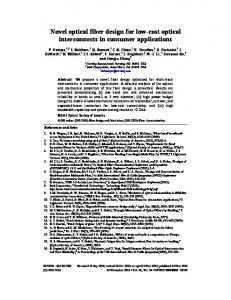
Fig. 1. 1 Illustration of th he layer stack used d for the study. T Thicknesses were pprovided for thosee layerss, where the thickn ness was not varied during the opti timization proceduure. The arrows att the to op illustrate the asssumed incident sun s light with AM M1.5d at normal incidence and thee isotropic impinging difffuse part of the AM M1.5g.
We focus ourr study to SHJJ bottom solar cells applyingg hydrogenatedd amorphous ssilicon (aSi:H) passivaation layers and d doped hydro ogenated, nanoocrystalline siliicon oxide (ncc-SiOx:H) charge carrierr selective conttacts as such laayers have a hiigh optical trannsparency andd the solar cells reveal reasonably hiigh efficienciees [35]. As the a-Si:H laayers are lim miting the f any further deposition process, p any m material whichh requires tem mperatures temperature for higher than 200 2 °C is no op ption for the PSC. P As one eexample, the coommonly usedd TiOx as
Vol. 26, No. 18 | 3 Sep 2018 | OPTICS EXPRESS A754
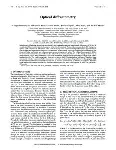
electron transport layer for PSC is often annealed at temperatures of 400 °C [36], although lower process temperatures were reported [37,38]. Besides other possible materials that do not require such high temperatures, Poly(3,4-ethylenedioxythiophene):poly(styrenesulfonate) (PEDOT:PSS) is used as hole transport layer for our simulation study as the processing is simple and flexible, resulting in reasonable efficiencies [39]. As electron transport layer, we use [6,6]-phenyl-C61-butyric acid methyl ester (PCBM). The whole layer stack is illustrated in Fig. 1. As back reflector, an 80 nm thick aluminum doped zinc oxide (ZnO:Al) and a 500 nm thick silver (Ag) layer stack is assumed. The c-Si absorber is passivated at both sides with 5 nm thick a-Si:H. 30 nm thick p-doped and n-doped nc-SiOx:H was assumed at the back and front side of the 250 µm thick silicon wafer as carrier selective contact layers for the bottom cell, respectively. The bottom cell is complemented with an ITO layer. The IL consists of three µc-SiOx:H layers with high, low and high refractive index, respectively. For the top cell, PEDOT:PSS is assumed as hole transport layer, followed by a quadruple cation perovskite layer with a bandgap energy of 1.65 eV, which can be prepared similar to a previously published recipe [40] with added guanidinium iodide. Details about this process will be published elsewhere. The perovskite layer is coated with a 20 nm thick PCBM as electron transport layer, capped with a buffer layer consisting of ZnO nanoparticles (ZnO NP) and a 700 µm thick glass cover sheet. During the study, the thicknesses of the ITO, the individual layers of the IL, the PEDOT:PSS, the perovskite and the ZnO NP were varied in order to achieve the highest possible JSC. All interfaces were assumed to be flat. 2.2 Simulation The optical design of the layer stack is done based on the transfer matrix method (TMM) [41]. The complex refractive indices for Ag and c-Si were taken from literature [42,43]. The values for all other materials were experimentally determined by a combination of reflection/transmission measurement, spectroscopic ellipsometry and photo-thermal deflection spectroscopy on reference samples. All layers with silicon and silicon-based alloys were deposited by plasma enhanced chemical vapor deposition, ITO and back contact by sputtering and the layers of the top solar cell by spin coating from liquid phase. For the most important layers for the optical matching condition between top cell and bottom cell, the wavelength dependent refractive indices n (a) and extinction coefficients k (b) were shown in Fig. 2. The wavelength of 750 nm is depicted as dotted vertical line. This wavelength almost equals the optical bandgap of the perovskite layer and, therefore, represents the spectral region where the optical matching between top and bottom cell is mostly relevant. At this wavelength, the two absorber layers have the highest refractive indices n (3.71 for c-Si and 2.44 for perovskite) with respect to the other materials, whereas the two layers that extract the charge carriers, PEDOT:PSS and ITO, have the lowest refractive indices (1.54 and 1.71, respectively). As interlayers, the high refractive silicon oxide alloy with lower oxygen content and a refractive index of 2.17 at a wavelength of 750 nm was assumed. The second component of the IL consists of a µc-SiOx:H with higher oxygen content and, therefore, lower refractive index of 1.77 at a wavelength of 750 nm.
Vol. 26, No. 18 | 3 Sep 2018 | OPTICS EXPRESS A755
Fig. 2. (a) Refractive index n and (b) extinction coefficient k for the most relevant materials for the optical matching condition between top and bottom cell. The vertical dotted lines depict the wavelength which corresponds to the optical bandgap of the perovskite.
For the TMM simulation, the 700 µm thick glass sheet as well as the 250 µm thick c-Si were assumed as incoherent layers, whereas all other layers were assumed as coherent layers. As the illumination conditions are of major importance for tandem solar cells, the incident light is assumed to consist of a direct and a diffusive component. For the direct light, the AM1.5d spectrum is assumed to impinge along the surface normal. The diffuse part of the sun light (AM1.5g-AM1.5d) is spread over nine angles of incidence, 0°-80° in steps of 10°. The intensities for each angle were weighted in a way to assume an isotropic illumination characteristic from the upper half space. This illumination and the glass cover sheet were chosen to represent a much more realistic condition for real application compared to common approaches. More advanced sky models split the sky into a circumsolar region, a near-horizon region and the remaining region. Although those models describe the solar irradiance more accurately compared to the isotropic assumption [44,45], the deviations are small compared to regional variations of the sun spectrum and the impact of mounting angles on the incident solid angle range. The absorptance in each layer was extracted and the corresponding JSC of the tandem solar cell calculated from the minimum of the charge carrier generation in both absorber layers. By applying a genetic algorithm [46], the layer thicknesses were optimized to achieve the maximal JSC. The advantages of a genetic algorithm are its ability to deal with multiple variables and its applicability to parallel processing. Furthermore, a genetic algorithm does not need derivative information for optimization. The population size,
Vol. 26, No. 18 | 3 Sep 2018 | OPTICS EXPRESS A756
selection fraction, mutation rate and number of iterations were chosen to be 450, 0.65, 0.08 and 400, respectively, and the generated JSC is taken as fitness value. For the ZnO NP, PEDOT:PSS and ITO layers, lower boundaries for the thickness were defined as 35 nm, 20 nm and 35 nm, respectively. 3. Results and discussions This section is structured as follows. First, we present an optical loss analysis for the optimized reference tandem solar cell without IL stack. We will demonstrate that reflection losses in the spectral range from 600 nm – 900 nm play a major role in the limitation of the device. Next, we will introduce the three-layer stack as IL between the top and bottom cell. We will demonstrate that this IL3 causes a significant reduction of reflection losses which increases the absorptance in both, top cell and bottom cell absorber. This will be complemented by a direct comparison of absorptance and solar cell reflectance for the layer stacks with and without IL. For comparison, we also designed a tandem solar cell with a single IL1 [47] consisting of the µc-SiOx:H layer with higher refractive index. Our study will be finalized by a quantification of the effect of the IL3 on the JSC as a function of the angle of incidence. Table 1. Layer thicknesses resulting from the optimization of the tandem solar cell without and with IL interlayer without with IL1 with IL3
ITO 35 nm 35 nm 36 nm
IL1 NA 99 nm 57 nm
IL2 NA NA 128 nm
IL3 NA NA 95 nm
PEDOT:PSS 26 nm 35 nm 21 nm
perovskite 220 nm 251 nm 256 nm
ZnO NP 35 nm 41 nm 36 nm
Table 1 summarizes the layer thicknesses that were determined by the optimization procedure of the genetic algorithm for the tandem solar cell without and with IL. The order of the columns follows the order of the layers in the tandem solar cell stack in the direction from the bottom cell to the front contact. IL1 and IL3 represent the high refractive µc-SiOx:H, IL2 shows the thickness of the low refractive µc-SiOx:H layer. Note that the optimized thicknesses for the ITO, PEDOT:PSS and ZnO NP layers were very close to the lower boundaries of 35 nm, 20 nm and 35 nm, respectively. Figure 3(a) shows the optical loss analysis for the tandem solar cell stack without IL. Any colored area corresponds to the amount of incident light that is absorbed in the related layer. The top and bottom cell absorber, perovskite and c-Si, were represented by the black and red color, respectively. The absorptance in the ZnO NP and PCBM layers at the front side of the tandem solar cell were shown in magenta and green, respectively. PEDOT:PSS is shown as dark blue and ITO as light blue area. The optical losses within the passivation and charge carrier selective contacts of the SHJ bottom cell were represented together in orange. The absorptance in the back reflector stack (ZnO:Al/Ag) is shown in dark yellow. The white area corresponds to light that is reflected by the whole tandem solar cell stack. Only the black and red areas correspond to the JSC. Any other colored area contributes to parasitic absorption losses. The parasitic absorption in the short-wavelength range (wavelengths λ600 nm, the main contribution to the parasitic absorption is given by the absorption losses in the PEDOT:PSS layer (1.13 mA/cm2) followed by ITO (0.67 mA/cm2). Absorption losses originating from other layers are negligible. A huge contribution to optical losses arises from solar cell reflectance. Reflection losses in the long wavelength range (λ>1000 nm) can hardly be avoided with the assumed flat interfaces due to the weak absorption in both absorber layers. A remarkable reflection loss occurs in the spectral range 600 nm