Journal of the Korean Physical Society, Vol. 45, December 2004, pp. S615∼S617
Optical Properties of In-Rich InGaN/GaN Single Quantum Well Structures with High Density of Clusters Yuanping Sun and Yong-Hoon Cho∗ Department of Physics and Institute for Basic Science Research, Chungbuk National University, Cheongju 361-763
Hwa-Mok Kim and T. W. Kang Quantum-functional Semiconductor Research Center, Dongguk University, Seoul 100-715
S.-Y. Kwon and Euijoon Yoon School of Materials Science and Engineering, Seoul National University, Seoul 151-742 An In-rich InGaN/GaN single quantum well structure has been successfully grown by metalorganic chemical vapor deposition. Optical properties were systematically studied by photoluminescence (PL), PL excitation (PLE), selective excitation PL and cathodoluminescence (CL). The PL intensity of the In-rich InGaN structure decreased only by a factor of 17.7 when the temperature increased from 10 K to 300 K, showing a high quantum efficiency. Two different InGaN-related emissions and absorption-edges have been verified by selective excitation PL and PLE. CL observation showed that the epilayer agglomerated together to form clusters due to the large lattice and thermal mismatch and that the two different InGaN emissions originated from spatially different regions. PACS numbers: 78.55.Cr, 78.60.Hk, 78.66.Fd, 81.15.Gh Keywords: In-rich InGaN/GaN single quantum well, Optical properties, Clusters, Metalorganic chemical vapor deposition
I. INTRODUCTION
For the last decade, the III-nitride semiconductor materials have been viewed as the most promising materials for device applications [1–3] between ultraviolet (AlN : 6.2 eV) and infrared (InN : 0.7 eV [4,5]). GaN, AlN, InN, and their ternary (AlGaN, InGaN, etc.) and quarternary (AlInGaN) alloys make up of the most active fields in recent semiconductor researches. As compared to the other III-nitride semiconductors, InN is rarely investigated because of the thermal instability of InN as well as the large lattice and thermal mismatch, which makes it very difficult to grow high quality epilayers. Recently, some advances have been reported for the growth of Inrich InGaN/GaN single quantum well (SQW) structures by adopting growth interruption [6, 7]. In this paper, we report the optical properties of the In-rich InGaN/ GaN single quantum well structures with high density of clusters. II. EXPERIMENT ∗ E-mail:
[email protected]
In-rich InGaN/GaN SQW structures were grown on the c-axis sapphire substrate by metalorganic chemical vapor deposition (MOCVD). The growth pressure was maintained at 300 Torr throughout the whole process. The In-rich InGaN layer was grown for 90 s at 730 ◦ C on a 2-µm-thick GaN epilayer, followed by a 20-nm-thick GaN capping layer grown at 730 ◦ C. No growth interruption was introduced between the In-rich InGaN and GaN capping layers. For comparison, another sample was grown under the same condition except for the 5-s growth interruption after the growth of InN, resulting in a planar surface. For the effective NH3 cracking at low growth temperatures [8] and the reduction of native defects [9], the ammonia was preheated before it entered the reactor. Although only trimethylindium (TMIn) and ammonia were supplied during the growth of the In-rich InGaN layer, the solid-state intermixing of the InN layer with GaN barrier layers at relatively high growth temperature can not be completely ruled out. Hereafter, the grown layer is referred to as In-rich InGaN layer. The In-rich InGaN/GaN SQW structures were characterized by photoluminescence (PL), PL excitation (PLE) and cathodoluminescence (CL). A He-Cd laser (325 nm) was used for the PL experiments, and a Xe lamp dispersed by a monochromator was used as a pumping source for the
-S615-
-S616-
Journal of the Korean Physical Society, Vol. 45, December 2004
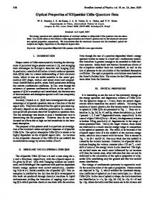
Fig. 1. Temperature-dependent PL measured from 10 K to 300 K by He-Cd laser. The intensity of the main In-rich InGaN peak decreased by a factor of only 17 when the temperature increased from 10 K to 300 K.
Fig. 2. Selective-excitation PL measured at 10 K with a Xe lamp. The excitation energies were set to be higher than GaN (325 nm), higher than DAP (375 nm), and higher than structure main peak P1 (380 nm).
PLE experiments. The CL images were acquired by using a commercial MonoCLT2 M system in a high-resolution scanning electron microscope at 80 K.
III. RESULTS AND DISCUSSION Figure 1 shows the temperature dependent PL data of the In-rich InGaN SQW sample in a temperature range from 10 K to 300 K. Five emission peaks appear at 3.47, 3.28, 3.16, 2.70, and 2.15 eV in the PL spectra at 10 K; these are denoted as GaN, donor-to-acceptor pair (DAP), P1, P2, and yellow band, respectively (to be shown below). The intensity of the main InGaN related peak P1 decreased by a factor of 17.7 with increasing temperature
Fig. 3. PLE data measured at 10 K with Xe lamp dispersed by monochromator. The detection energy was set at 392 nm and 464 nm, which is the emission peak of the two In-rich InGaN structures, respectively.
from 10 K to 300 K, which shows a good quantum efficiency. In comparison, the temperature dependent PL of the sample grown with 5-s interruption showed an intensity decrease of the corresponding peak by a factor of ∼ 4000 with increasing temperature from 10 K to 300 K. Generally, a growth interruption is introduced to smooth the surface of epilayers by decreasing the possibility of the formation of potential fluctuation structures through the adatom migration. However, it is likely that this kind of potential fluctuation is very important for the InGaN structures to improve the quantum efficiency. So, the temperature-dependent PL intensity of the In-rich InGaN structure decreases very fast after introducing the growth interruption because of decreasing of potential fluctuations. Selective excitation on the sample was conducted at 10 K to distinguish the origin of the peaks P1 and P2, with the excitation energy higher than GaN, DAP, and P1 peak, respectively. The results are shown in Figure 2. When the sample was excited with energy lower than GaN and DAP, the P1 and P2 peaks still appear, indicating that the P1 and P2 peaks are not related to GaN. The decrease of the peak intensity with decrease of excitation energy reflects the effect of GaN structure on these two peaks, which was also shown in the PLE results. From the result, we can assign these two emission peaks to In-rich InGaN regions with different indium component. The large energy difference between the P2 peak position and the pure InN (bandgap of InN of ∼ 0.7 eV) can be explained by possible intermixing between InN and GaN layers during the growth and a small well width of the SQW, as estimated by the calculation of Ref. [6]. PLE spectra measured at 392 nm (P1) and 464 nm (P2) at 10 K are shown in Figure 3, together with the PL data excited at a wavelength of 325 nm from a Xe lamp. Clear absorption edges are shown for GaN and
Optical Properties of In-Rich InGaN/GaN Single Quantum Well· · · – Yuanping Sun et al.
-S617-
IV. CONCLUSION We have systematically investigated the optical properties of an In-rich InGaN/GaN single quantum well sample with high density of clusters grown by MOCVD. High efficiency of the emission was found by temperature dependent PL. In-rich InGaN emissions have been verified by selective excitation PL and the different absorption edge of PLE. CL observation showed that the epilayer had agglomerated together to form clusters because of the large lattice and thermal mismatch, which ensure the relatively high quantum efficiency of the samples.
ACKNOWLEDGMENTS
Fig. 4. CL spectra and images acquired by MonoCL2T M system in a high-resolution scanning electron microscope at 80 K with the accelerating voltage of 10 kV. (a) CL spectrum of In-rich InGaN sample; (b) CL images measured at A, B, and C (as denoted in Fig. 4a).
This work was supported by Korea Science and Engineering Foundation through the Quantum-functional Semiconductor Research Center at Dongguk University and by the Program for the Training of Graduate Students in Regional Innovation which was conducted by the Ministry of Commerce, Industry and Energy, and by Nano R&D Program and National Research Laboratory from the Korean Ministry of Science and Technology.
REFERENCES two different indium component In-rich InGaN layers. Large Stokes-like shifts of the In-rich InGaN emissions between the PL peak position and PLE absorption edge are observed. The PLE contribution of the GaN layer to the In-rich InGaN emissions can be clearly seen for both PLE spectra. However, for the PLE spectrum detected at 463.6 nm (P2), no specific PLE feature appears near the P1 peak, reflecting that the channel between the P1 and P2 emissions are not connected each other. Figures 4(a) and 4(b) shows CL spectrum and CL images taken at 356 (A), 389.5 (B), and 452.5 (C) nm, respectively. All the emissions come from the cluster structures. Although the CL emission from GaN covers the full cluster together, the peak B emitted from only the side edge of the cluster and the peak C comes from the central part of the cluster, leading to CL images with reverse contrast. It is likely that the growth of a planar InN layer is very difficult since the epilayer agglomerates together during the deposition of the InN to form the cluster due to the large lattice and thermal mismatch between GaN and InN. The deposition of GaN below and above the InN layer packaged the InN layer inside to form the clusters. More GaN is included in the InN region at the side edge part of the clusters; while the InN region at the central part of the clusters is possessed of less amount of GaN, resulting in the different CL (PL) peaks B (P1) and C (P2).
[1] S. Nakamura and G. Fasol, The blue laser diode (Springer, Berlin, 2000). [2] Le Si Dang, G. Fishman, H. Mariette, C. Adelmann, E. Martinez J. Simon, B. Daudin, E. Monroy, N. Pelekanos, J.L. Rouviere, and Y.H. Cho, J. Korean Phys. Soc. 42, S657 (2003). [3] Y. H. Cho, C. W. Son, and J. Y. Kim, B. M. Kim, W. S. Lee, S. N. Lee, J. K. Son, O. H. Nam, and Y. J. Park, J. Korean Phys. Soc 44, L792 (2004). [4] T. Matsuoka, H. Okamoto, M. Nakao, H. Harima and E. Kurimoto, Appl. Phys. Lett. 81, 1246 (2002). [5] M. Yoshimoto, H. Yamamoto, W. Huang, H. Harima, J. Saraie, A. Chayahara and Y. Horino, Appl. Phys. Lett. 83, 3480 (2003). [6] H. J. Kim, H. Na, S.-Y. Kwon, H. C. Seo, H. J. Kim, Y. Shin, K. H. Lee, Y. W. Kim, S. Yoon, H. J. Oh, C. Sone, Y. Park, Y. H. Cho, Y. Sun and E. Yoon, Phys. Stat. Sol. (c) 0, 2834 (2003). [7] S.-Y. Kwon, H. J. Kim, H. Na, H. C. Seo, H. J. Kim, Y. Shin, Y. W. Kim, S. Yoon, H. J. Oh, C. Sone, Y. Park, Y. Sun, Y. H. Cho and E. Yoon, Phys. Stat. Sol. (c) 0, 2830 (2003). [8] H. J. Kim, S.-Y. Kwon, S. G. Yim, H. Na, B. Kee, E. Yoon, J. Kim, S.-H. Park, H. Jeon, S. Kim, J. H. Seo, K. Park, M. Seon, C. Sone, O. H. Nam, and Y. Park, Current Appl. Phys. 3, 351 (2003). [9] S.-Y. Kwon, H. J. Kim, B. Kee, H. Na and E. Yoon, Phys. Stat. Sol. (c) 0, 405 (2002).