Dec 21, 2011 - grown diamond, and also after electron irradiation and annealing, suggesting the ... The presence of silicon (Si) in diamond has been routinely.
PHYSICAL REVIEW B 84, 245208 (2011)
Optical properties of the neutral silicon split-vacancy center in diamond U. F. S. D’Haenens-Johansson, A. M. Edmonds, B. L. Green, and M. E. Newton* Department of Physics, University of Warwick, Coventry, CV4 7AL, United Kingdom
G. Davies Department of Physics, King’s College London, Strand, London, WC2R 2LS, United Kingdom
P. M. Martineau and R. U. A. Khan DTC Research Centre, Belmont Road, Maidenhead, Berkshire, SL6 6JW, United Kingdom
D. J. Twitchen Element Six Ltd., King’s Ride Park, Ascot, Berkshire, SL5 8BP, United Kingdom (Received 1 March 2011; revised manuscript received 6 November 2011; published 21 December 2011) The zero-phonon line (ZPL) at 1.68 eV has been attributed to the negatively charged silicon split-vacancy center in diamond, (Si-V)− , and has been extensively characterized in the literature. Computational studies have predicted the existence of the neutral charge state of the center, (Si-V)0 , and it has been experimentally observed using electron paramagnetic resonance (EPR). However, the optical spectrum associated with (Si-V)0 has not yet been conclusively identified. In this paper the 1.31 eV band visible in luminescence and absorption is attributed to (Si-V)0 using an approach which combines optical absorption and EPR measurements. The intensities of both 1.68 eV and 1.31 eV bands are found to increase in deliberately Si-doped chemical vapor deposition (CVD) grown diamond, and also after electron irradiation and annealing, suggesting the involvement of both Si and a vacancy in the centers. The 1.31 eV ZPL is unambiguously associated to Si by its shift to a lower energy when the dominant Si isotope is changed from 28 Si to 29 Si. Charge transfer between (Si-V)− and (Si-V)0 induced via ultraviolet photoexcitation or heating in the dark allows calibration factors relating the integrated absorption coefficient of their respective ZPLs to the defect concentration to be determined. Preferential orientation of (Si-V)0 centers in CVD diamond grown on {110}-oriented diamond substrates is observed by EPR. The (Si-V)0 centers are shown to grow predominantly into CVD diamond as complete units, rather than by the migration of mobile vacancies to substitutional Si (SiS ) atoms. Corrections for the preferential alignment of trigonal centers for quantitative analysis of optical spectra are proposed and the effect is used to reveal that the 1.31 eV ZPL arises from a transition between the 3A2g ground state and 3A1u excited state of (Si-V)0 . A simple rate equation model explains the production of (Si-V)0 upon irradiation and annealing of Si-doped CVD diamond. In as-grown Si-doped diamond the (Si-V) defects only account for a fraction of the total silicon present; the majority being incorporated as SiS . The data show that both SiS and (Si-V) are effective traps for mobile vacancies. DOI: 10.1103/PhysRevB.84.245208
PACS number(s): 81.05.ug, 78.40.Fy, 78.55.Ap, 76.30.Mi
I. INTRODUCTION
The presence of silicon (Si) in diamond has been routinely verified by the detection of the 1.68 eV (737 nm) zero-phonon line (ZPL) in luminescence or absorption, which has been attributed to the negatively charged silicon split-vacancy center, (Si-V)− .1,2 Unless preventative measures are taken, Si impurities may be introduced into chemical vapor deposition (CVD) grown diamond as a consequence of plasma etching of Si-containing reactor components.3,4 Intentional Si-doping has been achieved during the growth of both CVD and highpressure, high-temperature (HPHT) synthetic diamond.5,6 The occurrence of (Si-V)− in natural untreated diamond is rare. Of the order of 1 in 1000 gem-quality specimens investigated by a major grading laboratory contain this center.7,8 Therefore, observation of (Si-V)− is frequently used to help distinguish between natural, CVD synthetic or treated diamond.7,8 There has also been interest in (Si-V)− by the quantuminformation community due to its potential use as a single photon source. Single photon detection from color centers in diamond has been achieved using the negatively charged nitrogen-vacancy [(N-V)− ] center,9,10 with its ZPL at 1.945 eV 1098-0121/2011/84(24)/245208(14)
(637 nm), and systems with ZPLs at 1.55 eV (802 nm)11,12 and 1.64 eV (756 nm).13 Most research has been conducted on (N-V)− due to its long coherence time and the relative ease of fabrication.14 However, its broad emission band at room temperature is a disadvantage as it prevents efficient filtering of the background signals.10 Room temperature single photon emission has been observed from (Si-V)− centers in ion implanted type IIa bulk diamond15 and more recently with a much greater quantum efficiency in Si-doped CVD nanodiamonds.16 There are several properties that render (Si-V)− noteworthy for quantum-information applications. (Si-V)− has a remarkably sharp ZPL, with a width of ∼0.7 nm reported at room temperature (to date, the most narrow for a color center in diamond),16 and a weak vibronic sideband characterized by a small Huang-Rhys factor SHR . The values of SHR for the 1.68 eV band of the (Si-V)− center determined from both absorption and photoluminescence measurements cited in the literature range from 0.05 to 0.29.16–19 Furthermore, the centers emit light in a wavelength region where there is low background fluorescence from diamond.16 Recent reports of single photon count rates up to 4.8 × 10⁶ counts/s at saturation for (Si-V)− are significantly higher than those for
245208-1
©2011 American Physical Society
U. F. S. D’HAENENS-JOHANSSON et al.
PHYSICAL REVIEW B 84, 245208 (2011)
(a)
(b)
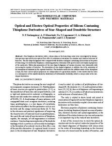
FIG. 1. (Color online) (a) Schematic of the silicon split-vacancy defect in diamond, (Si-V), with the {110} mirror plane highlighted. The silicon atom is illustrated as a large yellow sphere lying halfway between two vacant lattice sites; all other atoms are carbon, with the dangling orbitals shown in blue. The silicon atom is equidistant from six nearest-neighbor carbon atoms. (b) Simple molecular-orbital model for (Si-V): The central silicon atom and ligand orbitals interact, resulting in the molecular orbitals illustrated. The arrows indicate the 10 unpaired electrons available to fill the energy levels for (Si-V)0 .
(N-V)− (∼105 counts/s) and even the 1.64 eV luminescent center (3.2 × 10⁶ counts/s).10,13,16 Electron paramagnetic resonance (EPR) and computational studies have shown the existence of the neutral charge state of the silicon split-vacancy center (Si-V)0 .2,20,21 Although the center has been identified, its optical spectrum has not hitherto been unambiguously determined. The ZPL at 1.31 eV (946 nm) has been previously attributed to (Si-V)0 via a combination of EPR and optical absorption data.22 Additionally, charge transfer was induced between the (Si-V)− and (Si-V)0 centers, enabling the calculation of calibration factors which can be used to determine the concentration of the centers from the integrated absorption coefficients of the ZPLs at 77 K.22 In this paper the optical properties of the 1.31 eV band are investigated in detail and new data are presented supporting the assignment to the (Si-V)0 center. Studies of the production of both the 1.68 eV and 1.31 eV bands by irradiation and annealing is modeled in terms of vacancy capture by substitutional silicon. Grown-in (Si-V)0 centers are shown by EPR to display preferential alignment with respect to the growth plane in homoepitaxial CVD diamond grown on {110}-oriented substrates. The importance of allowing for the preferential alignment of the centers when using optical absorption for quantitative measurements of the concentration of (Si-V)0 is demonstrated. It will be shown (Sec. IV B) that information about the nature of the 1.31 eV band transition can be extracted from measurements on samples in which the defect is preferentially aligned. A. The silicon split-vacancy center in diamond
Spin-polarized local density-functional-cluster theory was employed by Goss et al. to predict that an impurity complex consisting of a substitutional silicon atom next to a vacant lattice site in diamond is unstable.2 The system spontaneously
relaxes into a split-vacancy configuration, with the silicon atom lying in a bond-centered site between two vacancies, with D3d symmetry [Fig. 1(a)]. This configuration is also known as a paired or double semivacancy23 and is consistent with the structure assumed by complexes in diamond which contain vacancies and large dopants, such as cobalt or nickel.24–28 A simple molecular orbital, similar to that used for a tin atom at the center of a divacancy in silicon,29 can be used to interpret the electronic structure of the (Si-V) defect in diamond. The central silicon atom’s 3s and 3p orbitals interact with the ligand orbitals which are formed from a linear combination of a single dangling orbital from each of the six carbon atoms. In D3d symmetry the linear combination of carbon dangling orbitals transform as a1g , a2u , eu , and eg , while those for the silicon 3s and 3p transform as a1g , and a2u and eu , respectively. Figure 1(b) shows that in this model the populated electronic orbitals derive primarily from the “divacancy” ligand orbitals of the six carbon atoms,30 which have been lowered in energy by the presence of the silicon atom. Only a small admixture of silicon character is expected. For (Si-V)0 10 electrons are accommodated in these or2 2 4 2 a2u eu eg [assumbitals. The lowest energy configuration is a1g ing the order of the orbital energy levels shown in Fig. 1(b)]. This one-electron configuration gives rise to 3A2g , 1Eg , and 1 A1g many-electron states. The spin triplet 3A2g state has been assigned to the observed S = 1 ground state of (Si-V)0 , where S is the effective spin.21 Promotion of an electron from eu to eg 2 2 3 3 results in the configuration a1g a2u eu eg , giving rise to the many3 1 3 electron states A1u , A1u , A2u , 1A2u , 3Eu , and 1Eu . Another 2 2 2 4 a2u eu eg configuration and electron promotion results in an a1g 3 1 1 gives rise to A2g , Eg , and A1g many-electron states. We would expect other configurations to be significantly higher in energy. Determining the order of the many-electron states from even the three configurations considered above is a taxing theoretical problem, and this is not attempted here, though
245208-2
OPTICAL PROPERTIES OF THE NEUTRAL SILICON . . .
PHYSICAL REVIEW B 84, 245208 (2011)
TABLE I. Summary of sample properties and treatments. For the samples that were irradiated, each irradiation treatment was followed by annealing according to the tabulated details. Sample A
Sample C
Sample D
Substrate orientation 29 Si abundance 1st treatment
{110} 90% N/A
2nd treatment
N/A
{113} 4.7% 1 × 10¹⁸ 1.5 MeV e− /cm2 + 4 h anneal at 900 ◦ C N/A
1 h at 1200 ◦ C 1 h at 1400 ◦ C 1 h at 1600 ◦ C 2 h at 2000 ◦ C
N/A N/A N/A N/A
{001} 4.7% 1 × 10¹⁷ 1.5 MeV e− /cm2 + 4 h anneal at 900 ◦ C 5 × 10¹⁷ 1.5 MeV e− /cm2 + 4 h anneal at 900 ◦ C N/A N/A N/A N/A
1st anneal 2nd anneal 3rd anneal 4th anneal
possible electron dipole transitions from the 3A2g ground state are considered. For the divacancy system of D3d symmetry the components of the electron dipole operator, which are proportional to x, y, z, transform as follows: z⊂A2u ; x,y⊂Eu . Therefore, the allowed electron dipole transitions from the ground state are 3A2g → 3A1u and 3A2g → 3Eu .30 The fact that the 3A2g → 3A1u and 3A2g → 3Eu transitions have different polarization behavior is crucial later (Sec. IV B) to understand the nonrandom orientations of (Si-V) grown into samples. In the negative charge state (Si-V)− , there are 11 electrons to accommodate, giving rise to the lowest energy configuration 2 2 4 3 a1g a2u eu eg . A 2Eg ground state is expected, and since the promotion of one electron from eu to eg gives rise to the 2Eu state the 1.68 eV optical transition associated with (Si-V)− has been assigned to the 2Eg → 2Eu transition.1,2 The band was shown to consist of a 12-line fine structure by Clark et al.,1 where the 12 lines were divided into three groups of four equally intense lines, whose relative intensities reflected the relative abundance of the silicon isotopes (28 Si, 29 Si, and 30 Si). The multiplicity of the lines was consistent with a transition from an orbitally twofold degenerate ground state, split by 0.20 meV, to a doublet state split by 1.07 meV.1 The splitting of the doublets has been attributed to a (dynamic) Jahn-Teller effect.2 Despite the prediction that (Si-V)− has a paramagnetic ground state with S = 12 ,2,31 it has not yet been unambiguously observed using EPR. II. EXPERIMENTAL DETAILS
A suite of single crystal samples grown homoepitaxially by microwave-assisted CVD on {110}, {001}, and {113}oriented single crystal substrates (samples A, B, and C, respectively) were studied. All samples were intentionally doped with silicon by adding silane to the CVD growth gases; samples A and B were grown with 90% 29 Si-enriched silane (Voltaix USA), whereas samples C and D were grown using silane containing the natural abundance of Si isotopes (28 Si:29 Si:30 Si = 92.3:4.7:3.0). Sample D was grown on a {001}-oriented substrate and during growth the concentration of silicon in the gas phase was adjusted to produce a sample with six layers with progressively higher silicon doping. For samples A, B, and C the substrates were removed to leave free-standing plates, which were cut and polished to eliminate
poor quality material from the edges. A cross-sectional piece of sample D was prepared, allowing the study of the different layers. Sample B was investigated in its as-grown state, while the other samples were treated by irradiation (samples C and D) and annealing (samples A, C, and D). The treatment histories of these samples are summarized in Table I. Anneals at temperatures of 1600 ◦ C and below were carried out in forming gas (96% argon and 4% hydrogen) at atmospheric pressure and the anneal at 2000 ◦ C occurred under a stabilizing pressure of 6 GPa. The concentration of silicon split-vacancy complexes was increased in samples C and D by treatments consisting of irradiation with 1.5 MeV electrons followed by annealing for 4 h at 900 ◦ C. At 900 ◦ C isolated vacancies are highly mobile (activation energy is 2.3 ± 0.2 eV)32 and it is expected that after annealing for 4 h their concentration would be reduced to approximately zero. The fate of the vacancies depends on the nature and concentration of impurities and/or sinks (e.g., extended defects) in the diamond. In the absence of traps or sinks for the vacancies multivacancy clusters could be produced. Any substitutional silicon atoms present in the starting material could trap a mobile vacancy, producing additional (Si-V) centers. The relative concentration of (Si-V)0 and (Si-V)− depends on the concentration of donors (such as neutral single substitutional nitrogen NS 0 ) and defects which act as electron acceptors. The donor and acceptor defect concentrations may also change upon annealing. Before and after each treatment the samples were cleaned in boiling sulfuric acid supersaturated with potassium nitrite. EPR, photoluminescence (PL), and visible and nearinfrared (visible/NIR) absorption spectroscopy studies were performed. A commercial Bruker 9.7 GHz (X-band) spectrometer equipped with a Super-High Q (ER4122SHQ) cavity was used for room temperature EPR measurements. The system was set up so that it was possible to rotate the sample in two perpendicular planes. The average concentrations of (Si-V)0 were determined by EPR. Microwave power saturation, which occurs when the spin lattice relaxation rate is not sufficiently high to maintain the equilibrium spin population distribution while stimulated transitions are excited by microwaves, needs to be considered if EPR is to be used in a quantitative manner. Spectra were collected at several different powers to verify that microwave power saturation was not occurring.
245208-3
U. F. S. D’HAENENS-JOHANSSON et al.
PHYSICAL REVIEW B 84, 245208 (2011)
The spectrometer was run using magnetic field modulation such that the spectral features approximate the first derivative of the EPR line shape. The EPR intensity was determined by fitting the experimental spectrum to a simulated spectrum, deconvolving overlapping spectra from different defects, and integrating the latter twice using a computer program developed in-house. A Tsallis function was used to produce the simulated spectra since EPR line shapes are usually not well reproduced with Lorentzian or Gaussian functions.33 Furthermore, the algorithm utilizes the pseudomodulation technique to account for the distortion of the EPR line shape due to field modulation. Defect concentrations were calculated by comparing the EPR signal intensities to that of a reference sample of known concentration. The reference sample used in this study is a small, single growth sector, HPHT synthetic Ib diamond containing 270 ± 20 ppm atoms of NS 0 (1 ppm = 1 part per million carbon atoms = spin density of 1.76 × 1017 cm−3 ). PL measurements were performed on a Renishaw Raman InVia microscope system equipped with an Oxford Instruments LHe Microstat cryostat for low temperature experiments. Measurements were made using 514 nm (2.410 eV) and 785 nm (1.579 eV) excitations, provided by an argon-ion laser and a solid-state laser, respectively. A PerkinElmer Lambda 1050 spectrophotometer furnished with an Oxford Instruments Optistat continuous flow helium cryostat was utilized to acquire visible/NIR absorption spectra at temperatures between 4 K and room temperature. The average total silicon concentration in each ∼200-μm thick layer of sample D was determined by secondary ion mass spectrometry (SIMS). The experiments were carried out in a Cameca IMS 3F using 18 O+ 2 bombardment and positive secondary ion detection to optimize the sensitivity to silicon. In order to minimize sample charging effects the sample was coated with a thin layer of gold, which was
subsequently sputtered away in the region of interest by rastering over an area nominally 200 μm across. The raster was then collapsed to a spot and measurements were taken every 50 μm. Five of the six layers were found to be homogeneous, to within the uncertainty of the measurement (±10%). However, the final growth layer, which contained the highest silicon concentration (∼ 1.4 ppm), was inhomogeneously doped. Thermochromic and photochromic changes in the charge states of defects were investigated. The samples were illuminated for ∼2 min with 224 nm (5.54 eV) light from a Photon Systems AgHe laser (the indirect band gap of diamond34 is 5.48 eV). The peak laser power was ∼100 mW, the pulse duration ∼75 μs, and the pulse frequency 20 Hz. Sample heating was conducted at 850 ± 10 K for 20 min in a Carbolite tube furnace in the dark. When the treatment was complete the sample was quickly removed from the furnace and quenched to room temperature in water. After the heating treatment further sample handling was conducted in the dark and care was taken to avoid exposure to ultraviolet (UV) excitation. Before and after each treatment the average concentrations of (Si-V)0 and NS 0 were measured using EPR. Additionally, visible/NIR absorption spectra were collected to monitor any changes to the optical spectra. III. RESULTS A. Optical absorption and PL
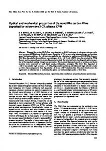
Both the 1.31 eV and 1.68 eV [(Si-V)− ] bands were detected in all samples using PL and optical absorption. A typical absorption spectrum at 77 K is illustrated in Fig. 2(a). The features observed at 1.447 ± 0.001 eV and 1.493 ± 0.002 eV have previously been reported in siliconcontaining diamond.22,35 The intensities of these features were found to correlate with the intensity of the 1.31 eV peak by
(a)
(b)
FIG. 2. (a) NIR absorption and (b) PL spectra of sample A (after annealing at 2000 ◦ C), taken at 77 K. In the absorption spectrum the peaks at 1.447 ± 0.001 eV and 1.493 ± 0.002 eV related to the photoconductivity threshold at 1.5 eV are visible.35 The photoconductivity produces a rise in absorption which partially obscures the vibronic band of the 1.310 ± 0.001 eV feature. Vibronic structure can be resolved in the PL spectrum, though it is noteworthy that the data have not been corrected for the detector response, which decreases with decreasing energy and so may reduce the apparent size of the band. 245208-4
OPTICAL PROPERTIES OF THE NEUTRAL SILICON . . .
PHYSICAL REVIEW B 84, 245208 (2011)
FIG. 3. Raman-normalized PL spectra measured at 5 K of sample A when it was (a) as-grown and (b) annealed at 2000 ◦ C. The 1.31 eV feature was visible in both absorption and PL; all other labeled features were not detected in absorption.
Allers and Collins.35 The result was explained by attributing the peaks to transitions to excited states of the same defect giving rise to the photoconductivity threshold at 1.5 eV.35 The optical transitions that produce the photoconductivity result in a rise in absorption, possibly obscuring the vibronic band of the 1.31 eV ZPL. At 77 K the 1.310 ± 0.001 eV and 1.684 ± 0.001 eV peaks dominated the optical absorption spectra up to the band edge energy. Figure 2(b) shows a PL spectrum recorded with 785-nm excitation at 77 K. The spectrum has not been corrected for the response function of the silicon CCD detector used in this spectrometer. The features at 1.272 ± 0.001 eV, 1.303 ± 0.001 eV, and 1.304 ± 0.001 eV were not observed in absorption. To aid the comparison of different PL spectra,
they have been normalized to the integrated intensity of the diamond Raman peak. In this figure, and those that follow, they are referred to as Raman-normalized PL spectra. Figure 3 shows the Raman-normalized PL spectra (785-nm excitation, 5 K) for sample A, in its as-grown state [Fig. 3(a)] and after annealing at 2000 ◦ C [Fig. 3(b)]. The intensities of the 1.304 eV and 1.31 eV bands do not correlate in different samples and so these features cannot originate from the same defect. The broad emission band centered on ∼1.25 eV appears to correlate with the ZPL at 1.304 eV and is thus associated with its vibronic band. The vibronic coupling in the 1.304 eV system is strong, and overlaps with the vibronic band of the 1.31 eV system, making measurement of this band very difficult. Inspection of the PL spectra shown in Figs. 2(b) and 3(b) reveals that between 77 K and 5 K the intensity of the 1.31 eV ZPL falls significantly and the relative intensity of the 1.303 eV and 1.304 eV peaks changes. To investigate the vibronic coupling of the 1.31 eV system the temperature variation of the integrated intensity of its ZPL was measured in absorption and PL for sample A (after it was annealed at 2000 ◦ C); the resulting data are shown in Fig. 4. The experimental data are shown by points and the lines were calculated as described in Sec. IV A. The defect associated with the 1.31 eV ZPL was unambiguously confirmed to be silicon related by comparing the peak energies in absorption of the 1.31 eV and 1.68 eV bands at 4 K in samples containing 29 Si-isotopic abundances of either 4.7% (sample C) or 90% (samples A and B). Both ZPLs were found to decrease in energy by on average 0.4 ± 0.1 meV when the dominant silicon isotope changed from 28 Si to 29 Si (Fig. 5). B. EPR 0
(Si-V) concentration measurements were made using EPR, where it was noted that for sample A (as-grown) the relative intensities of the resonance lines changed depending on whether the magnetic field, B, was aligned parallel to a crystallographically equivalent direction lying in or out of
(a)
(b)
FIG. 4. (Color online) (a) Integrated absorption coefficient of the 1.31 eV ZPL as a function of the sample temperature. The solid curve is the best fit to the data using Eq. (1). (b) Temperature variation of the 1.31 eV ZPL Raman-normalized PL integrated intensity, measured using 785-nm excitation. The broken curve shows the variation in the absorption and is for comparison only. The solid line is the best fit of the data to Eq. (2). Uncertainties on the integrated absorption and the Raman-normalized PL integrated intensity measurements are estimated to be ±10%. These experiments were made using sample A after it had been annealed at 2000 ◦ C. 245208-5
U. F. S. D’HAENENS-JOHANSSON et al.
PHYSICAL REVIEW B 84, 245208 (2011)
FIG. 5. (Color online) Visible/NIR absorption spectra obtained at 4 K for samples B (thin, blue line) and C (thick, red line), which have 29 Si isotopic abundances of 90% and 4.7%, respectively. The spectral intensities have been normalized to the maximum height of the each band to facilitate comparison. The (a) 1.31 eV and (b) 1.68 eV bands shift to a lower energy by 0.4 ± 0.1 meV when the 29Si abundance was increased.
the {110} growth plane. The EPR spectra acquired for the as-grown sample A with B � �111� are shown in Fig. 6. If the (Si-V)0 centers in a sample were statistically aligned with their �111�-symmetry axes along all crystallographically equivalent directions the resulting spectrum would look like the simulated spectrum [spectrum (c) in Fig. 6]. The spectrum was simulated using the Hamiltonian parameters published by Edmonds et al.21 The integrated absorption of the 1.31 eV ZPL was correlated with the (Si-V)0 concentration in the samples, as measured using EPR. To ensure that charge transfer between (Si-V)0 and (Si-V)− was not induced during the experiments the samples were not exposed to UV light during the EPR measurements. Subsequently, sample handling was carried out in the dark and optical absorption spectra were recorded using monochromatic light, starting at low (