APPLIED PHYSICS LETTERS
VOLUME 84, NUMBER 18
3 MAY 2004
Perpendicular exchange bias in antiferromagnetic-ferromagnetic nanostructures J. Sorta) and B. Dieny SPINTEC (URA 2512 CNRS/CEA), CEA/Grenoble, 17 Av. Martyrs, 38054 Grenoble Cedex 9, France
M. Fraune, C. Koenig, F. Lunnebach, B. Beschoten, and G. Gu¨ntherodt II. Physikalisches Institut, RWTH Aachen, 52056 Aachen, Germany
共Received 21 November 2003; accepted 16 March 2004; published online 20 April 2004兲 Exchange bias effects have been induced along the perpendicular-to-film direction in nanostructures prepared by electron beam lithography, consisting of a ferromagnetic 关Pt/Co兴 multilayer exchange coupled to an antiferromagnet 共FeMn兲. As a general trend, the exchange bias field and the blocking temperature decrease, whereas the coercivity increases, as the size of the nanostructures is reduced. © 2004 American Institute of Physics. 关DOI: 10.1063/1.1737484兴
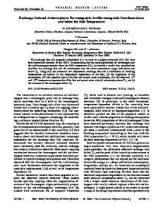
During the last decades, the areal density of data storage devices has dramatically increased each year. This trend demands a miniaturization of the reading/writing magnetic data devices. Reading heads are typically composed of spin-valve or tunnel junction structures, in which antiferromagnetic 共AFM兲/ ferromagnetic 共FM兲 exchange biased bilayers constitute an essential part1 共for recent reviews on exchange bias, see Refs. 2–5兲. It is worth noting that, during the last years, the exchange bias effects arising from reduced dimensions have been investigated to some extent.6 –12 However, so far, these studies have only been carried out in systems with an in-plane magnetic anisotropy. Recently, it has been shown that it is also possible to induce exchange bias in continuous multilayers exhibiting a perpendicular-to-film magnetic anisotropy.13–15 Perpendicular exchange bias offers the possibility of preparing spin valves or tunnel junctions with perpendicular magnetization.16 –18 It should be noted that in order to achieve dense packing of particles 共or nanodevices兲, nanostructures with perpendicular anisotropy are preferable.19–21 In this letter, we demonstrate that it is possible to induce perpendicular exchange bias in nanostructures consisting of a 关Pt/Co兴 multilayer 共ML兲 exchange coupled to FeMn. Our results show that the magnitude of exchange bias decreases as the lateral size of the nanostructure is reduced. Moreover, the temperature at which exchange bias disappears during heating also decreases when the continuous film is patterned. A continuous multilayer with the composition 关 Pt(20 Å)/Co(4 Å) 兴 5 /Pt(5 Å)/FeMn(130 Å)/Pt(20 Å) was deposited onto a thermally oxidized Si wafer by dc magnetron sputtering. From the sputtered multilayer, different types of nanostructures were fabricated by electron beam lithography 共for a recent review on fabrication and properties of magnetic ordered arrays of nanostructures, see Ref. 22兲. Shown in Fig. 1 are the scanning electron microscopy images of 共a兲 the 200⫻200 nm2 square dots, 共b兲 the 200 nm ⫻1 m stripes and 共c兲 the 200 nm⫻100 m wires. The continuous film and the nanostructures were field cooled under a a兲
Author to whom correspondence should be addressed; electronic mail:
[email protected]
field of 2.5 kOe, applied perpendicular to the film plane, from T⫽600 K. Hysteresis loops were measured by polar Kerr effect. Figure 2 shows the hysteresis loops of 共a兲 the continuous film, 共b兲 the 200-nm-wide⫻100- m-long wires, 共c兲 the 200 nm⫻1 m stripes and 共d兲 the 200⫻200 nm2 dots. All the hysteresis loops are rather square, with a remanence to saturation ratio, M R /M S , close to 1. In arrays of very small dots, it is rather common to observe a broad distribution of switching fields.22 This probably accounts for the slight tilt of the hysteresis loop observed in the 200⫻200 nm2 dots. The good squareness of the loops indicates that the perpendicular effective magnetic anisotropy is essentially maintained during the patterning process. Since the perpendicular anisotropy in 关Pt/Co兴 ML arises from the interface anisotropy between the Pt and Co layers,23 it is likely that the Pt/Co interfaces remain parallel to the thin film plane after the patterning. The magnitudes of the coercivity, H C , and the exchange bias field, H E , for the continuous film and the different nanostructures investigated are shown in Table I. It is worth noting that in the 200⫻200 nm2 dots H C increases by a factor of 4 compared to the continuous film. On the contrary, H E decreases from 223 Oe 共in the continuous film兲 to about 14 Oe 共in the smallest dots兲. The enhancement of H C is commonly observed in patterned elements and is probably due to the role of the edges of the nanostuctures as barriers for the domain wall propagation. The decrease of H E as the size of the nanostructure is reduced has also been sometimes observed in AFM-FM patterned elements with in-plane magnetic anisotropy.7,8,10 This decrease can be attributed to the constraints imposed by the reduced dimensions of the nanostructures on the formation of antiferromagnetic domain walls. Indeed, the majority of models dealing with exchange bias relate the magnitude of H E to the formation of domains in the AFM layer.24 –26 It can be argued that the existence of AFM domain walls allows a small surplus of magnetization at the AFM/FM interface, which couples to the FM, resulting in the unidirectional anisotropy, i.e., exchange bias. In fact, taking into account the values of the magnetic stiffness for FeMn (A FeMn⫽3⫻10⫺7 erg/cm) and its magnetic anisotropy (K FeMn⫽1.3⫻105 erg/cm3 ), the domain wall width in
0003-6951/2004/84(18)/3696/3/$22.00 3696 © 2004 American Institute of Physics Downloaded 10 Jan 2005 to 158.109.54.147. Redistribution subject to AIP license or copyright, see http://apl.aip.org/apl/copyright.jsp
Sort et al.
Appl. Phys. Lett., Vol. 84, No. 18, 3 May 2004
3697
FIG. 2. Hysteresis loops measured at room temperature by polar Kerr effect, of 共a兲 the continuous multilayer, 共b兲 the 200-nm-wide nanowires, 共c兲 the 200 nm⫻1 m stripes, and 共d兲 the 200⫻200 nm2 dots.
FIG. 1. Scanning electron microscopy 共SEM兲 images of 共a兲 the 200 ⫻200 nm2 square dots, 共b兲 the 200 nm⫻1 m stripes, and 共c兲 the 200 nm ⫻100 m wires, which consist of a multilayer system with the composition 关 Pt(20 Å)/Co(4 Å) 兴 5 /Pt(5 Å)/FeMn(130 Å)/Pt(20 Å).
FeMn, ␦ FeMn , can be estimated to be ␦ FeMn ⫽ (A FeMn /K FeMn) 1/2⬃50 nm. 24 When the lateral dimensions of the nanostructures become about the same order of magnitude as the AFM domain wall width, it is likely that some AFM domain walls, instead of being able to completely form may be just partially developed inside the nanostructures. These partial AFM domain walls may be less effectively pinned than complete 180° AFM domain walls in continuous AFM-FM films, hence leading to the observed decrease of H E in the nanostructures. It should be noted that our results are opposite to a theoretical study27 which predicted an H E enhancement in AFM/FM nanostructures with relatively large AFM anisotropies and an experimental study28 where an H E enhancement was observed in FM dots on macroscopic AFM. Furthermore, it is well known that FM particles tend to lose their magnetic order when their size becomes very small. A reduction of the Curie temperature in ultrafine FM
particles has been experimentally reported29 and theoretically interpreted.30 In addition, a decrease of the Ne´el temperature has also been observed in ultrathin AFM layers or ultrafine AFM particles.31,32 By analogy, it could be argued that in AFM-FM systems, a reduction in the temperature at which exchange bias disappears during heating 共i.e., the so-called blocking temperature, T B ), may be expected if the continuous bilayer is patterned. Indeed, T B has been found to reduce in AFM-FM continous bilayers with very thin AFM layer thickness or very small AFM crystallites.33,34 The temperature dependence of H E is shown in Fig. 3共a兲. As expected, in both the continuous film and the nanowires, H E decreases during heating due to the loss of magnetic order in the AFM. Nevertheless, H E vanishes in the nanowires at a lower temperature (T B ⫽540 K) than in the continuous films 共where T B ⫽570 K). This can be ascribed to an increasing thermally induced unpinning of antiferromagnetic domain walls as the size of the nanostructure is reduced. Moreover, it is remarkable that the overall shapes of the H E vs T curves in the continuous films and the nanowires are quite different. Namely, although in the continuous films this dependence is roughly linear, in the nanowires H E decreases slowly for T⬍400 K and at a higher rate for larger temperatures. This probably indicates that the distribution of local blocking temperatures in the nanostructures is narrower than in the continuous film. In particular, it can be inferred that, during the patterning, those AFM-FM regions of the continuous films with lower local T B may become, in fact, essentially uncoupled. Figure 3共b兲 shows the dependence of H C on temperature for the continuous film and the nanowires. Similar to H E , TABLE I. Summary of the values of the exchange bias field, H E , and the coercivity, H C , evaluated at room temperature, for the continuous film and the different nanostructures investigated in our study.
Continuous film Nanowires 200 nm⫻100 m Stripes 200 nm⫻2 m Stripes 200 nm⫻1 m Dots 200 nm⫻200 nm
H C (⫾5 Oe)
H E (⫾5 Oe)
252 368 370 409 1042
223 138 54 51 14
Downloaded 10 Jan 2005 to 158.109.54.147. Redistribution subject to AIP license or copyright, see http://apl.aip.org/apl/copyright.jsp
3698
Sort et al.
Appl. Phys. Lett., Vol. 84, No. 18, 3 May 2004
and the coercivity increases as the size of the nanostructure is reduced, probably due to the constraints imposed by the small lateral dimensions of the nanostructures on the formation of AFM domain walls. In addition, the blocking temperature of the AFM-FM system is also found to decrease after the patterning process. These phenomena are certainly important to take into account in the implementation of magnetic sensor nanodevices based on spin valves or tunnel junctions with perpendicular anisotropy. This work was supported by the European Community through NEXBIAS Grant No. HPRN-CT-2002-00296.
1
B. Dieny, V. S. Speriousu, S. S. P. Parkin, B. A. Gurney, D. R. Wilhoit, and D. Mauri, Phys. Rev. B 43, 1297 共1991兲. 2 J. Nogue´s and I. K. Schuller, J. Magn. Magn. Mater. 192, 203 共1999兲. 3 A. E. Berkowitz and K. Takano, J. Magn. Magn. Mater. 200, 552 共1999兲. 4 R. L. Stamps, J. Phys. D 33, R247 共2000兲. 5 M. Kiwi, J. Magn. Magn. Mater. 234, 584 共2001兲. 6 Y. Otani, A. Nemoto, S. G. Kim, K. Fukamichi, O. Kitakami, and Y. Shimada, J. Magn. Magn. Mater. 198, 434 共1999兲. 7 M. Fraune, U. Ru¨diger, G. Gu¨ntherodt, S. Cardoso, and P. Freitas, Appl. Phys. Lett. 77, 3815 共2000兲. 8 J. Yu, A. D. Kent, and S. S. P. Parkin, J. Appl. Phys. 87, 5049 共2000兲. 9 R. E. Dunin-Borkowski, M. R. McCartney, B. Kardynal, M. R. Scheinfein, D. J. Smith, and S. S. P. Parkin, J. Appl. Phys. 90, 2899 共2001兲. 10 Y. Shen, Y. Wu, H. Xie, K. Li, J. Qiu, and Z. Guo, J. Appl. Phys. 91, 8001 共2002兲. 11 FIG. 3. Dependence on temperature of 共a兲 the exchange bias field, H E , and A. Hoffmann, M. Grimsditch, J. E. Pearson, J. Nogue´s, W. A. A. Macedo, 共b兲 the coercivity, H C , for the continuous multilayer film and the patterned and I. K. Schuller, Phys. Rev. B 67, 220406共R兲 共2003兲. 12 200-nm-wide nanowires. K. Liu, J. Nogue´s, C. Leighton, H. Masuda, K. Nishio, I. V. Roshchin, and I. K. Schuller, Appl. Phys. Lett. 81, 4434 共2002兲. 13 S. Maat, K. Takano, S. S. P. Parkin, and E. E. Fullerton, Phys. Rev. Lett. 87, 087202 共2001兲. the coercivity also decreases during heating. Interestingly, 14 Ch. Binek, A. Hochstrat, and W. Kleemann, Phys. Status Solidi A 189, 575 although H C is larger in the nanowires at room temperature, 共2002兲. the values of H C for the continuous film and the nanowires 15 F. Garcia, J. Moritz, F. Ernult, S. Auffret, B. Rodmacq, B. Dieny, J. Cabecome similar for T⬎450 K and even slightly smaller in the marero, Y. Pennec, S. Pizzini, and J. Vogel, IEEE Trans. Magn. 38, 2730 共2002兲. nanostructures at higher temperatures, where exchange bias 16 F. Garcia, F. Fettar, S. Auffret, B. Rodmacq, and B. Dieny, J. Appl. Phys. virtually vanishes. In fact, one finds that the difference 93, 8397 共2003兲. 17 H C (550 K) – H C (300 K) is equal to 200 Oe for the continuF. Garcia, J. Sort, B. Rodmacq, S. Auffret, and B. Dieny, Appl. Phys. Lett. ous film, whereas it is equal to 320 Oe for the nanowires. 83, 3537 共2003兲. 18 N. Nishimura, T. Hirai, A. Koganei, T. Ikeda, and K. Okano, J. Appl. Phys. This is an indication that size effects on AFM/FM coupling 91, 5246 共2002兲. are partially responsible for the large H C observed in the 19 A. Moser, K. Takano, D. T. Margulies, M. Albrecht, Y. Sonobe, Y. Ikeda, nanostructures. In addition, the decrease of H C with temperaS. Sun, and E. E. Fullerton, J. Phys. D 35, R157 共2000兲. 20 K. Y. Guslienko, S. B. Choe, and S. C. Shin, Appl. Phys. Lett. 76, 3609 ture is also associated with the characteristic loss of the per共2000兲. pendicular anisotropy in 关Pt/Co兴 multilayers. From Fig. 3共b兲 21 S. Landis, B. Rodmacq, and B. Dieny, Phys. Rev. B 62, 12271 共2000兲. it seems that the FM anisotropy decreases more rapidly with 22 J. I. Martı´n, J. Nogue´s, K. Liu, J. L. Vincent, and I. K. Schuller, J. Magn. temperature in the nanostructures than in the continuous Magn. Mater. 256, 449 共2003兲. 23 M. T. Johnson, P. J. H. Bloemen, F. J. A. den Broeder, and J. J. de Vries, films. Rep. Prog. Phys. 59, 1409 共1996兲. Finally, although structural changes at the AFM-FM in24 D. Mauri, H. C. Siegmann, P. S. Bagus, and E. Kay, J. Appl. Phys. 62, terface or in the bulk of the AFM due to the ion milling 3047 共1987兲. 25 process have not been found to be significant in AFM-FM A. P. Malozemoff, Phys. Rev. B 35, 3679 共1987兲. 26 P. Milte´nyi, M. Gierlings, J. Keller, B. Beschoten, G. Gu¨ntherodt, U. nanostructures with in-plane anisotropy fabricated by elec7 Nowak, and K. D. Usadel, Phys. Rev. Lett. 84, 4224 共2000兲. tron beam lithography, some structural effects, particularly 27 S. Zhang and Z. Li, Phys. Rev. B 65, 054406 共2001兲. edge defects, should not be completely disregarded as par28 K. Liu, S. M. Baker, M. Touminen, T. P. Russell, and I. K. Schuller, Phys. tially responsible for the reduction observed in H E or T B or Rev. B 63, 060403共R兲 共2001兲. 29 F. Huang, M. T. Kief, G. J. Mankey, and R. F. Willis, Phys. Rev. B 49, the increase of H C . 3962 共1994兲. In conclusion, we demonstrate the possibility of induc30 W. H. Zhong, C. Q. Sun, B. K. Tay, S. Li, H. L. Bai, and E. Y. Jiang, J. ing perpendicular exchange bias in nanostructures composed Phys.: Condens. Matter 14, L399 共2002兲. 31 of a 关Pt/Co兴 multilayer exchange coupled with an antiferroY. J. Tang, D. J. Smith, B. L. Zink, F. Hellman, and A. E. Berkowitz, Phys. Rev. B 67, 054408 共2003兲. magnet 共FeMn兲, fabricated by electron beam lithography. It 32 F. Bødker and S. Mørup, Europhys. Lett. 52, 217 共2000兲. is found that, although the patterned elements preserve the 33 S. Soeya, S. Nakamura, T. Imagawa, and S. Narishige, J. Appl. Phys. 77, perpendicular magnetic anisotropy of the multilayer, the 5838 共1995兲. 34 T. Ambrose and C. L. Chien, J. Appl. Phys. 83, 6822 共1998兲. magnitude of the exchange bias field progressively decreases Downloaded 10 Jan 2005 to 158.109.54.147. Redistribution subject to AIP license or copyright, see http://apl.aip.org/apl/copyright.jsp