to derive the reactive power and rms current circulating through ... R. Famngton and F. C. Lee are with the Virginia Power Electronics Center,. Bradley ...
41 I
IEEE TRANSACTIONS ON POWER ELECTRONICS. VOL 8, N O 4. OCTOBEK 1993
Design Oriented Analysis of Reactive Power in Resonant Converters Richard Farrington, Milan M. JovanoviC, and Fred C. Lee, Fellow, IEEE
Abslruct- The effectiveness of resonant converters can be evaluated on the amount of processed reactive power relative to the output power. A number of resonant converters are analyzed to derive the reactive power and rms current circulating through the transformer. The results of the analysis are used to define design guidelines that minimize the circulating energy in the converters and maximize their efficiencies and power densities. The described analysis and design considerations can be easily extended to other resonant and soft-switching topologies.
n I
n I
I
t
I. INTRODUCTION
G
ENERALLY, higher conversion frequencies bring about
the size reduction of the power transformer and filter components and increase the overall power density. In particular, the size of the transformer is determined by the maximum volt-second product applied to the primary winding and the currents flowing through the primary and secondary windings. The maximum volt-second product determines the maximum flux density and dictates the selection of the primary tums and cross-sectional area of the core. At the same time, the currents in the primary and secondary windings, along with their respective number of tums, determine the window area of the core. By increasing the conversion frequency, the voltsecond product decreases, making it possible to reduce the number of primary tums and/or to select a core with a smaller cross-sectional area. The minimum number of primary turns is practically limited by the required tums ratio for a one-turn secondary. Beyond this, any decrease of volt-second product due to a higher conversion frequency can be achieved by a reduction in the cross-sectional area of the core. However, this trend occurs only in a limited frequency range because the core and copper (winding) losses also increase as the frequency increases, thus reducing the efficiency of the transformer. As a result, operating a transformer above a certain frequency no longer results in a size reduction, but on the contrary, requires a larger core to handle the increased core and copper losses. This frequency strongly depends on the magnetic material. Depending on the application, the frequency range of 200 kHz to 1 MHz seems to be optimal for most high frequency magnetic materials used today. Manuscript received October 26, 1992; revised July 26. 1993. This work was supported in part by the Center for Innovative Technology (CIT) and the Virginia Power Electronics Center (VPEC). R. Famngton and F. C. Lee are with the Virginia Power Electronics Center, Bradley Department of Electrical Engineering, Virginia Polytechnic Institute and State University, Blacksburg, VA 24061. M. M. JovanoviC is with DELTA Power Electronics Lab., Inc., Blacksbug, VA 24060. IEEE Log Number 92 13640.
Fig. I .
Power flow in PWM dc/dc converters.
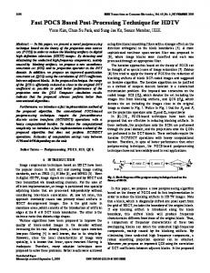
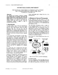
Generally, the transformer current and voltage in isolated PWM converters are square-wave and without a noticeable phase-shift, as represented in Fig. 1. As a result, only real power is processed through the power transformer, and virtually no circulating energy (reactive power) is generated during the power processing. However, as switching frequencies increase into the megahertz range, PWM converters suffer from excessive switching losses. To reduce switching losses and make high frequency operation possible, a number of resonant and soft-switching converters have been proposed [ 11-[ 161. These converters utilize controlled resonances of reactive parasitics and/or extemally added resonant components to achieve zero-current of zero-voltage switching of the power switches and/or rectifiers. Generally, due to continuous resonances, resonant converters have sinusoidal-type currents and/or voltages. In addition, in the majority of resonant converters, the primary current and voltage of the transformer exhibit a significant phase shift that results in a substantial reactive (circulating) power flow as shown in Fig. 2. Although the resonant converters with in-phase primary current and voltage do not circulate power, they still suffer from increased current and voltage stresses compared to their PWM counterparts. In soft-switching converters resonances occur only during short switching transitions so that their currents and voltages are closer to square-type waveforms of PWM converters. To achieve soft-switching for a wide range of operating line and load conditions, resonant-type converters usually need to be designed with a large amount of circulating energy (reactive power) [I]. As a result, the amount of power processed by the transformer in a resonant-type converter is usually significantly greater than that of a similar PWM converter with the same rated output power. Therefore, the size of the power
0885-8993/93$03.00 0 1993 IEEE
IEEE TRANSACTIONS ON POWER ELECTRONICS. VOL. 8, NO. 4, OCTOBER 1993
412
Fig. 2.
Power flow in resonant-type dc/dc converters.
transformer in high-frequency resonant-type converters is not necessarily smaller than the size of the power transformer of the corresponding PWM converter operating at a lower switching frequency. In addition, to process the increased amount of power, resonant converters require switches with higher voltage and/or current ratings. This has a detrimental effect on the overall efficiency of the power stage due to increased conduction losses, especially when a power FET is used. In this paper, a new methodology is presented to measure the effectiveness of power conversion. It is based on the analysis of the reactive power processed by the power transformer as an indicator of the amount of circulating energy in the resonant network. In addition, the current stresses of the power switches are derived for a number of resonant converter topologies. The results of the analysis are used to define design guidelines that minimize circulating energy. The analyzed converter topologies include the half-bridge zero-currentswitching quasi-resonant-converter (HB ZCS-QRC) [ 11, the half-bridge zero-voltage-switched multiresonant-converter (HB ZVS-MRC) [5], the constant frequency half-bridge zerovoltage-swiched multiresonant-converter (CF HB ZVS-MRC) [6], [16], the HB ZVS that uses the magnetizing inductance as a resonant element (HB ZVS-MRC ( L b f ) )[7], [16], and the full-bridge series-parallel-resonant-converter (FB SPRC) [8], [ 131, [ 161. Although only bridge-type topologies are presented, the analysis and conclusions can be easily extended to any other topology.
the switching devices (MOSFET's and rectifiers). Equivalent circuits for each topological stage are solved analytically, assuming that the capacitor voltages and inductor currents are continuous at the boundaries of two consecutive topological stages. However, due to the nonlinear nature of these converters and the larger number of modes of operations (sequences of topological stages) usually encountered in resonant-type converters, a numerical algorithm is necessary to obtain the desired waveforms. Recently, this approach has been successfully used to obtain the dc characteristics of a number of quasiand multiresonant converters [ I], [5]-[7], [ 121, [13], [ 161. In this paper, the described approach is extended to calculate the real, reactive and apparent power flowing through the power transformer and current stresses of the switches of the discussed converters. Since the currents and voltages of the analyzed converters are not true sinusoids, the contributions of higher voltage and current harmonics to PI^. and &I\, have to be taken into account. By applying a Fourier decomposition to the primary voltage and current waveforms, the accurate calculation of real, reactive, and apparent power PA. processed by the transformer can be obtained. The Fourier representation of the primary transformer voltage and current is given by
n
IPRISl(t)
=
I ~ R I sin(nwot ~ I ~ ~
+ 4n)
(2)
0
where V ~ R I Iand \ . ~I~~ ~ R Irepresent RI~~ the nth harmonic of the primary transformer voltage and current respectively, and & is the phase shift between the primary transformer voltage and current waveforms. From the Fourier representation of these signals the real power, reactive power, and apparent power can be obtained from the following expressions:
(4) where = (C;V&Ih1n/2)1/2 and I;'& = (E~1&1h1n/2)1/2are the primary rms voltage, and current and PLVand P.4 are the real and apparent power, respectively. Thus, the reactive power processed by the transformer is
11. ANALYSIS OF REALAND REACTIVEPOWER
Due to the process of reactive components, the power processed by the power transformer of a resonant converter consists of real ( P w ) and reactive (Qm,) power. To calculate Pu. and Q w , it is necessary to determine the primary voltage and primary current waveforms. For the five converters considered in this paper, the primary voltage and current waveforms are determined analytically using the approach described in [4]-[7], [ 121, [16]. In this approach, the operation of a converter during a single conversion cycle is divided into several topologies stages corresponding to different states of
Finally, the effectiveness of the transformer in transferring power can be defined as the ratio of the apparent power and real power, i.e.,
For the best transformer utilization and, consequently, minimum transformer size, y should be equal to one. In this case, the transformer processes only real power, since it operates with unity power factor (pf = 1).
FARRINGTON
el
al.: ANALYSIS OF REACTIVE POWER
413
IN
A
IN
P
+
R L vo
IN
CD
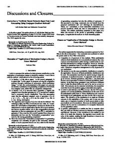
(c) Fig. 3 .
Circuit diagrams and primary transformer voltage and current waveforms for different resonant converters. (a) HB ZCS-QRC. (b) HB ZVS-MRC ( L . ~ J (c) ) . HB ZVS-MRC.
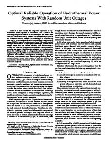
Figs. 4-8 show the dc conversion ratio M , the power transfer effectiveness of the transformer y,and the normalized primary current (I;’&) characteristics for the five converters (Fig. 3). It should be noted that the SPRC characteristics in Fig. 8 were obtained by taking into account the primary switch capacitance [12]. The characteristics are all plotted as a function of fcon/fo(z-axis) for different normalized load (7) currents I,, with the exception of the characteristics of the SPRC which are given for different values of the normalized The relationship between peak switch current IC: and I;.’;tSsr load resistance Q. For every operating point on the dc characdepends on the shape of the primary current waveform. teristics ( M ,f c o n / f o . Ion), the ratio of the apparent power to is However, the upper boundary of I:$ the real power processed by the transformer can be determined rms( max) (8) by reading the y value for the corresponding fcon/fo. The I hIPRIM normalized rms primary current can be determined in a similar where the equal sign is used for distortion-free sinusoidal manner. For example, the dc operating point defined in a waveforms. For converters with quasi-sinusoidal waveforms, gain characteristic can be mapped into the and I ; such as those Of Fig. 3(a)3 3(c), 3(d)3 and 3(e), the peak characteristics, as shown in Fig. 4. Conversely, any point in switch CUrrent 1s Close to the limit given in (8). On the the or /;;m~s%~characteristics can be mapped into the two other hand, for Converters with Predominantly squae-wave remaining characteristics. The relationship between the real shape of the primary current, such as in the converter of Fig. and reactive power as a function of 7 is 3(b), the peak switch current is closer to the rms primary
The Fourier decomposition is also used to calculate the This current true rms value of the primary current (/?&). not only determines the copper loss in the primary winding, but also determines the current stresses and losses of the primary switches. Generally, for half-bridge and full-bridge type converters, the rms current of the primary switch is
current, i.e., $ :/
= I;.’;;?~~.
=
tan(cos-’(l/Y)).
(9)
~
~
~
414
IEEE TRANSACTIONS ON POWER ELECTRONICS, VOL. 8, NO. 4, OCTOBER 1993
+ VO
V IN
+
V IN
VO
lPRM -IdN
4 ______
(e)
Fig. 3 . Circuit diagrams and primary transformer voltage and current waveforms for different resonant converters continue. (d) CF HB ZVS-MRC. ( e ) IT3 SPRC.
111. DISCUSSION As can be seen from Figs. 4-8 the HB ZCS-QRC and the HB (close , to ZVS-MRC ( L M )have relatively small y = P A / P ~ unity). As a result, these two converters circulate very small amounts of power between the primary and the secondary circuits. The HB ZCS-QRC has the best overall power-transfer effectiveness among the analyzed converters. As seen from Fig. 4 the worst case power transfer effectiveness, which occurs at full load, is y = 1.18, and is independent of frequency. In this converter, power is transferred from the primary to the secondary only during the on-time period of switching cycle. Most of the power processed by the transformer is delivered to the load because the primary current and primary transformer voltage are in phase (Fig. 3(a)).
The presence of small amounts of reactive power (y # 1) results mainly from harmonic distortion of the primary voltage waveform. Due to the resonance of the switch current that is used to create conditions for lossless tum-off, the rms primary current in the HB ZCS-QRC is higher than that in the PWM HB circuit, as shown in Fig. 4(c). Thus, the conduction losses in the transformer and the semiconductor switches are increased compared to the HB PWM Besides the HB ZCS-QRC, the HB ZVS-MRC ( L M )does not suffer from excessive circulating power during heavy load operation. As can be seen from Fig. 5 , for conversion frequencies below 1.5 of the resonant frequency, y is independent of load. In addition, for dc voltage-conversion-ratios close to one and for f c o ~ / f o< 1 . 3 , ~5 1.2. Therefore, a
FARRINGTON
er
415
al.: ANALYSIS OF REACTIVE POWER
1
0.8
' 0.8
M= X
O
.
v,
,
YN /2N
ai
VIN/~N 0.4
0.4
0.2
0.2
fC+/fO
8
Y
6
Y 4
2 1
1.2
'.4
fcor no
1.6
(b) 1.4
1.2
1
0.8 0
0.2
0.4
0.6
0.8
1
fconflo 0.6
Fig. 4. HB ZCS-QRC. (a) DC voltage conversion ratio. (b) Transformer power transfer effectiveness. (c) Normalized primary rms current. ~S= . and Characteristics are for Ioy = 2 l o Z ~ ~ / l iZo fo = 1/-. where L is the leakage inductance of transformer.
Jm.
properly designed converter, which at heavy loads operates with f c o N / f o < 1.3, does not circulate a significant amount of power. The good power transfer effectiveness is due to a very short resonant interval in comparison to the switching period, and the absence of any resonance between reactive elements on different sides of the transformer. That is, the energy stored in the magnetizing inductance at the beginning of every switching transition is used to operate the active switches under ZVS, while the linear inductors located on the secondary side are used for charging and discharging the capacitance in
1
1.2
1.4
1.6
fconflo (C) Fig. 5. HB ZVS-MRC ( L n l ) . (a) DC voltage conversion ratio. (b) Transformer power transfer effectiveness. (c) Normalized primary rms current. Characteristics are for C.y = 10, and L.y = 3. where Clv = ~ C D / C ~ V ~ . L=! V 4 L . h l / L N 2 and IOU = ~ ~ o Z O / L ~ N = Y.Z~ and fo = 1 / d G - .I s m is the current through the linear inductor when the corresponding saturable inductor saturates.
d m .
parallel with the rectifier diodes in a controlled fashion. In addition, this converter has square-type primary current and switch current waveforms [ 7 ] , [16], so that their rms values are only slightly higher than those in the PWM HB circuit,
IEEE TRANSACTIONS ON POWER ELECTRONICS, VOL. 8, NO. 4, OCTOBER 1993
416
1.7
1.6
Y 1.5
1.4
1.6
1.4
'-
1.2
IltlS
PRIM
'om
1
0.8
0.6 0.5
1
1.5
0.5
fcon/fo
1
fconlfo
1.5
(b)
(a)
Fig. 6 . HB ZVS-MRC dc voltage conversionratio, transformerpower transfer effectiveness, and normalizedprimary rms currentcharacteristics. (a)C, = 10. where CN = ~ C D / C N ~ , I O = N2loZo/&",Zo = and fo = 1 / a . Operating point A corresponds to low-line and full-load conditions. @)CN = 5 where CN = ~ C D / C N ~ =, I2 1~0 ~Z o / ~ N N , Z o = and fo = l/m. Operating point A corresponds to low-he and full-load conditions.
m,
Fig. 5(c). As a result, the soft switching of the semiconductor components is achieved without significantly increasing their conduction losses. The added components on the secondary side ( S L ,L , and C D )have a minimal effect on the efficiency and the size of the converter, since the saturable reactor S L and linear inductor L can be integrated on a single core [7]. The HB ZVS-MRC (Fig. 6), the CF HB ZVS-MRC (Fig. 7), and the FB SPRC (Fig. 8) circulate relatively large amounts of power. For these converters, the circulating power is a strong function of the load ( I O N and ) line ( M )conditions, as well as of the values of the reactive components. For example, in the
m,
multiresonant converter [Fig. 3(c)], a higher ratio of rectifier capacitance CD to the switch capacitance C, i.e., CW = Z C D / ( N ~ Cresults ), in increased circulating power when dc operating points with the same IONand A4 are compared. This effect is more noticeable at lighter loads (i.e., ION = 2 , 1 , . . .)l as can be seen by comparing y in Fig. 6(a) and (b). Similarly, a higher ratio of the series to parallel capacitances Cs/Cp in the SPRC results in smaller circulating power as can be seen by comparing y in Fig. 8(a), (b), and (c). For these two converters, dc operating conditions with minimum circulating energy (minimum y) occurs for heavy loads (ION= 5,10, . . . , in Fig. 6, and Q = 0.25,0.5,. . . in Fig. 8). Even when
417
FARRINGTON er al.: ANALYSIS OF REACTIVE POWER 25
2
0.5
0.8
1.4
A 4.5
4
3.5
Y
3 2.5
Y
2 1.5
0.8
1
1.2
fcontfo
1.4
4
3.5
14
3
12
2.5
10
2
I= lo/N
1.5
6 1.1
fconlfo
4
(a)
2
Fig. 7. CF HB ZVS-MRC. (a) DC voltage conversion ratio. (b) Transformer power transfer effectiveness. (c) Normalized primary rms current. Characteristics are for C,v = 10. and f r O N / f c l = 0.250.6 is defined as the normalized time duration (with respect to 1/ fo)between the tum off time of the secondary side switches (constant-frequency switches) and the primary switches, and fo = l/-,Zo = and Iox = ' 2 l ~ Z o / l i x . T .
m.
a dc operating point with minimum circulating energy is selected, the apparent power processed in the transformer of the HB ZVS-MRC and SPRC is approximately 1.4 times the real (output) power. This corresponds to circulating power comparable to the output power, since for PI%= QI~ = 3 ?
Fig. 8. (a) FB SPRC dc voltage conversion ratio, transformer power transfer effectiveness, and normalized primary rms current characteristics for C,b/C = 10 and C , s / C p = 2 . Operating point .A corresponds to low-line and full-load condition. Q = R/Zo.lo~ = IoZo/liri-T.Zo = m . f o = 1/-> and C,,, = C,\Cp/(C\ Cr).
+
+
PA4/Ptt~= J1 ( & ~ - / P t v=) ~A. Therefore, the power transformer for the best possible design in the ZVS-MRC and SPRC handles roughly twice the power of the transformer in the corresponding PWM circuit. In addition, the converters with increased circulating power (i.e., ZVS-MRC, CF ZVSMRC, and SPRC) also suffer from increased primary rms currents. The rms primary current shows the same trend with respect to load and line conditions as does y. As a result, to
I EEE TRANSACTIONS ON POWER ELECTRONICS, VOL. 8. NO. 4, OCTOBER 1993
418
2.5
vo
YN/N
2
vo YN I N
1.5
1
0.5
0.0
1
1.1
1.2
1.3
1.4
1.5
0.0
fconno
1
1.1
1.2
1.3
1.4
‘
1.3
1.4
1
I
fconRo
8 8
7
5
6
4
Y
Y
5 4
3
3 2 2
1.5
1.5
fcon/fo
0.9
1
1.1
1.2
fcon/fo
5
4
____~_____~____
&$I Io/N
3
2
1.25
09
1
fcon/fo
1 1
12
fcon/fo
13
14
15
(h)
(c 1
Fig. 8. (Cont.’d) (h) FB SPRC dc voltage conversion ratio, transformer power transfer effectiveness, and normalized primary rms current characteristics for C , / C = 10 and C\/Cp = 1. Operating point .I corresponds to low-line and full-load condition. Q = R/Zo.Iox = Ic>Zo/\ix.\-. 20 = fc? = l / G . and C,,, = C S C P / ( C \ C p ) .
Fig 8 (Cont.’d) (c) FB SPRC dc voltage conversion ratio, transformer power transfer effectiveness, and normalized primary rms current character:stics for C \ / C = 10 and C\/Cp = 0 5 Operating point 4 corresponds to low-line and full-load condition c? = R/Zo.IoN = Iozo/\ih-y.zo = m , f o = I/@?&? and = C\CP/(C~ Cp)
accommodate larger power and rms currents, the size of the transformer in these converters has to be larger than the size of the transformer in the corresponding PWM converter operating at a similar frequency. In addition, these converters require primary switches with higher current ratings to handle the increased rms currents. Table 1 shows typical utilization factors of the primary switches for all of the analyzed converters operating with minimum circulating energy. The transistor
utilization factor is defined as the ratio of the output power divided by the number of switches to the product of the peak voltage and current seen by these switches. The largest amount of circulating power and its strongest dependence on load and line conditions are found it the CF HB ZVS-MRC, Fig. 7(c). In applications with wide inputvoltage and/or load range, this converter exhibits very poor efficiency at medium and light loads. As a result, its potential
+
m.
ce,,
+
419
FARRINGTON et al.: ANALYSIS OF REACTIVE POWER
SWICH UTILIZATION
I
TABLE I FACTORSFOR ANALYZED B R I ~ GCONVERTERS E
Topology
PWM ZCS-QRC ZVS-MRC (LM) ZVS-MRC CF ZVS-MRC SPRC
I
Switch U.F.
I
0.25 II 0.10 U 0.21 N 0.15 N 0.12 N 0.15 -N
applications are limited to those with narrow input-voltage and load variations, such as the ones encountered in the systems with power-factor corrector.
I v . DESIGNOPTIMIZATION BASEON MINIMIZATION OF REACTIVEPOWER Since the HB ZCS-QRC and the HB ZVS MRC ( L ~ I do not circulate significant amounts of power, their design optimization procedures are relatively simple and are based on criteria other than the minimization of the reactive power as described in detail in [7], [ 1I], [ 161. On the other hand, for the HB ZVS-MRC, CF HB ZVS-MRC, and the SPRC, design optimization guidelines that maximize their overall efficiencies can be defined based on the minimization of the reactive power. As discussed in the previous section, the rms primary current (as well as the secondary currents) exhibits the same trend as the reactive power, i.e., regions of operation with smaller reactive power also have smaller rms primary currents. Consequently, the minimization of the reactive power results in the minimization of the conduction losses, and therefore maximizes the overall efficiency. Due to the limited number of applications in which the CF ZVS-MRC can be used, design examples for this converter are not considered in this paper. In this section, several design examples for the HB ZVSMRC and SPRC, which use the characteristics presented in Figs. 6, 8, and 9 to identify the regions of operation with minimum circulating energy are presented. The boundaries of the region of operation are determined from the line and load specifications. For example, point A in Fig. 6(b) represents low-line ( Yiin), full-load ( I r a " ) operating point, while point B corresponds to the high-line (k;;"") full-load ( I F " ) operating point. Similarly, points C and D in Fig. 6(b) light-load (IF'") and lowcorrespond to the high-line ( yzax), , light load (If'") operating points, respectively. line Low-line operating points A and D lie on the M""' = V,/(V,gin/2N) line, while high-line (V,;"") operating points B and C lie on Mmin = V"/'c;Ea"/2N) line. These four points completely define the operating region for the given design specifications. For example, the HB ZVS-MRC can be designed to operate in the region shown in Fig. 6(a). From the y characteristics [Fig. 6(b)], it can be seen that this design (design #1) does not minimize the circulating power. The amount of circulating power can be minimized by selecting the operating regions, as
(Yi'")
shown in Fig. 9(a). Regions of minimum circulating energy are selected by specifying the low-line full-load operating points (point A ) at minimum y on the selected ION curves. Design #2 and design #3 circulate the same amounts of power under full-load and low-line conditions (y M 1.4) which is less than in design #1 (y x 1.45). However, design #3 requires a transformer with a substantially lower tum ratio than design #2 (0.45/0.87 M 0.5). Therefore, design #2 has lower conduction losses on the primary side and maximum overall efficiency under heavy load conditions. In addition, design #2 will operate with a narrower switching frequency range. It should be noted that by selecting the full-load, lowline operating point on a curve with ION 2 (point A in design #4 in Fig. 9(a)), the tums ration of the transformer can be slightly increased in comparison with design #2. However, the circulating power in this design would be larger since y increases dramatically at lower values of ION. A higher transformer tums ratio for the same Igr can be obtained by selecting a characteristic with higher C N , for example design #5 in Fig. 9(b). This design clearly results )in higher reactive power compared to design #2. To compare conduction losses (I;'&) of design #5 relative to design #2, it is necessary to determine the relative tums ratio of the transformers since the rms primary current is given in the normalized form. The tums ratio of the transformer in design #5 has a larger number of tums because the low-line, full-load operating point (point A in Fig. 9(a)) is selected at a higher dc gain (M#mgaxM 1) compared to design #2 (M#","" M 0.8). In fact, the number of tums of the transformer N (= #), in design #5 is N#5 = MFy/M$y M 1.25N#2 Therefore, the maximum rms primary current for design #5 (operating point A ) is = 1.2I,"""/1.2N#2 = 0 . 9 6 I r / N # 2 M I;'&#c1 i.e., approximately equal to the rms primary current for design #2. Since design #2 circulates less power it is more efficient than design #5. From the y characteristics of the SPRC shown in Fig. 6 for different ratios of series to parallel capacitances C s / C p , it can be seen that the circulating power is a strong function of Cs/Cp for high values of Q, i.e., Q > 0.75. The circulating power decreases as the ratio of these capacitances increases. For example, for Q = 1 and in the vicinity of the resonant frequency f c O N / f o = 0.9-1.0, y is approximately 4 for C s / C p = 0.5 [Fig. 8(a)], approximately 3 for C s / C p = 1 [Fig. 8(b)], and 2.5 for C s / C p = 2 (Fig. 8(c)). However, for lower values of Q (i.e., Q < 0.75), the amount of circulating power is almost independent for Cs/Cp. For Q = 0.25, for example, y is in the range of 1.5 to 1.75, regardless of the C s / C p ratio. The rms primary current shows a similar trend as the circulating power with respect to the C s / C p ratio. Generally, higher values of Cs/Cp result in smaller rms primary currents. This trend continues for lower Q values. For example, normalized rms primary currents for Q = 0.25 and around the resonant frequency are approximately 1.75, 1.3, and 1.1 for C s / C p = 0 . 5 , l and 2, respectively. To minimize the circulating power in the SPRC, it is necessary that the lowline full-load operating point (point A on the dc characteristics in Fig. 8) be placed at the maximum gain ( M = V , / V N / N