Unlike conventional SDRAM, Rambus uses a relatively narrow bus clocked at a high speed to achieve an equivalent bandwidth. Rambus includes various other.
Reconfigurable Memory for Reconfigurable Computing Philip Machanick, Peter Sutton and Adam Postula School of ITEE, The University of Queensland, St Lucia Qld 4072 Australia {philip, p.sutton, adam}@itee.uq.edu.au
Abstract Significant problems have inhibited the wide adoption of reconfigurable computing, including the difficulty of programming them, and the difficulty of interfacing processor cores to external devices and memory. This paper proposes a strategy for dealing with the external interface problem, starting from a reconfigurable memory system design. The memory system design is based on I/O principles and could therefore become the basis for an I/O interconnect. Keywords: reconfigurable computing, FPGAs, memory hierarchy, input-output
1. Introduction Reconfigurable computers based on FPGAs have shown great promise in accelerating many applications beyond supercomputer speeds at a fraction of the cost. By exploiting parallelism, reconfigurable computers (also called configurable computers or custom computers) have demonstrated superior performance for applications in the areas of long integer arithmetic, cryptography, error correction, image analysis, stereo vision, video compression, sound synthesis, neural networks, high-energy physics, thermodynamics, biology and astronomy [5][16]. In some cases the cost is 100 times less ($ per operation per second) than using a supercomputer [16]. Reconfigurable computers, however, have not yet met with commercial success. The main reason for this is application specificity. Most reconfigurable computers have an I/O and memory architecture specialised for accelerating a particular algorithm. The architecture is usually sub-optimal for other similar highly-parallelisable tasks and down-right inefficient for significantly different algorithms.
1
Reconfigurable computing remains an area of great potential. The performance per cost advantage of reconfigurable computers for many algorithms is unlikely to be diminished. Even though microprocessor performance is advancing rapidly over time, the same can be said for FPGA performance. Both are implemented with leadingedge fabrication processes and exhibit similar “Moore’s law” trends in capacity and clock-speed. Memory, however, is another issue. Since the mid1980s, while processor speed has been improving by 50100% per year, DRAM latency has only been improving by 7% per year [9]. As FPGA capabilities improve, reconfigurable computer performance will increasingly be limited by memory speed – a problem which has already been a concern for some years with conventional computers [11][20]. If a reconfigurable computer is to be competitive in performance with a supercomputer, it needs to have a memory subsystem capable of meeting similar requirements to that of a supercomputer. Given that the processor can be reconfigured, the memory system also needs to be reconfigurable to support different algorithm styles. The design proposed here aims to make reconfigurable computing architectures more general, by providing a flexible, reconfigurable memory. While a reconfigurable computer with the proposed memory system would still not be general-purpose, it should be able to compute a wide-variety of highly-parallelisable algorithms efficiently. The remainder of this paper is structured as follows. Section 2 motivates the approach. Section 3 outlines design principles for a reconfigurable memory, while Section 4 provides some detail of how those principles could be put in practice. Section 5 concludes the paper with a summary of the key ideas, and a proposal for future work.
2. Background
2.1.2 Solutions
This section provides some background of the general problem of DRAM performance and high-performance solutions which have historically been adopted, as well as some background of the reconfigurable computer area.
The most obvious solution to the latency problem is to access more than one column after the RAS cycle, to amortize the investment in setting up a row for access. Many variations on this idea have been designed. The most recent are variations on synchronous DRAM (SDRAM), in which the DRAM cycle time is synchronized to the memory bus for improved performance but, more significantly, a DRAM access combines multiple column accesses with one row access [7]. Another variation is Rambus, which, like SDRAM, can set up multiple column accesses after an initial row access. In common with recent variations on SDRAM, Rambus transfers data on both the rising and the falling clock edge. Unlike conventional SDRAM, Rambus uses a relatively narrow bus clocked at a high speed to achieve an equivalent bandwidth. Rambus includes various other enhancements, including an internal organization with the effect of multiple banks of DRAM [6]. Rambus has some drawbacks. Adding complexity to each chip exacts a price premium, which has made it unpopular in the mass market. Further, its organization increases latency as more DRAM chips are added because the bus is in effect lengthened. HyperTransport has some features in common with Rambus. It is also based on a relatively narrow bus clocked at a high speed, and has design features aimed at reducing complexity of board-level design [1]. However, HyperTransport is not specific to a given DRAM design – it is a general-purpose interconnect –!and therefore offers opportunities for more general design. Multiple memory banks are a common design feature in traditional high-end supercomputers, and the specific layout of memory has been shown to be a significant issue in achieving high performance [14]. A multibanked DRAM has memory modules organized to be separately addressable, so the latency of a specific RAS-CAS cycle can be overlapped with a previous transfer. Provided there are different sources of memory references, a multibanked memory system can both hide latency and achieve high bandwidth. A further refinement is to provide an interconnection network designed to minimize conflicts between requirements of multiple processors, as opposed to a simple single bus between memory and the processing module [15]. In systems with multiple memory banks, it is also important for applications to distribute data in memory in such a way that contention is minimised when multiple processors access multiple memory banks. Such a data placement problem will also apply to the reconfigurable memory system proposed here. However, it becomes simpler when the memory subsystem can be reconfigured to suit the algorithm. Some theoretical foundations for optimisation of data placement and memory interconnect for interleaved memory systems are available in [3].
2.1 DRAM Issues In general terms, the latency trend for DRAM is leading to a situation where performance improvement requires close attention to memory organization. Consequently, performance differentiation between classes of computer is increasingly becoming a property of DRAM and peripheral organization, rather than of CPU design. If this trend persists, design features of highend supercomputers of the past, which had aggressive DRAM and peripheral subsystems, may become more mainstream. This section examines problems with DRAM in a bit more detail, and outlines some solutions, concluding with some which, in the past, have been the province of highend supercomputers. 2.1.1 Problems There are two major performance bottlenecks in DRAM use: latency and bandwidth. The latency problems arise from the access cycle of DRAM. A relatively slow row access strobe (RAS) addresses a row in a 2-dimensional DRAM array. Once a row is selected, a relatively fast column access strobe (CAS) cycle extracts a specific bit from the row. In addition, DRAM also needs periodic refresh cycles. DRAM, then, is relatively slow if a completely random access is required, because the entire row and column addressing cycle is required (potentially compounded by waiting for a refresh cycle). The bandwidth problem arises out of a combination of factors. DRAM, for cost reasons, is typically packaged with a narrow word-width, with only a few bits available on each cycle (historically, only 1, though wider DRAMs are now common). Further, since DRAM is meant to be high-capacity storage of variable size (allowing different cost-benefit trade-offs), it must necessarily be implemented off the processor chip, incurring off-chip delays (another latency cost but also a limit on bandwidth). Finally, conflicting demands on the DRAM system cause design problems in trading latency with bandwidth. If a high-performance peripheral (e.g., a fast disk subsystem) performs best when streaming a large amount of data directly to or from DRAM, other parts of the system (e.g., the processor) could suffer a latency problem by being forced to wait a long time for this large streaming event.
2
2.2 Reconfigurable Computing Issues
which was of sufficient interest to justify the expense of a custom memory system design. The OneChip-98 design, for example, incorporates a fixed memory interface into a reconfigurable logic design, which reduces the memory bottleneck experienced in other reconfigurable computer designs [10], but does not address the need for a reconfigurable memory design. It has been demonstrated that flexibility can be obtained at the cost of performance, on an on-chip memory system [19], but this work has not been extended to off-chip memories. One answer to the objection that reconfigurable computers are hard to program is that the time taken is roughly equivalent to that for highly tuning a similar algorithm on a supercomputer [16]. Work on operating systems for reconfigurable-computing [17][18] will also improve programmability in the future (probably at the cost of performance).
Reconfigurable computing is a promising area, given that exploitation of parallelism on an FPGA leads to the potential of high speedups over a standard singleprocessor algorithm. While there is a growing trend towards supporting increasingly aggressive instruction-level parallelism on conventional processors, an FPGA offers the option of designing custom hardware to support application-specific parallelism. However, there are obstacles to the wide deployment of reconfigurable computing, including the difficulty of programming them, and the difficulty of interfacing them to the outside world. The remainder of this section provides some background on reconfigurable computing, starting with more details of the problems identified here, followed by some solutions, leading to the problem we plan to address. 2.2.1 Reconfigurable Computing Problems
2.2.3 Problem Addressed in this Work Programmability of reconfigurable computers will not be specifically addressed in this work – only the interconnect problem is considered, with specific focus on requirements for memory. The intent, however, is that our design should be sufficiently general to support future work on I/O.
There are several obstacles to wider deployment of reconfigurable computing, including the difficulty of developing specific solutions because of software limitations, and the difficulty of designing custom interconnects for multiprocessor configurations, and for memory and I/O. These problems result in difficult translation from an algorithm to an implementation, and disappointing overall system performance (sometimes no better than a conventional computer), despite the algorithm core on an FPGA being thousands of times faster than a software implementation [2]. Reconfigurable computing presents particular challenges in that different algorithms implemented in programmable logic may have different memory access requirements. For example, an implementation of an FPGAbased special-purpose computer to simulate sintering (an example of using Monte Carlo simulations of physical systems) has used a multibanked memory [13]. In general, a memory bank organization which suits one class of algorithm may not suit another. The ideal case would be to reimplement the organization from scratch for each algorithm with a significantly different pattern of memory usage. A reconfigurable memory subsystem provides this opportunity without having to build a new system. Reconfigurable computers can also be difficult to program, because a great deal more hardware knowledge is required to implement a highly optimised algorithm on a reconfigurable computer than is the case for a conventional computer.
3. Design Principles Our starting point is the fact that DRAM access is increasingly becoming similar to I/O in that the time for setting up a DRAM operation is a significant bottleneck – even if subsequent transfers can happen at high speed. A significant aspect of the design is a reconfigurable interconnect, which will support a range of different topologies for connecting RAM and processor modules. The approach proposed here aims to make reconfigurable computing architectures more generally applicable. It is our hypothesis that a reconfigurable computer with a reconfigurable memory interconnect, designed on principles of a high-end I/O subsystem, will be applicable to a wider variety of highly-parallelisable algorithms than any existing custom design, without significant performance degradation, as compared with a custom design for a specific algorithm. A consequence of proving this hypothesis in our future work will be to provide a basis for a design not only of a reconfigurable memory system, but also an I/O system, though evaluation of the design as an I/O system is reserved for follow-on projects. The remainder of this section examines some ideas which form the basis for our design principles, followed by the strategy we are adopted to put the principles into practice. The section ends with a summary of the key ideas.
2.2.2 Existing Reconfigurable Computing Solutions Existing designs have either had suboptimal memory subsystems, or have been designed for a specific problem,
3
3.1 Basis for Design
The memory interconnect design we advocate should accommodate a range of alternative interconnect strategies for DRAM, allowing the reorganization of the topology when the reconfigurable computer is reprogrammed. We plan to evaluate the approach by comparing its performance against a simulation of a hard-wired multi-module memory scheme, with a topology idealised to each computation.
Trends in available circuitry on a single FPGA device suggest that requirements for fast random-access memory will increasingly be met on-chip. Accordingly, a memory hierarchy in which a large but not necessarily low latency memory can complement fast on-chip memory is looking increasingly useful. Given the growing amount of logic on a single device, the emphasis in external (off-chip) interconnect design is increasingly switching from highspeed interconnection at the logic level to interfacing to large memories or the outside world. As compared with a conventional computer system, we envisage a similar kind of memory hierarchy, with fastest components near the processor and larger, slower components further from the processor. The slower components will take longer to set up a memory operation (higher latency), but should be able to transfer data quickly (high bandwidth), to take maximum advantage of device characteristics (DRAM takes time to set up but can transfer quickly once it has started). The difference from commodity computers is that, as with supercomputers, a range of different styles of memory access needs to be supported. The flexible interconnect has to allow for variations in how demand for bandwidth arises from the style of computation. In some cases, memory may be required in a single stream or burst at a given time, at a given transfer rate. In other cases, given the highly parallel nature of programmable logic devices, multiple streams may be required.
3.3 Summary Our approach is one of seeing large-scale memory requirements increasingly taking the form of I/O in the sense that bandwidth goals are likely to be easier to achieve than bandwidth goals. Nonetheless, it is useful to base our key ideas on an I/O architecture which was designed to minimize latency.
4. Application of the Principles In this section, the ideas previously described are fleshed out. The general principle of organizing a reconfigurable memory system seems obviously useful, but the details of how to design it require some work. For example, issues which require clarification include the kind of reconfiguration supported, the extent to which trading latency for bandwidth is reasonable and whether reconfiguration should be static (changed only as the FPGA component is reprogrammed) or dynamic (changed during a computation). With a statically reconfigurable interconnect, we envisage that there would be a limited number of alternative routes which could be selected dynamically, whereas a dynamically reconfigurable interconnect would be able to set up routes on the fly. Once the design principles are clarified, it is useful to consider what technologies could fit the goal of using offthe-shelf technologies and designs as far as possible. Finally, some examples are useful to consider as a basis for making the principles concrete. The remainder of this section examines these issues in turn.
3.2 Strategy The approach advocated here is to borrow architectural ideas from high-end I/O designs, such as the IBM 3990 storage subsystem. The 3990 subsystem was designed to minimize latency, while supporting a wide variety and quantity of devices, with a high aggregate bandwidth. This design has survived across decades of improvement in device speed and interconnect technology [8]. One lesson which can be learnt from experience with the 3990 is that providing a variety of alternative paths and devices will in many cases beat having a single higher-speed device with a single higher-speed path, if contention is a factor [12]. It is an interesting question how similar memory and I/O access can be in reconfigurable computing. Our view is that the same or very similar interconnect fabric can be used for both. The utility of this approach is that similar designs and components can be reused for different parts of the system, potentially saving both cost and design time. It is also an important goal to use off-the-shelf technology as far as possible, if this can be done without significantly compromising performance, thereby maintaining the cost advantage of reconfigurable computing.
4.1 Kind of Reconfiguration Given the flexibility inherent in reconfigurable computing, the question arises of a reconfigurable memory system: “How reconfigurable?” Some algorithms, for example, may require efficient bit-level addressing. Others may work with vectors of 128-bit floating point, yet others with unlimited-precision integer arithmetic. The basis for our design is addressing the need for a large memory, and we are assuming the need for a fast memory will be addressed by memory either on the FPGA or closer to the FPGA than the memory we are designing. Accordingly, we argue that a model like I/O is
4
more appropriate than a model supporting arbitrary addressing. Our view, therefore, is that the memory architecture we are designing should provide for a variety of alternative access patterns, much in the way that a high-end database server would have to support a wide range of different approaches to accessing its disk subsystem. However, our view is that the addressing mechanism should be geared towards large-scale access (streaming, or at least fetching a non-trivial word size in parallel from more than one memory module), because the latency of going off-chip, compounded with the relatively high latency of the DRAM access cycle, favours viewing DRAM in this way.
whether it is set up at programming time, or can change as a program runs. Purely in terms of design principles, it is clear that dynamic routing should be the goal, since memory access patterns cannot always be the same across a run of all applications of interest. Our goal, therefore, is to design a network with highspeed switches which would make it viable to do dynamic routing. However, in the short term, we plan on experimenting with statically routed networks. “Static” in this sense means that there will be a limited set of routes which can be selected at run time, not that there will be a single route set at run time.
4.4 Implementation Options 4.2 Trading Latency for Bandwidth
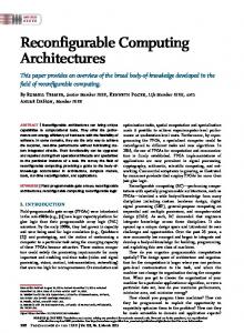
One of the big selling points of reconfigurable computing is its potential for supercomputer-like performance at modest cost, so designing a reconfigurable memory system based on low-cost off-the-shelf components is an important goal. The emerging high speed solutions for the interconnect fabric such as Arapahoe, Rapid I/O and HyperTransport differ widely not only in the technical specifications but also in their support by commercially available components. The HyperTransport point-to-point interconnect design [1], supporting bandwidths of up to 12.8 Gbytes per second, has been widely endorsed by industry. HyperTransport includes switching, tunnelling and emulation of older standards such as PCI. It has the advantage of having been adopted for mass-market PC designs from AMD, as well as by at least two different FPGA suppliers (Xilinx and Altera). Such a reconfigurable memory system should include capabilities of organizing memory into banks, and routing conflicting requests on non-conflicting paths through a network. A simple network-like topology is illustrated in Figure 1. In this design, each processing module would have a fast local memory, and would access a larger DRAM comprised of independent modules as a fast I/O device. The connection between processing modules and their local memory could be a common standard bus like that used for double-data rate (DDR) DRAM or SDRAM. On the FPGA chip, there would be faster local memory, forming the kind of hierarchy usual in conventional CPUbased designs.
Given then that we see bandwidth goals as more easily achievable than latency goals, does that mean we advocate the pursuit of latency over bandwidth in the design? No. The approach we advocate, again inspired by the IBM 3990 disk subsystem, is to minimize latency wherever we can by the structure of the design. Latency inherent in the devices cannot be wished away, but latency caused by contention for shared resources can be designed away. The approach we advocate is to design a network allowing alternative paths for competing requests which do not require the same resources. As opposed to a shared bus, this approach should minimize delays caused by contending for the interconnect. Clearly, we cannot hope to achieve the latency which would result from a fast SRAM integrated into the FPGA, or tightly coupled to the FPGA (e.g., in a multi-chip module). However, the kind of design we propose would be more general than such a design, and would save redesign time for each new configuration of a reconfigurable computer. Given that we would like to pursue low latency where possible, our design should include the option to route directly between processor or memory modules.
4.3 Static versus Dynamic Reconfiguration Since we are talking of a network, the question arises as to whether routing is static or dynamic, in the sense of
5
a
1
A
b
2
B
c
3
C
fast switches
DRAM modules
processing modules
fast memory
memory accordingly. A simple route such as {, , } would suffice for the main computation. However, information exchanges between processors would also be required. These could be routed through the memory or through the switches. Clearly, given the latency introduced by memory, routing through the switches would be the better option. To allow routes for all combinations, the interprocessor routes could look like this: 1.
{,,}
2.
{,,}
These routes allow a reasonable balance between a small number of dynamic choices and limited options for contention (e.g., processor a and b can communicate using interprocessor route 1, while processor c can be connected to its memory module 3 without contention). Examples of applications of this kind include wind tunnel simulations [4] and sintering [13].
Figure 1. A possible combination of processing and memory modules. The interconnect should provide more than one option for routing from a DRAM module to a processing module. The illustrated design shows switches, which could be used to reconfigure the topology. Processing modules will have a fast local memory, which may or may not be on-chip.
4.5.2 Varied Access Pattern
HyperTransport is a potential implementation framework for the planned reconfigurable memory architecture, because it has the required flexibility in design, and is aimed at relatively low-cost implementation, with relatively low board-level design cost.
In our second example, we assume that it is not possible to partition memory between processors as cleanly as in the first example. For such a scenario, we would like to have a range of different routes between processors and memory. For example, consider the following routes:
4.5 Putting it all Together: Examples Figure 1 suggests a general topology without suggesting how it may be used. An interconnect with fast switches could support dynamic reconfiguration. However, here we will only consider static reconfiguration. We will use the layout of Figure 1 to suggest alternative interconnect strategies. Routes are given as a set of , where X (capital letter) represents the memory module, n (number) the switch and y (lowercase letter) the processor. A processor-to-processor route would be given as y1ny2. We assume that any route is bi-directional (i.e., there is no difference between and ). If the switch required for a new route is busy, the request is queued at that switch. However, any switch which is not busy can be changed without waiting for queued requests at other switches to complete, provided that the new route does not conflict with and existing incomplete activity. We illustrate two scenarios to demonstrate the issues we need to address.
1.
{,,}
2.
{,,}
3.
{,,}
By switching between these three alternatives, it becomes possible for any memory module to be connected to any processor module. However, the route alternatives limit the combinations possible at one time. For example, if processor a were connected to memory module B (using route 3), the routes would have to be changed if processor b needed to be connected to memory module A (which requires route 2). 4.5.3 Summary The examples illustrate that a limited number of routes could cover a variety of cases, at least with a small-scale design. Our approach of supporting a limited number of statically designed routes selectable at run time will be sufficient for our initial prototype studies. We will work through more examples before finalizing design details such as the number of routes available to set up, and how runtime selection will work.
4.5.1 Fixed Access Pattern In our first example, the algorithm requires mainly nearest-neighbour interactions, with occasional exchanges of data. In this scenario, a viable strategy would be to split the workload between the processors, and to split the
6
5. Conclusions The design principles we have outlined here provide a basis for designing a reconfigurable memory system for reconfigurable computers. We believe that such a memory system will provide an important addition to the toolkit of reconfigurable computer designers. We aim that our design should prove to be sufficiently flexible, perform well enough to justify its use over a more specialized design and be low enough in cost to be of wide applicability. By basing our design principles on key ideas from a successful I/O subsystem, we are of the view that we will be able to meet the key design goals. To take our ideas forward, we plan to implement a prototype system with up to 4 FPGAs and a simple, statically reconfigurable interconnect. Based on this work, which will include simulation studies to predict future outcomes, we plan on extending the evaluation of the design to a larger project. To evaluate the design, we aim to implement at least two applications of sufficiently different memory requirements to demonstrate generality. Such generality will provide clear advantages for other implementers of reconfigurable computing.
[8]
[9]
[10]
[11] [12]
[13]
[14]
References
[15]
[1] AMD (2002). HyperTransport Technology: Simplifying System Design Available from http://www.hypertransport.org/docs/26635A_HT_System_ Design.pdf. [2] Bergmann, N. W. and Dawood (2001), A. S. Adaptive interfacing with reconfigurable computers. In Proc. 6th Australasian Conf. on Computer systems architecture, pages 11–18, Queensland, Australia. IEEE Computer Society Press. [3] Chen, S. and Postula (2000), A. Synthesis of Custom Interleaved Memory Systems. IEEE Transactions on VLSI Systems, 8(1): 74-83. [4] Cheriton, D.R., Goosen, H.A., Holbrook, H. and Machanick, P. (1993) Restructuring a Parallel Simulation to Improve Cache Behavior in a Shared-Memory Multiprocessor: The Value of Distributed Synchronization, Proc. 7th Workshop on Parallel and Distributed Simulation, May 1993, pages 159–162, San Diego, CA. [5] Compton, K. and Hauck, S (2002). Reconfigurable computing: a survey of systems and software. ACM Computing Surveys, 34(2): 171–210. [6] Crisp, R. (1997) Direct Rambus technology: The new main memory standard. IEEE Micro, 17(6): 18–28. [7] Cuppu, V., Jacob, B., Davis, B., and Mudge, T. (1999) Performance comparison of contemporary DRAM archi-
[16]
[17]
[18]
[19]
[20]
7
tectures. In Proc. 26th Annual Int. Symp. on Computer Architecture, pages 222–233, Atlanta, Georgia. Grossman, C.!P. (1992) Role of the DASD storage control in an Enterprise Systems Connection environment, IBM Systems Journal, 31(1): 123–146. Available from http://www.research.ibm.com/journal/sj/311/ibmsj3101M.p df. Hennessy, J. and Patterson, D. (2002) Computer Architecture: A Quantitative Approach. Morgan Kauffmann, San Francisco, CA, 3rd edition. Jacob, J. A. and Chow, P. (1999) Memory interfacing and instruction specification for reconfigurable processors. In Proc. 1999 ACM/SIGDA 7th Int. Symp. on Field Programmable Gate Arrays, pages 145–154, Monterey, California, United States. ACM Press. Johnson, E. (1995) Graffiti on the memory wall. Computer Architecture News, 23(4): 7–8. Ng, S., Lang, D. and Selinger, R. (1988) Trade-offs between devices and paths in achieving disk interleaving, Proc. 15th Annual Int.Symp.on Computer Architecture, pages 196–201, Honolulu, Hawaii. Postula, A., Abramson, D., and Logothetis, P. (1996) The design of a specialised processor for the simulation of sintering. In Proc. 22nd Euromicro Conf., Prague, Czech Republic. Seznec, A. and Lenfant, J. (1993) Odd memory systems may be quite interesting. In Proc. 20th Annual Int. Symp. on Computer Architecture, pages 341–350, San Diego, California, United States. Shing, H. and Ni, L. M. (1991) A conflict-free memory design for multiprocessors. In Proc. 1991 ACM/IEEE Conf. on Supercomputing, pages 46–55, Albuquerque, New Mexico, United States. Vuillemin, J.E., Bertin, P., Roncin, D., Shand, M., Touati, H., and Boucard, P. (1996) Programmable Active Memories: Reconfigurable Systems Come of Age. IEEE Transactions on VLSI Systems, 4(1): 56-69. Wigley, G. and Kearney, D. (2001) The first real operating system for reconfigurable computers. In Proc. 6th Australasian Conf. on Computer Systems Architecture, pages 130–137, Queensland, Australia. IEEE Computer Society Press. Wigley, G. and Kearney, D. (2002) The management of applications for reconfigurable computing using an operating system. In Proc. 7th Asia-Pacific Computer Systems Architecture Conf., pages 73–81, Monash University, Melbourne. Avail. from http://www.jrpit.flinders.edu.au/confpapers/CRPITV6Wigl ey.pdf. Wilton, S. J. E., Rose, J. and Vranesic, Z. G. (1999) The Memory/Logic Interface in FPGA's with Large Embedded Memory Arrays, IEEE Trans. on VLSI Systems, 7(1):80–91. Wulf, W. and McKee, S. (1995) Hitting the memory wall: Implications of the obvious. Computer Architecture News, 23(1): 20–24.