Scott A. McFarling, Steven A. Przybylski, Steve E. Richardson, Arturo Salz, Richard T. Simoni, Don C. Stark, Peter A. Steenkiste. Steve W.K. Tjiang, Malcolm J.
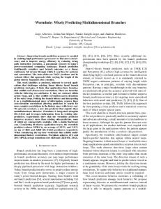
[See page 328 for Figure 1 .I
SESSION I I : 32b MICROPROCESSORS WAM 2.3
A 32b Microprocessor with OnChipZKbyte Instruction Cache Mark Horowitz, John L. Hennessy, Paul Chow, P. Glenn Gulak, JohnM . Acken, Anant Agarwal, Chorng-Yeung Chu, Scott A. McFarling, Steven A. Przybylski, Steve E. Richardson, Arturo Salz, Richard T. Simoni, Don C. Stark, Peter A. Steenkiste Steve W.K. Tjiang, Malcolm J. Wing Stanford University Center for Integrated Systems Stanford, CA
THE 32b MICROPROCESSOR to be described has an on-chip 2Kbyte instruction cache. The chip, implemented in a 2pm drawn channel length, 2-layer metal, N-well CMOS technology, contains 150K transistors in an 8mm x 8.5mm die, and has 8 4 signal pins and 24 power pins. With a nonoverlapping, Z-phase clock and a peak operating frequency of 20MHz the chip dissipates less than 1W. The microprocessor uses a simple instruction format that can be decoded quickly so that an instruction can be issued every cycle. All 37 instructions are 32b, and use a fixed format for the register specifiers. Like many other RISC machines’ ”, the microprocessor is a load/store machine. It avoids the high pin count or fast bus cycle times required to support fetching2 words per cycle (instruction and data) by using a large on-chip instruction cache. The cache reduces the off-chip instruction bandwidth by over a factor of 5 and the overall bandwidth by a factor of 2 to 2.5. The machine has a 5-stage pipeline: Instruction Fetch (IF), Register Fetch (RF), Execute (ALU), Memory access (MEM), and Write Back of registers (WB). During IF, the instruction address is fetched from the on-chip instruction cache. The RF cycle is used to drive the register specifiers from the Instruction Register to the register decoders and then to do theactual register fetch. During41 of the Execute pipestage for a branch instruction an adder in the program counter computes the branch destination, while the ALU computes the branch condition. For memory instructions the ALU is used t o compute the effective address, while for compute instructions theALU or shifter is used to compute thedesired result. The result of the ALU is driven onto the address pads during 42 of the Execute pipestage, giving the large external cache a full cycle (NEM) to complete its access. Finally, during WB a computer result or fetched data word is written to the register file. The pipeline forces two delay slots after a branch since the result of a branch is known only after the ALU cycle, too late to affect the IF of the next two instructions. T o help the software system utilize these slots the machine can optionally squash (or turn into noaps) the instructions in the slots if the branch does not go. ‘Rowen, C . , Przybylski, S . A . , Jouppi, N.P., Gross, T.R., Shott, J.D. and Hennessy, J.L., “ A Pipelined 32b NMOS Microprocessor”, I S S C C D I G E S T O F T E C H N I C A L P A P E R S , p. 180181: Feb., 1984. ’Sherburne, R.W.. Katevenis, M.G.H., Patterson, D.A. and Sequin, C.H., “A 32b NMOS Microprocessorwitha Large RegisterFile”, I S S C CD I G E S T O F T E C H N I C A LP A P E R S , P. 168-169:Feb.. 1984.
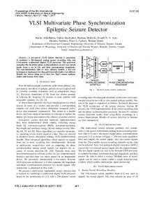
Die photo of the processor is shown in Figure 1. The cache is divided into 32 blocks of 16 words. The Tag unit contains the control logic for the cache, 512 valid bits and a small CAM for the 32 tags. By organizing the valid bit memory as 16 32b words, the valid bit access and CAM compare can occur simultaneously allowing the processor to determine quickly whether the cache hit. A cache miss causes the instruction and its successor to be fetched during the following two cycles. By using trace-driven simulations, the miss ratio has been measured to be about 12% onaverage. With an external cache miss ratio of 5%, this yields a sustained throughput of 1 2 MIPS on large benchmarks. The Register File contains a 32-word dual-ported file. 2 temporary and 2 bypass registers. The Execute unit contains a 32b funnel shifter,registers for multiplication/ division support, a 32b ALU, and the processor status word. The ALU uses a doubly-bypassed (by 4 and by 8 ) Manchester carry chain. The PC unit contains a branch displacement adder, an incrementer anda shift chain to save the PC values needed to restart the machine following an exception. The Instruction Register latches the cache output and sends partially decoded instructions to the datapath. The processor is controlled by two small finite state machines shown in Figure 3. One deals with squashing instructions, and the other handles internal cache misses. There are three situations that force an instruction to beconverted into a no-op: exceptions, squashed branches, and reset. The latter needs to no-op the instructions already in the pipe to guarantee the machine starts up in a deterministic way. These controllers use less than 0.27’0 of the total chip area. The only other control logic is secondary instruction decode. Features for testing the microprocessor include a pin that disables the on-chip cache and a pin that forces the chip into cache-test mode. In this state, the PC unit generates sequential addresses while the data bus is directly connected to the on-chip cache, allowing the cache to be directly read and written. Another pin forces test mode, which connects groups of the control lines directly onto the data pads. This pin can be asserted in the middle of any clock phase to observe the internal control state of the machine directly. Implementing this feature only requires a very small amount of logic which is placed under an existing bus? and does not increase the die size.
Acknowledgments The research effort was supported by the Defense Advanced Project Research Agency under Contract No. MDA903-83-C0335. P. Chow and G. Gulak were partially supported by the Natural Sciences and Engineering Research Council of Canada. The authors gratefully acknowledge J. Gasbarro and E. McCreight of Xerox for providing fabrication support.
Exception or Squashing Branch
ICacheTest Exception
(b) FIGURE 2-Finite state machines: (a-top)-squash state machine; (b-bottom)-cache miss finite statemachine.
FIGURE 2-Microprocessor die.