SIMULATION OF SEMICONDUCTOR PROCESSES AND DEVICES Vol. 12 Edited by T. Grasser and S. Selberherr - September 2007
49
Efficient Mask Design for Inverse Lithography Technology Based on 2D Discrete Cosine Transformation (DCT) Jinyu Zhang*, Wei Xiong*, Min-Chun Tsai○, Yan Wang* and Zhiping Yu* * Institute of Microelectronics, Tsinghua University, Beijing, China, 100084
[email protected] ○ Advanced Technology Group, Synopsys Inc., Mountain View, CA, 94043, USA Abstract An efficient algorithm is proposed for fast synthesis of low complexity model-based inverse lithography technology (ILT) and phase shift masks (PSM) to improve the resolution and pattern fidelity in optical microlithography. The patterns on the mask are transformed into frequency space using 2D discrete cosine transformation (DCT). The solution space is thus changed to frequency space from real space. By cutting off high frequency components in DC spectrum, the dimension of the solution space is greatly reduced. Using a gradient-based algorithm, we solve the inverse problem in incoherent and partial coherent imaging systems with binary, 6%EPSM and APSM mask. Good fidelity images are achieved.
1
Introduction
Resolution Enhancement Technologies (RETs) are widely used to cope with the severe optical distortions in sub-wavelength lithography. Pixelization based Inverse Lithography Technique (ILT) has been proposed [1] as an effective RET for subwavelength technology. It has long been known that the mask design can be achieved by considering the design of masks as an inverse problem. Using a rigorous mathematical approach, the inverse problem is solved to find the optimal mask for a given process. However, the problem is an ill-posed one; the optimal mask function is not unique, sometimes even has no solution. These issues can be addressed by recasting the inverse problem as an optimization problem. In the optimization process, the mask has been discretized M × N pixels to increases the degree-of-freedom in mask data manipulation. Then, the above inverse problem is equivalent to a nonlinear optimization in an M × N dimension solution space. Previous works [2-4] have been focused on improving algorithms to solve the problem within this large M × N space. In this paper, we propose a novel method which is able to reduce the dimension of the solution space significantly, based on discrete cosine transformation (DCT). We first transform the solution space from spatial domain to frequency domain. Then the dimension of solution space is reduced there. Also, a gradient-based algorithm is proposed to perform the optimization.
2
Details of Computation
We applied our method to three different mask technologies, i.e., binary, 6%EPSM (attenuated phase-shifting mask) and APSM (alternating phase shifting mask),
50
SIMULATION OF SEMICONDUCTOR PROCESSES AND DEVICES Vol. 12 Edited by T. Grasser and S. Selberherr - September 2007
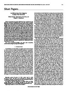
respectively. To demonstrate our method, we used a 40×40 discrete “double snake” pattern (shown in Fig. 1(a)), which is a typical layout of Metal 1 (M1) pattern. The pixel size is 25×25nm2 (1X), which is approximately equal to the minimal mask manufacturing size (100x100nm2 at 4X note: mask is 4x, and it is 100nm). The aerial image calculations are performed on the basis of incoherent and partial-coherent imaging system respectively. The resist effect is simulated using the constant threshold resist (CTR) [5] model. The patterns on the mask are transformed into frequency space using 2D discrete cosine transformation (DCT). Fig. 1(b) shows the DCT of “double snake pattern”. The solution space is thus in frequency space. We select a few hundred of low frequency DC components to construct solution space. Only the coefficients of these components are set to free parameters. By trimming high frequency components in DC spectrum, the dimension of the solution space is greatly reduced. For the coefficient of each DC component can be changed continuously, we are able to use gradient-based algorithms such as BFGS (Broyden, Fletcher, Goldfarb and Shanno) to perform the optimization.
(a) (b) Figure 1: (a) The desired pattern on wafer, and (b) the corresponding DCT matrix. The lighter colour pixels in (b) denote components with larger coefficient.
3
Results and Discussion
Fig. 2 shows the desired pattern and output intensity contour without RET for incoherent and partial-coherent system, respectively. To perform optimization, we used about 220 and 280 DC components for incoherent and partial-coherent system, respectively. The choice of number of DC components depends on convergence rate and optimization results. We found that, in a suitable solution space, it becomes possible to achieve the best convergence rate and good solution simultaneously. In the first beginning of optimization, the dimension of the DCT space could be roughly set to 1/5 of spatial space. The initial mask pattern is identical to the desired one. Fig. 3 shows the unmatched pixel number between the synthesis pattern on wafer and the desired one in each iteration. Figs 4-6 show the optimized mask and final image on wafer for incoherent image system binary mask, partial-coherence image system 6%EPSM and APSM mask, respectively. It can be seen that, using our algorithm, one can produce complex mask patterns to achieve good fidelity. These results indicate that, even in a much smaller DC solution space, good optimization can still be performed. It could be understood that the main frame of a graph is determined by its low frequency components and its high frequency
SIMULATION OF SEMICONDUCTOR PROCESSES AND DEVICES Vol. 12 Edited by T. Grasser and S. Selberherr - September 2007
51
components only decide the details which have trivial influences on final image quality on wafer.
. (a)
(b)
Figure 2: Desired pattern (solid) and output intensity contour without RET (dashed) in (a) incoherent and (b) partial-coherent imaging system.
(a)
(b)
Figure 3: The convergence process of (a) incoherent imaging system and (b) partialcoherent system, respectively.
4
Summary
An efficient ILT algorithm is proposed using pixel-based mask. Using DCT, the pattern on masks is transformed to frequency space, so is the solution space. By trimming the high frequency components, the solution space becomes much smaller. Using gradient-based algorithms, we solve the inverse problem in incoherent and partial-coherent imaging systems with binary, 6%EPSM, and APSM masks. Good fidelity images are achieved.
References [1] [2] [3]
B.E.A Saleh and S. I. Sayegh, "Reduction of errors of microphotographic reproductions by optimal corrections of original masks", Opt. Eng. 20, 781-787, 1981. Yong Liu and Avideh Zakhor, "Binary and phase-shifting mask design for optical lithography", IEEE Trans. Semicond. Manufact., 5, 138-152, 1992. Sherif Sherif and Bahaa Saleh, "Binary Image Synthesis Using Mixed Linear Integer Programming", IEEE Trans. Image Processing, 4, 1252-1257, 1995.
52
SIMULATION OF SEMICONDUCTOR PROCESSES AND DEVICES Vol. 12 Edited by T. Grasser and S. Selberherr - September 2007
[4]
Yuri Granik, "Solving Inverse Problems of Optical Microlithography", SPIE, 5754, 506526, 2005. W. Huang, et al., "Two threshold resist models for optical proximity correction", SPIE 5377, 1536–1543, 2001.
[5]
(a)
(b)
(a)
(b)
Figure 4: In incoherent model, (a) Optimized mask. White and black pixels have a transmission of 1 and 0 respectively. (b) Final image on wafer (dashed) and the desired pattern (solid).
Figure 5: In partial-coherent model, 6% EPSM mask. (a) Optimized mask. White and black pixels have a transmission of 1 and -0.245 respectively. (b) Final image (dashed) on wafer and the desired pattern (solid) .
(a)
(b)
Figure 6: In partial-coherent model, APSM mask. (a) Optimized mask. White, grey and black pixels have a transmission of 1, 0 and -1 respectively. (b) Final image on wafer (dashed) and the desired pattern (solid).