APPLIED PHYSICS LETTERS 91, 052507 共2007兲
Spin transfer switching in current-perpendicular-to-plane spin valve observed by magneto-optical Kerr effect using visible light Ken-ichi Aoshima,a兲 Nobuhiko Funabashi, Kenji Machida, Yasuyoshi Miyamoto, Norikazu Kawamura, Kiyoshi Kuga, Naoki Shimidzu, and Fumio Sato Science & Technical Research Laboratories, Japan Broadcasting Corporation, 1-10-11 Kinuta Setagaya, Tokyo 157-8510, Japan
Takashi Kimura and Yoshichika Otani The Institute for Solid State Physics, The University of Tokyo, 5-1-5 Kashiwanoha, Kashiwa Chiba 277-8581, Japan
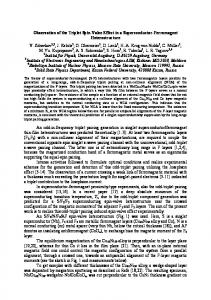
共Received 20 April 2007; accepted 10 July 2007; published online 2 August 2007兲 The authors have succeeded in optically observing the spin transfer switching 共STS兲 in a current-perpendicular-to-plane spin-valve device. The device consists of three spin-valve elements, each of which comprises of a transparent top electrode, free and pinned magnetic layers separated by a copper spacer, and a bottom copper electrode. Despite a relatively large device resistance, spin transfer switching of the free layer was carried out using the spin injection from the transparent top electrode. Magneto-optical Kerr effect measurements performed through the transparent top electrode show clear changes in the signal synchronized with the resistance change as a result of the STS. © 2007 American Institute of Physics. 关DOI: 10.1063/1.2767770兴 The spin transfer switching 共STS兲 technique has remarkably progressed1–4 since its theoretical prediction5,6 and the experimental confirmation.1 Recently, the detailed magnetization switching process in the current-perpendicular-toplane 共CPP兲 spin-valve device has been directly observed by using a time resolved x-ray microscopy7 while the switching of the nanomagnetic element has been examined by taking simultaneous measurements of the resistance change of the device. Unlike the above x-ray microscopy, the magnetooptical Kerr effect 共MOKE兲 microscopy is an easily accessible method to observe the switching process. However, a thick metallic top electrode usually prevents the light probing the magnetic free layer. We have fabricated submicron CPP spin-valve devices that have transparent top electrodes, which enable us to optically monitor the STS of the free layer. The obtained results clearly show that the change in magnetoresistance 共MR兲 caused by the STS, coincide well with that of the MOKE signal. A schematic drawing of the fabricated spin-valve device is shown in Fig. 1. The spin valve contains a bottom electrode of 关Ta共3兲 / Cu共50兲 / Ta共3兲 / Cu共50兲 / Ru共5兲兴, a synthetic pinned layer of 关Ru共5兲 / Cu共20兲 / Ir22Mn78共10兲 / Co66Fe34共5兲 / Ru共0.9兲 / Co66Fe34共1兲 / Co2FeSi共10兲兴, Cu spacer of 关Cu共6兲兴 and a free layer with capping of 关Co2FeSi共6兲 / Cu共3兲 / Ru共3兲兴 共in nanometers兲, which were deposited on a thermally oxidized Si substrate using a dc magnetron sputtering system. After annealing at 300 ° C in a vacuum less than 1 ⫻ 10−4 Pa, three rectangular elements of 120⫻ 300 nm2 were fabricated on a same bottom electrode using electron beam lithography, followed by Ar ion beam milling, SiO2 insulator deposition, and a lift-off process. The indium zinc oxide 共IZO兲 top electrode of 500 nm was then deposited using an ion beam sputtering system. The MR loop was measured at room temperature using a four-point probe system. The STS characteristics were then evaluated by applying a pulsed current with a duration of 5 ms variable in a兲
Electronic mail:
[email protected]
the range from −30 to + 30 mA with an increment of 2 mA without applied magnetic field. To measure the change in MOKE signal associated with it, a longitudinal MOKE measurement system8 with a laser spot diameter of about 1.6 m and a wave length of 405 nm was synchronized with the STS 共Fig. 1兲. An optical microscope image of the fabricated device and an atomic force microscope image of the constituent spin-valve elements are shown in Figs. 2共a兲 and 2共b兲. The rectangles indicated by the dashed line show the elements, each of which is 120⫻ 300 nm2. The device is 720 ⫻ 300 nm2 including the space between horizontal lines. Therefore, the laser spot can be well aligned with the device for efficient MOKE signal detection even though the element is much smaller than the laser spot of 1.6 m. Transparency and low electrical resistance of the top electrode are crucial to both MOKE and STS measurements.
FIG. 1. Schematic illustration of spin-valve device with transparent top electrode, and experimental setup. The plain arrow in the free layer indicates the direction of the magnetization. The device includes the bottom electrode of 关Ta共3兲 / Cu共50兲 / Ta共3兲 / Cu共50兲 / Ru共5兲兴, the pinned layer of 关Ru共5兲 / Cu共20兲 / Ir22Mn78共10兲 / Co66Fe34共5兲 / Ru共0.9兲 / Co66Fe34共1兲 / Co2FeSi共10兲兴, an intermediate layer of Cu共6兲, and the free layer with capping of 关Co2FeSi共6兲 / Cu共3兲 / Ru共3兲兴, all in nanometers.
0003-6951/2007/91共5兲/052507/3/$23.00 91, 052507-1 © 2007 American Institute of Physics Downloaded 10 Aug 2007 to 157.82.227.2. Redistribution subject to AIP license or copyright, see http://apl.aip.org/apl/copyright.jsp
052507-2
Aoshima et al.
Appl. Phys. Lett. 91, 052507 共2007兲
FIG. 2. 共Color online兲 共a兲 Optical microscopy image of CPP-spin-valve device. Center dot indicates laser spot for MOKE detection. 共b兲 Atomic force microscopy image of three spin-valve elements. Rectangles indicated by the dashed line show the spin-valve elements, each of which is 120 ⫻ 300 nm2. The device is 720⫻ 300 nm2 including the space between the horizontal lines.
The optical properties of candidate materials, IZO 共500 nm thick兲 and thin Cu 共10 nm thick兲 films, were thus examined in the 350– 800 nm wavelength range. The transparency of IZO was about 65%–80%, larger than that of the 10-nm-thick Cu for most of the visible spectra. The resistances of the devices with the IZO, and with 10- and 500-nm-thick Cu top electrodes are shown in Fig. 3. It is important to note that the device with the 500-nm-thick IZO electrode shows smaller resistance than that with the 10-nm-thick Cu top electrode even though the resistivity of Cu is much lower than that of IZO. Another significant point is that the in-plane resistance of the top electrode tends to contribute to the total device resistance because of the very small resistance of all metal CPP elements. This is why the device with the 10-nm-thick Cu top electrode exhibits larger device resistance than those with IZO and Cu top electrodes 500 nm thick. These results confirm that both the optical and electrical properties of the IZO top electrode are better than those of Cu electrode. The resistance of the transparent electrode makes the net device resistance about seven times larger than that of the conventional device with a 500-nm-thick Cu top electrode. One should note here that the MR property evaluated as the change in resistance ⌬R between antiparallel 共AP兲 and parallel 共P兲 magnetic configurations of free and pinned layers remains the same irrespective of the large top electrode resistance. The STS characteristics of the device, i.e., resistance as a function of the applied
FIG. 4. 共a兲 STS and the 共b兲 Kerr ellipticity characteristics for three spinvalve elements. Open circles in 共a兲 indicate resistance as a function of the applied current of ±30 mA with an increment of 2 mA. 共b兲 The changes are defined as 关K − 具K典兴 in Kerr ellipticity for various applied currents of −3, −25, +3, and +30 mA. Kerr measurements are synchronized with resistance measurements 关solid squares in 共a兲兴. Averaged values over 60 points at each four different currents are plotted with error bars of standard deviation.
current 共R-I curve兲, where several steps are observed in the resistance change ⌬R, are shown in Fig. 4共a兲. The STS current seems different among the three elements as a result of the size distribution caused by the lithography error, and nonidentical domain structures in the free layers of the elements. Relatively large jumps at −8, −20, +10, and +14 mA correspond to complete switching of the two free layers in the three elements, respectively. Two other small jumps, one at −4, and another at +30 mA correspond to partial switching of a remaining element. Full switching of all free layers by external magnetic field yields a resistance change of 0.035 ⍀ 共not shown兲, while the STS yields only 0.030 ⍀. This incompleteness may be attributed to an inhomogeneous current path. However, most of the free layers, switch at below 30 mA 共2.78⫻ 107 A / cm2兲, which is in good agreement with the tendency observed in the device with a thick Cu top electrode,9 indicate that the resistive transparent electrode shows the switching capability similar to that of the thick Cu electrode. Resistance and Kerr ellipticity 共K兲 of the device are measured simultaneously after each current injection of I = −3, −25, +3, and +30 mA, which sets the magnetic state of the device in AP, P, P, and AP configurations, respectively. The results are plotted in Fig. 4共a兲 with solid squares that coincide well with the R-I curve. This indicates that the switching completes in the cycle, although a small base line shift occurs as a result of a change in the contact resistance
FIG. 3. 共Color online兲 Device resistance as a function of lateral size of the devices with the top electrode of the IZO of 500 nm, and Cu of 10 and 500 nm thickness. Downloaded 10 Aug 2007 to 157.82.227.2. Redistribution subject to AIP license or copyright, see http://apl.aip.org/apl/copyright.jsp
052507-3
Appl. Phys. Lett. 91, 052507 共2007兲
Aoshima et al.
of interconnections. The average values of a Kerr ellipticity change determined as 关K − 具K典兴 for each injection current are plotted with error bars of standard deviation in Fig. 4共b兲. This clearly indicates that the Kerr ellipticity modulation is synchronized with the spin transfer switching. The Kerr ellipticity change 共⬃0.63⫻ 10−4 deg兲 that was detected was reduced to 6% of that of the free layer film 共1.08⫻ 10−3 deg兲. This reduction could be explained by the small lateral size of the device 共the magneto-optically active area兲, which is about 5% of the laser spot area. This quantitative consistency supports the MOKE results. This device concept with large MOKE materials may open up applications such as an optical analysis on the dynamics of free layer switching and a submicron MO spatial light modulator 共MOSLM兲 which may have a significant impact for holographic applications.10,11 However, the MOKE signal from the Co2FeSi free layer of this device is not enough for these applications. There are some large MOKE materials that may meet the requirements of the applications. For example, Co/ Pt multilayer,12 of which STS has been observed,13 shows a Kerr rotation that is 70 times larger 共about 0.4°兲 than that shown in the Co2FeSi 共0.006°兲. Also, the MnBiAl alloy shows a Kerr rotation of 3.2° 共Ref. 14兲 which is not far from a practical requirement of the Kerr rotation 共8°兲 for the MOSLM,15 although the STS properties have not yet been examined. In conclusion we have fabricated current-perpendicularto-plane spin-valve devices with transparent top electrodes, which enable us to optically observe the magnetic state of the free layers. We carried out spin transfer switching by
current injection from the transparent electrode despite the relatively large resistance of the device. Clear change in the Kerr ellipticity was observed by changing the direction of magnetization of the free layers using spin transfer switching. 1
E. B. Mayer, D. C. Ralph, J. A. Katine, R. N. Louie, and R. A. Buhrman, Science 285, 867 共1999兲. 2 J. A. Katine, F. J. Albert, R. A. Buhrman, E. B. Myers, and D. C. Ralph, Phys. Rev. Lett. 84, 3149 共2000兲. 3 K. Yagami, A. A. Tulapurkar, A. Fukushima, and Y. Suzuki, Appl. Phys. Lett. 85, 5634 共2004兲. 4 Z. Diao, D. Apalkov, M. Pakala, Y. Ding, A. Panchula, and Y. Huai, Appl. Phys. Lett. 87, 232502 共2005兲. 5 J. C. Slonczewski, J. Magn. Magn. Mater. 159, L1 共1996兲. 6 L. Berger, Phys. Rev. B 54, 9353 共1996兲. 7 Y. Acremann, J. P. Strachan, V. Chembrolu, S. D. Andrew, T. Tyliszczak, J. A. Katine, M. J. Carey, B. M. Clemens, H. C. Siegmann, and J. Stoehr, Phys. Rev. Lett. 96, 217202 共2006兲. 8 K. Akahane, T. Kimura, and Y. Otani, J. Magn. Soc. Jpn. 28, 122 共2004兲 关in Japanese兴. 9 K. Aoshima, N. Funabashi, K. Machida, Y. Miyamoto, K. Kuga, and N. Kawamura, J. Magn. Magn. Mater. 310, 2018 共2007兲. 10 T. Mishina, M. Okui, and F. Okano, Appl. Opt. 41, 1489 共2002兲. 11 N. Ishii, T. Muroi, N. Kinoshita, K. Kamijo, and N. Shimidzu, Proc. SPIE 6488, 64880G 共2007兲. 12 P. F. Carcia, J. Appl. Phys. 63, 5066 共1988兲; S. Hashimoto, Y. Ochiai, and K. Aso, Jpn. J. Appl. Phys., Part 2 28, L1824 共1989兲. 13 H. Meng and J. Wang, Appl. Phys. Lett. 88, 172506 共2006兲. 14 C. Shang, Y. Wang, L. Chen, H. Zhang, and J. Liu, J. Appl. Phys. 81, 5662 共1997兲. 15 J. Park, H. Takagi, J. Cho, K. Nishimura, H. Uchida, and M. Inoue, IEEE Trans. Magn. 40, 3045 共2004兲; J. Park, J. Cho, K. Nishimura, and M. Inoue, Jpn. J. Appl. Phys., Part 1 41, 1813 共2002兲.
Downloaded 10 Aug 2007 to 157.82.227.2. Redistribution subject to AIP license or copyright, see http://apl.aip.org/apl/copyright.jsp