American Journal of Materials Science and Engineering, 2014, Vol. 2, No. 2, 13-17 Available online at http://pubs.sciepub.com/ajmse/2/2/1 © Science and Education Publishing DOI:10.12691/ajmse-2-2-1
Structural and Optical Properties of Different Composition of Se90Cd10-xInx thin Films by Vacuum Evaporation Technique D.K. Dwivedi1,*, Nitesh Shukla1, H.P. Pathak1, Kedar Singh2 1
Amorphous Semiconductor Research Lab, Department of Physics, Madan Mohan Malaviya University of Technology, Gorakhpur 2 Department of Physics, Banaras Hindu University, Varanasi *Corresponding author:
[email protected]
Received April 18, 2014; Revised April 23, 2014; Accepted April 27, 2014
Abstract Se90Cd10-xInx (x=2,4,6 &8) thin films have been deposited onto a chemically cleaned glass substrate by thermal evaporation technique under vacuum. The effects of different doping concentration of In have been investigated X-ray diffraction technique has been employed to investigate the structural characterization of the films. X-ray diffraction measurement indicates that the Se90Cd10-xInx films possess polycrystalline structure. Absorption spectra measured at normal incidence in the wavelength range 400-1100 nm have been analyzed for the optical characterization of the thin films under consideration. The optical constants (absorption coefficient (α), extinction coefficient (k)) and optical band gap Eg have been calculated. The absorption coefficient (α) is found to increase with photon energy. It has been found that extinction coefficient (K) decreases with increase in wavelength (λ). Optical band gap (Eg) has also been evaluated for the Se90Cd10-xInx thin films with different compositions. It has been found that optical band gap (Eg) increases with In incorporation in Se90Cd10-xInx alloys.
Keywords: Chalcogenide glasses, amorphous semiconductors, thin films, optical properties, optical band gap Cite This Article: D.K.Dwivedi, Nitesh Shukla, H.P. Pathak, and Kedar Singh, “Structural and Optical Properties of Different Composition of Se90Cd10-xInx thin Films by Vacuum Evaporation Technique.” American Journal of Materials Science and Engineering, vol. 2, no. 2 (2014): 13-17. doi: 10.12691/ajmse-2-2-1.
1. Introduction Among Chalcogenide glassy semiconductors the II-VI compound semiconductors are extremely vibrant because of their uses in the optoelectronic devices and solar cells [1-10]. These materials particularly Se glasses exhibit unique property of reversible transformation [11]. This property makes these glasses very useful in optical memory devices [12,13,14]. Se based Chalcogenide glasses have high transparency in the broad middle and far infrared region and have strong nonlinear properties [15]. Though amorphous Se has got various device applications which make it attractive but pure Se has disadvantage like short life time and low sensitivity. This problem can be overcome by alloying Se with some impurity atoms, which gives higher sensitivity, higher crystallization temperature and smaller aging effect [16,17,18]. In the present work In has been chosen as an additive element in Se-Cd matrix to prepare Se-Cd-In alloys, because it is recognized as one of the most efficient elements used to improve the opto-electronic properties of compounds [19]. The third element behaves as chemical modifier and creates compositional as well as configurational disorder in the material with respect to binary alloys, which will be useful in understanding the structural, electrical and optical properties of Se-Cd-In chalcogenide glasses
[20,21,22]. Se-Cd-In is a semiconductor ternary chalcogenide glass of the type AVIBIICIII, where A = Se, Te, S, B = Cd, Zn and C=In, Tl, Ga. The ternary chalcogenides have potential applications in solar energy conversion due to their interesting tailored properties [23-28], in optoelectronic devices [29] and in nonlinear optics [30,31]. A number of techniques have been employed to prepare semiconductor ternary chalcogenide glasses of the type AVIBIICIII including sputtering, physical vapor deposition, thermal evaporation method, spray pyrolysis and electro deposition technique [32-37]. In the present work resistive thermal evaporation method has been used due to considerably large mean free path of the vapor atoms at low pressure and a sharp thin film is obtained. This technique provides a wide window for the selection of substrate with minimum impurity concentration in the film. In the present work our aim is to study the effect of In incorporation on the structural and optical properties of Se-Cd matrix. X-ray diffraction technique has been employed to investigate the structural properties of the Se90Cd10-xInx alloys. The optical behavior of a material is utilized to determine its optical constants. Therefore, an accurate measurement of optical constants is extremely important. Optical absorption spectra of Se90Cd10-xInx (x = 2, 4, 6 & 8) thin films have been recorded in the wavelength range 400-1100 nm by double beam UV-Vis spectrophotometer. Optical parameters like absorption
14
American Journal of Materials Science and Engineering
coefficient (α), extinction coefficient (k) and optical band gap (Eg) have been calculated for Se90Cd10-xInx alloys.
2. Experimental Alloys of Se90Cd10-xInx (x = 2, 4, 6 & 8) were prepared by melt quenching technique. The exact proportions of high purity (99.999%) Se, Cd and In elements, in accordance with their atomic percentages, were weighed using an electronic balance (LIBROR, AEG-120) with the least count of 10-4 gm. The material was then sealed in evacuated (~10-5 Torr) quartz ampoule (length ~ 5 cm and internal diameter ~ 8 mm). The ampoule containing material was heated to 800 0C and was held at that temperature for 12 hours. The temperature of the furnace was raised slowly at a rate of 3 - 4°C / minute. During heating, the ampoule was constantly rocked, by rotating a ceramic rod to which the ampoule was tucked away in the furnace. This was done to obtain homogeneous alloy. After rocking for about 12 hours, the obtained melt was rapidly quenched in ice-cooled water. The quenched sample was then taken out by breaking the quartz ampoule. Thin films of Se90Cd10-xInx (x = 2, 4, 6 & 8) were prepared by vacuum evaporation technique, in which the substrate was kept at room temperature at a base pressure of 10-6 Torr using a molybdenum boat. The films were kept inside the deposition chamber for 24 hours to achieve the metastable equilibrium as suggested by Abkowitz [38]. The thickness of the film was measured using a single crystal thickness monitor. The XRD patterns of the films were recorded with the help of x-ray diffractometer (XPERT-PRO) using Cu-Kα radiation (λ=1.54 Å). The tube was operated at 45 kV and 35 mA. The normal incidence absorption spectra of Se90Cd10-xInx (x = 2, 4, 6 & 8) thin films have been taken by a double beam UVVis-NIR computer controlled spectrophotometer (ECILHyderabad, India, Model No.5704 SS) in the wave length range 400-1100 nm.
D = 0.9λ / β Cosθ
(2)
Where β is full width at half maximum (FWHM) in radians, λ is the wavelength of X-rays used and θ is the Bragg’s angle. The strain (ϵ) has been evaluated using the formula
= β Cosθ / 4
(3)
The dislocation density (δ), defined as the length of dislocation lines per unit volume of the crystal is evaluated from the formula [38]
δ = 15β Cosθ / 4aD
(4)
Where D is the crystallite size, β is the full width at half maximum,θ is the Bragg’s angle and a is the lattice parameter. The microstructural parameters such as crystallite size (D), strain (ϵ), dislocation density (δ) and the lattice parameter values have been evaluated using above equations and the results are listed in Table 1. As the In dopant concentration increases the crystallite size decreases. This happens because In doping causes broadening of (100) peak, corresponding to a decrease of crystallite size of the films. The dislocation density estimated using Eq.(4), increases with increase in the In doping concentration which may be related to the increase in lattice dislocation due to the increase in doner sites. These observations match with the earlier results reported on Se-Cd-In thin films [38].
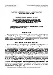
3. Results and Discussion 3.1. Structural Property Figure 1 shows the XRD pattern of Se90Cd10-xInx (x = 2, 4, 6 & 8) thin films. X-ray diffraction pattern reveal that the Se90Cd10-xInx thin films are polycrystalline in nature. For Se90Cd10-xInx thin films, the peaks at 2θ=23.6º, 2θ=25.5º,2θ=29.8º, 2θ=43.4º reveal the existence of (100),(002),(101) and (110) diffraction peaks which corresponds to hexagonal structure [22,39,40]. It has been observed that the intensity of all peaks increases significantly with the incorporation of In in Se-Cd alloys. A comparison of the observed and standard d values for (hkl) planes ensures that Se90Cd10-xInx (x=2, 4, 6&8) show hexagonal structure [41]. The lattice parameters of the hexagonal planes are calculated using the following relationship
= 1/ d
( 4 / 3) [(h 2 + k 2 + 2 ) / a 2 ] + ( 2 / c2 )
(1)
The values of lattice parameters for Se90Cd10-xInx thin films are listed in Table1. The crystallite size D has been estimated by using the Debye-Scherer’s formula [39]
Figure 1. XRD pattern of Se90Cd10-xInx (x=2, 4, 6&8) thin films Table 1. Microstructural parameters of Se90Cd10-xInx thin films Lattice Crystallite Dislocation parameters Strain In doping density size D (nm) concentration ϵ×10-3 δ×1015(lines m-2) (nm) a c X=2 26.22 1.70 1.33 4.34 3.76 X=4 17.40 3.97 1.99 4.34 -X=6 14.40 5.80 2.40 4.34 -X=8 13.92 6.20 2.49 4.34 --
American Journal of Materials Science and Engineering
3.2. Optical Properties 3.2.1. Absorption Coefficient (α) and Optical Band Gap (Eg) The absorption coefficient (α) has been obtained directly from the absorbance against wavelength curves using the relation [42-50].
α = OD / t
(5)
Where OD is the optical density measured at a given layer thickness (t). A plot of absorption coefficient (α) as a function of photon energy (hν) is given in Figure 2 and values are given in Table 2. It has been observed that absorption coefficient (α) increases with increase in photon energy (hν). Absorption coefficient (α) decreases with increase in concentration of In in Se-Cd-In matrix.
15
and the value of optical band gap. The relation between absorption coefficient (α) and the incident photon energy (hν) be written as [51].
(α hν= )1/n
(
A hν − E g
)
(6)
where, A is the edge width parameter representing the film quality, which is calculated from the linear part of this relation and Eg is the optical band gap of the material. The exponent n depends on the type of transition. For direct allowed n=1/2, indirect allowed transition n=2 and for direct forbidden n=3/2. To determine the possible transition (αhν)1/n vs hν is plotted and corresponding Eg values are obtained by extrapolating the straight line portion of the graph on hν axis as shown in figure 3.
Figure 3. Variation of (αhν)2with (hυ) in Se90Cd10-x Inx (x = 2,4,6 & 8) thin films
.
Figure 2. Variation of absorption coefficient (α) with photon energy (hν) in Se90Cd10-xInx (x=2, 4, 6&8) thin films Table 2. Optical band gap (Eg), absorption coefficient (α) and extinction coefficient (k) for Se90Cd10-xInx thin films Optical Absorption Extinction S.No. Sample Band Gap Coefficient (α) Coefficient (Eg) in eV (cm-1)×103 (k) 10-2 1. Se90Cd8In2 1.67 5.7050 0.3950 2. Se90Cd6In4 1.95 5.1820 0.3380 3. Se90Cd4In6 2.50 4.8625 0.3093 4. Se90Cd2In8 2.80 4.6250 0.3089
Large amount of dopants induces a large free carrier density in the bands and a high density of ionized dopants ions which cause the formation of band tails and variation of density of states, which strongly influence the optical properties. In defect free crystalline semiconductors, an energy gap is clearly defined because the conductor and valence band distribution of states terminate abruptly at their respective band edges. But presence of tail states in doped semiconductor makes it difficult to give a realistic energy gap value for these materials. One of the standard empirical method to obtain the optical gap values is the Tauc method. The fundamental absorption, which corresponds to electron excitation from the valence band to conduction band, can be used to determine the nature
The direct optical band gap values calculated from (αhν)2 vs hν are listed in Table 2. It is evident from Table 2 that the values of optical band gap(Eg) increases with increasing In concentration. It has been observed from XRD that crystallite size decreases with increases in In doping concentration, therefore the increase in band gap values with the increasing doping concentration may be attributed to size quantization. Variation of optical band gap (Eg) with In concentration in Se90Cd10-xInx (x=2,4,6&8) alloys is shown in Figure 4.
Figure 4. Variation of optical band gap (Eg) with In concentration in Se90Cd10-x Inx (x = 2, 4, 6 & 8) thin films
16
American Journal of Materials Science and Engineering
3.2.2. Extinction Coefficient (k)
Acknowledgement
The optical behavior of the material has been utilized to determine its extinction coefficient (k). The extinction coefficient has been calculated using the relation
k = αλ / 4π
(7)
Where α is optical density/film thickness Figure 5 shows the spectral dependence of k for Se90Cd10-xInx (x = 2, 4, 6 & 8) thin films. It is clear from the figure that k decreases linearly with an increase in λ for all the samples. This behavior is due to decrease in absorption coefficient with increase in λ. It is also evident from Table 2 that k decreases with In concentration in Se90Cd10-xInx thin films.
The authors are very much grateful to the University Grants Commission (UGC), New Delhi, India for providing financial assistance in form of major research project F.No. 39-452/2010 (SR). The authors also thank Prof. Ashok Kumar and Dr. R.K. Shukla, Department of Physics, H.B.T.I., Kanpur for fruitful suggestions.
References [1]
[2]
[3]
[4] [5]
[6] [7] Figure 5. Variation of extinction coefficient (k) with wavelength (λ) in Se90Cd10-xInx (x = 2, 4, 6 & 8) thin films
[8]
4. Conclusion
[9]
Thin films of Se90Cd10-xInx (x = 2, 4, 6 & 8) alloys have been deposited onto a chemically cleaned glass substrate by thermal evaporation technique. An attempt has been made to understand the effect of Indium doping concentrations on the structural and optical properties of Se-Cd-In thin films. XRD measurement indicates that Se90Cd10-xInx thin films are polycrystalline in nature and possess hexagonal structure. Crystallinity increases with the increase of In incorporation in Se-Cd alloys. The optical absorption spectra of Se90Cd10-xInx alloys have been studied in the wavelength range of 400-1100 nm by spectrophotometer. The optical parameters like absorption coefficient (α), extinction coefficient (k) and optical band gap (Eg) have been calculated for Se90Cd10-xInx alloys. It is observed that extinction coefficient (k) decreases with wavelength (λ) for all the samples. Absorption coefficient (α) is found to increase linearly with incident photon energy (hν) for all the samples. It has further been observed that both k and α decreases with increasing In concentration in Se-Cd matrix. Absorption measurement show the presence of direct band gap for Se90Cd10-xInx thin films and the band gap increases as the In dopant concentration increases. The increase in band gap values with increasing In doping concentration may be due to the effect of size quantization.
[10] [11] [12] [13]
[14] [15]
[16] [17]
[18] [19]
Mahalingam, T., Kathalingam, A., Velumani, S., Soonil Lee, Kyeung Seek Lew and Yong Deak Kim, “Characterization of electrodeposited Zn1−xHgxSe thin films”,Semicond. Sci. Technol., 20, 749-754, 2005. Tenne, Reshef, Mirovsky, Yehudith, Greenstein, Yaàcov and Giriat W., “Ternary Chalcogenide-Based Photoelectrochemical Cells: VII. Analysis of the Chemical Processes Occurring at the Surface during Photoelectrochemical Operation”, J. Electrochem. Soc, 132, 1829-1835, 1985. Choe, Sung-Hyu, Park, Bok-Nam, Xi-Yu-Su, Oh, Se- Jung, Park, Hong- Lee and Kim, Wha-Tek, “Optical properties of undoped and Co-DOPED CdIn2Se4 single crystals”, J. Phys. Chem. Solids, 56, 89-92, 1995. Mahapatra, P.K. and Dubey, A.R., “Photo electrochemical behaviour of mixed polycrystalline n-type CdS-CdSe electrodes”, Sol. Energy Mater. Sol. Cells, 32(1), 29-35, 1994. Masumdar, E.U., Gaikwad, V.B., Pujari, V.B., More, P.D. and Deshmukh, L.P., “Some studies on chemically synthesized antimony-doped CdSe thin films”, Mater. Chem. Phys., 77 (3), 669-676, 2003. Shahane, G.S. and Deshmukh, L.P., “Structural and electrical transport properties of CdS0.9Se0.1:in thin films: effect of film thickness”, Mater. Chem. Phys., 70 (1), 112-116, 2001. Hankare, P.P., Bhuse, V.M., Garadkar, K.M., Delekar, S.D. and Mulla, I.S., “Chemical deposition of cubic CdSe and HgSe thin films and their characterization”, Semicond. Sci. Technol., 19(1), 70-75, 2004. Murali, K.R., Swaminathan, V. and Trivedi, D.C., “Characteristics of nanocrystalline CdSe films”, Sol. Energy Mater. Sol. Cells, 81 (1), 113-118, 2004. Choi, J.Y., Kim, K.J., Yoo, J.B. and Kim, D., “Properties of cadmium sulfide thin films deposited by chemical bath deposition with ultrasonication”, Solar Energy, 64(1-3), 41-47, 1998. O’Brien, P. and McAleese, J., “Developing an understanding of the processes controlling the chemical bath deposition of ZnS and CdS”, J. Mater. Chem., 8, 2309-2314, 1998. Tanaka, K., “Structural phase transitions in Chalcogenide glasses”, Phys. Rev. B, 39, 1270-1279, 1989. Shimizu, A., “Data Detection using Pattern Recognition for Multilevel Optical Recording”, Technical Digest of ISOM 2001, 300301, 2001. Akiyama, T., Uno, M., Kituara, H., Narumi, K., Nishiuchi, K. and Amada, N., “Rewritable Dual-Layer Phase-Change Optical Disk Utilizing a Blue-Violet Laser”, Jpn J. appl. Phys., 40, 1598-1603, 2001. Ohta, T., “Phase-change optical memory promotes the DVD optical disk”, J. Optoelectron. Adv. Mater., 3, 609-626, 2001. Harbold, J.M., Hilday, F.O., Wise, F.W. and Itkain, B.G., “Highly nonlinear Ge-As-Se and Ge-As-S-Se glasses for all-optical switching”, IEEE Photonics Technology Letters, 14(6), 822-824, 2002. Shimakawa, K., “Residual photocurrent decay in amorphous Chalcogenides”, J Non-Cryst Solids, 77-78, Part 2, 1253-1256, 1985. Shim, Jae Yeob, Park, Sang Wook and Baik, Hong Koo, “Silicide formation in cobalt/amorphous silicon, amorphous Co_Si and bias-induced Co_Si films”, Thin Solid Films, 292 (1-2), 31-39, 1997. Saiter, J.M, Ledru, J., Hamou, A. and Saffarini, G., “Crystallization of AsxSe1−x from the glassy state (0.005