Structural, Electronic and Phononic Properties of PtSe2 : from Monolayer to Bulk A. Kandemir,1, ∗ B. Akbali,2 Z. Kahraman,3 S. V. Badalov,3 M. Ozcan,3 F. Iyikanat,2 and H. Sahin3, 4 1
Department of Materials Science and Engineering,
Izmir Institute of Technology, 35430, Izmir, Turkey 2 3
Department of Physics, Izmir Institute of Technology, 35430, Izmir, Turkey
Department of Photonics, Izmir Institute of Technology, 35430, Izmir, Turkey 4
ICTP-ECAR Eurasian Center for Advanced Research, Izmir Institute of Technology, 35430, Izmir, Turkey
Abstract The layer dependent structural, electronic and vibrational properties of the 1T phase of two dimensional (2D) platinum diselenide are investigated by means of state-of-the-art first-principles calculations. Main findings of the study are (i) monolayer platinum diselenide has a dynamically stable 2D octahedral structure with 1.66 eV indirect band gap, (ii) semiconducting nature of 1TPtSe2 monolayers remains unaffected even at high biaxial strains, (iii) top-to-top (AA) arrangement is found to be the energetically the most favorable stacking of 1T-PtSe2 layers, (iv) lattice constant (layer-layer distance) increases (decreases) with increasing number of layers, (v) while monolayer and bilayer of 1T-PtSe2 are indirect semiconductors, bulk and few-layered 1T-PtSe2 are metal, (vi) Raman intensity and peak positions of the A1g and Eg modes are found to be highly dependent on the layer thickness of the material, hence; the number of layers of the material can be determined via Raman measurements.
1
I.
INTRODUCTION
Layered materials stacked with weak out-of-plane van der Waals (vdW) interaction, have aroused considerable interest for many decades.1,2 In addition, advances in synthesis techniques of layered two dimensional (2D) materials also lead to emergence of variety of monolayer crystals such as graphene,3 transition metal dichalcogenides (TMDs),4 post-transition metal chalcogenides (PTMCs),5 h-BN,6,7 h-AlN,8 silicene9,10 and metal hydroxides.11,12 In the family of 2D materials, TMDs are desirable both for fundamental research and technological advancement thanks to their interesting optical, electrical properties, and mechanical stability.13–18 Dichalcogenides of Mo and W, the most popular materials among TMDs, have received considerable interest due to their exceptional physical properties such as ≈250 cm2 V−1 s−1 room temperature mobility, excellent on/off ratio (∼108 ), thickness dependent metallic and semiconducting behavior, tunable band gaps, and controllable topological electronic properties.5,19–22 Among TMDs, apart from well-known Mo and W dichalcogenides, lamellar crystals of Pt dichalcogenides have also attracted interest due to their semi-metallic electronic structure,23,24 high optoelectronic performance,25 and enhanced photocatalytic activities.26,27 Besides their bulk form, 2D Pt dichalcogenides suggest promising materials for nanoelectronic device applications due to their intriguing electronic properties such as transition from metal to semiconductor.28–30 It was shown that few-layer PtS2 phototransistor exhibits a very high responsivity reaching 1.56 x 10³ A W−1 .31 In addition, Zhao et al. reported that few-layer PtSe2 field effect transistor (FET) exhibits high electron mobility at roomtemperature (≈210 cm2 V−1 s−1 ) on SiO2 /Si substrate.32 Chia et al. investigated the correlation between varying chalcogen type to the electrochemical and catalytic performances of Pt dichalcogenides.33 Very recently, it was revealed that vertically aligned PtSe2 /GaAs heterojunction shows broad sensitivity to illumination ranging from deep ultraviolet (UV) to near-infrared (NIR) light.34 Similarly it was shown that multilayer PtSe2 /FA0.85 Cs0.15 PbI3 perovskite heterojunction photodetectors are ultrafast, self-driven and air-stable and also exhibited high sensitivity to illumination range from the UV to NIR spectrum region.35 Sattar et al. reported that monolayer and bilayer PtSe2 form n-type and p-type Schottky contact with graphene, respectively.36 Sajjad et al. demonstrated that monolayer 1T-PtSe2 is a good candidate for gas sensor applications due to high adsorption energy and robust character of 2
the band edges of electronic band structure.37 Furthermore, Yao et al. investigated that centrosymmetric monolayer PtSe2 thin film exhibits R-2 Rashba effect and intrinsic spin-layer locking.38 In the very recent study Ciarrocchi et al. showed that high electrical conductivity and efficient transistor operation can be achieved by using only PtSe2 material by varying the thickness from 14 to 2 nm.39 In this study, motivated by the recent studies revealing the superior optoelectronic properties of TMDs, we present a comprehensive investigation on thickness-dependent characteristics of 1T-PtSe2 by performing the state of the art first-principles calculations. The paper is organized as follows: Details of the computational methodology are given in Sec. II. The structural, electronic and vibrational properties of the 1T-PtSe2 monolayer are discussed in Sec. III. In Sec. IV, effect of dimensional crossover on electronic and vibrational characteristics is examined. Finally, our results are discussed in Sec. V.
II.
COMPUTATIONAL METHODOLOGY
The ab initio calculations were performed within the density functional theory formalism by using Vienna ab initio Simulation Package (VASP).40,41 Calculations were performed using the spin-polarized generalized gradient approximation (GGA) of PerdewBurke-Ernzerhof (PBE) functional.42 Correction for the van der Waals (vdW) to the PBE functional was done with using the DFT-D2 method of Grimme.43 The kinetic energy cutoff for a plane-wave basis set was taken 500 eV. The convergence criterion of self-consistent calculations for ionic relaxations was 10−6 eV between two consecutive steps and the total force of the all atoms in the unitcell was reduced to a value of less than 10−5 eV/˚ A. Pressures on the used lattice unit cells were decreased to values less than 1.0 kbar. To hinder interactions between the adjacent cells along the z -direction, at least 14 ˚ A vacuum space was used. Analysis of the charge transfers in the structures was determined by using Bader technique.44 The vibrational properties were obtained via PHONOPY code45 that use finite-displacement method. The cohesive energy per atom ECoh was calculated by using the formula as ECoh = [nP t EP t + nSe ESe − EM L ]/ntot , where EP t and ESe represent the energies of single isolated Pt and Se atoms, respectively. EM L stands for the total energy of the 1T-PtSe2 structure, ntot , nP t and nSe denote the total number of atoms, number of Pt and Se atoms within the unit cell, respectively. 3
b) 250
a)
Eu
Frequency (cm-1)
b a
|a| = |b| = 3.70 Å Se Pt Se
dPt-Se = 2.52 Å
c)
A2u
200 cm-1
200 A
A1g
1g
150
Eg
169 cm-1
Eg 100 50
h
h = 2.68 Å
Normalized Raman Intensity
0 Γ
M
K
Γ0
0.5
3
d)
1
e)
Energy (eV)
2 1 0
GGA GGA+SOC GGA+SOC+HSE
Pt(dpl) Pt(dz 2) Pt(p) Se(p)
1.34 Eg (eV) = 1.17 1.66
-1 -2
K
Γ
M
K
Density of States
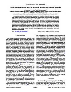
FIG. 1. (Color online) (a) Top and side views of geometric structures of 1T-PtSe2 monolayer. Gray and green atoms show Pt and Se atoms, respectively. (b) The phonon band diagram and (c) normalized Raman intensity of 1T-PtSe2 monolayer. (d) The electronic band diagram and (e) partial density of states of the monolayer structure. The Fermi level is set to zero. III.
MONOLAYER PtSe2
For a complete analysis how structural, electronic and phononic properties of the PtSe2 crystal evolve with the thickness, we first investigate characteristics of monolayers comprehensively. The optimized atomic structure of the octahedral coordination forming 1T polytype of PtSe2 belongs to P3m1 space group. As shown in Fig. 1(a), the Bravais lattice of 1T√ √ → − → x − yb), b = 0.5a( 3b x+ PtSe monolayer is hexagonal with lattice vectors, − a = 0.5a( 3b 2
−c = cb yb), → z . 1T-PtSe2 structure with D3d point group symmetry is composed of three
atomic sub-layers with Pt layer sandwiched between two Se layers. The lattice constant of the primitive unit cell of the monolayer 1T-PtSe2 structure is calculated to be 3.70 ˚ A which 4
TABLE I. The calculated parameters for the 1T-PtSe2 structures are; the lattice constants, a=b; overall thickness as the uppermost-lowermost Se-Se distance in the unitcell, h; the charge donation from Pt to Se atoms, ∆ρ; the cohesive energy per atom, ECoh ; Φ and µ are the values of work function and magnetization, respectively; Egap , the energy band gap of the structure. a=b
h
∆ρ ECoh
Φ
Egap
(˚ A) (˚ A/unitcell) (e− ) (eV) (eV) (eV) 1L PtSe2 3.70
2.68
0
4.43 5.36 1.17
2L PtSe2 3.73
7.39
0
4.53 4.64 0.19
3L PtSe2 3.74
12.04
0
4.57 4.67
0
4L PtSe2 3.75
16.67
0
4.59 4.67
0
Bulk PtSe2 3.77
2.56
0
4.65 0.79
0
is in perfect agreement with previously reported scanning transmission electron microscopy (STEM) data.46 The Pt-Se bond length in the 1T phase of PtSe2 crystal structure is found to be 2.52 ˚ A. Moreover, the thickness, defined as vertical distance between uppermost and lowermost Se layers, of 1T-PtSe2 monolayer is (2.68 ˚ A) is also close to the reported value of ˚.46 2.53 A It is also found that the monolayer 1T-PtSe2 is formed by a cohesive energy of 4.43 eV/atom which is comparable to the cohesive energy of MoSe2 and WSe2 (∼ 4.56 and ∼
5.15 eV/atom, respectively).47 According to Bader charge analysis, there is no net charge
transfer between bonded atoms in monolayer 1T-PtSe2 structure and the bond character is entirely covalent in monolayer 1T-PtSe2 structure. In addition, the work function is obtained as 5.36 eV in the monolayer 1T-PtSe2 which is higher than that of similar dichalcogenides such as MoSe2 and WSe2 (4.57 and 4.21 eV, respectively)48 . However, structures obtained from total energy optimization calculations may not correspond to the ground state structure, therefore; for a reliable analysis on the stability of a structure it is also necessary to examine the dynamical stability via phonon calculations. The phonon dispersion curves of the 1T-PtSe2 crystal structure are shown in Fig. 1(b). For the primitive unit cell of 1T-PtSe2 composed of 3 atoms, phonon spectrum includes 9 phonon, 3 acoustic and 6 optical, branches, Analysis of lattice dynamics shows that the decomposition of the vibration representation of optical modes at the Γ point is 5
1.3
2.5
1.28 1.26
2
1.24
1.5 Energy (eV)
CBM
1.22
3.75 Å 3.74 Å 3.73 Å 3.72 Å 3.71 Å
1 0.5 0
1.22 1.21 Eg (eV) = 1.20 1.19 1.18
CBM
VBM
1.2 1.18 0.01
VBM
0
-0.5 -1
-0.01
-1.5 K
M
Γ
-0.02
K
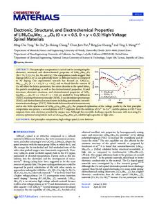
FIG. 2. (Color online) The SOC included electronic band diagrams of 1T-PtSe2 monolayer as a function of tensile biaxial strain. The Fermi level is set to zero. Side views show the valence band maximum (VBM) and conduction band minimum (CBM) on an enlarged scale.
Γ=2Eg +2Eu +A1g +A2u for the 1T-PtSe2 monolayer structure. Optical phonons include two doubly degenerate in-plane vibrational modes at 169 cm−1 (Eg ) and 218 cm−1 (Eu ), and two singly degenerate out-of-plane vibrational modes at 200 cm−1 (A1g ) and 223 cm−1 (A2u ). Vibrational spectrum with eigenfrequencies through whole the Brillouin Zone indicate that of the 1T-PtSe2 phase corresponds to a dynamically stable crystal structure. Regarding Raman intensities, in the vibrational spectrum of 1T-PtSe2 , there are two prominent peaks likely to be observed in experiments. As shown in Fig. 1(c), (i) one highly intense in-plane Eg mode at 169 cm−1 and (ii) one moderate intense out-of-plane A1g mode at 200 cm−1 . Due to strong covalent character between Pt and Se atoms, out-of-plane motion of the Se atoms has less contribution in the Raman intensity compared to in-plane motion of the Se atoms. Corresponding eigenvectors of the Raman active Eg and A1g modes are also sketched in Fig. 1(c). As shown in Fig. 1(d), (e), 1T-PtSe2 monolayer is an indirect band gap semiconductor with its valence band maximum (VBM) residing at Γ point and conduction band minimum (CBM) within Γ-M point. Calculations with, without spin-orbit interactions and HSE correction show that the band gaps of 1T-PtSe2 monolayer are 1.34, 1.17 and 1.66 eV, besides; no change is seen at the band edges of CBM and VBM. With the effect of spin-orbit coupling (SOC), double degenerate VBM is separated at Γ point about 0.4 eV in the 1T-PtSe2 6
monolayer and also CBM splits 170 meV at the point between Γ and M. It is seen that HSE correction increases the band gap about 0.5 eV. As seen in Fig. 1(e), PDOS shows that d and p orbitals of Pt, and p orbitals of Se are responsible for the VBM of the monolayer, whereas only d xy ,d yz ,d xz and d x2 −y2 orbitals (d pl ) of Pt are dominantly responsible for CBM of the 1T-PtSe2 structure. Since the effect of strain due the adjacent layers is inevitable in such lamellar crystal structures, before studying the thickness dependent properties, we investigate electronic and structural parameters under biaxial strain. Here we apply the strain by scanning the lattice parameters in between monolayer and bulk 1T-PtSe2 . It is found that the Pt-Se bond length monotonically increases, while tensile strain rate increases. As seen from Fig. 2, while VBM at the Γ point is quite insensitive against the biaxial strain, CBM at the Γ-M symmetry point shifts upwards slightly in the energy space. Hence, the reasonable tensile strain causes to change slightly the electronic band gap of the monolayer 1T-PtSe2 structure. Against tensile deformation, the 1T-PtSe2 monolayer is the quite robust semiconductor material which is the essential factor for its utilization in future nanoelectronics.
IV.
DIMENSIONAL CROSSOVER FROM MONOLAYER TO BULK
A.
Stacking Types and Thickness-Dependence of the Atomic Structure of 1T-
PtSe2
Stacking order of the sublayers in a layered material directly determines its structural, vibrational, electronic and optical properties. Therefore, theoretical prediction, prior to experimental synthesis, of stacking order is of importance. Possible stacking orders in 1T-PtSe2 crystal namely AA, AB, A’A, and A’B are presented in Fig. 3. It is found that energetically favorable stacking order is top to top (AA), as shown in Fig. 3 (a). In addition, AB, A’A, and A’B, stackings are found to be 159, 321 and 91 meV, respectively, less favorable than the ground state structure. The lattice constant of AA stacked structure, 3.73 ˚ A, is consistent with the experimentally reported value.28 Furthermore, the interlayer distances are calculated to be 2.14, 2.89, 3.61, and 2.63 ˚ A for AA, AB, A’A, and A’B stacking orders, respectively. A, with additional It is also seen that while the thickness of single layer PtSe2 is 2.68 ˚ 7
(a)
(b)
AA
AB
2.89 Å
2.14 Å
c a
GROUND STATE
(c)
∆E = 159 meV
(d)
AA
AB
3.61 Å
2.63 Å
∆E = 321 meV
∆E = 91 meV
FIG. 3. (Color online) Top and side views of crystal structure of bilayer 1T -PtSe2 ; (a) AA, (b) AB (c) A’A, and (d) A’B stacking orders. The ground-state energy differences are given under each stacking type labeled with △E.
layers thickness of each single layer is reduced and finally reaches to bulk value of 2.56 ˚ A. Moreover, going from bilayer to bulk, the interlayer distance (vertical vacuum spacing between the adjacent layers) also decreases from 2.14 to 2.07 ˚ A. Apparently, there is an increasing trend in layer-layer interaction in the out-of-plane direction and therefore, as a result of thickness-driven compression, covalent Pt-Se bonds are enlarged. As listed in Table I, lattice constant of the bilayer, trilayer, four-layer, and bulk structures are found to be 3.73, 3.74, 3.75, and 3.77 ˚ A, respectively.
B.
Thickness Dependence of Electronic Properties
In order to determine how the electronic characteristics are modified with increasing number of layers, we also calculate the electronic band dispersions of monolayer, bilayer, trilayer, and bulk PtSe2 . As shown in Fig. 4, going from monolayer to bilayer structure, the electronic band gap of the material rapidly decreases from 1.17 eV to 0.19 eV and it is also 8
3 Monolayer
Bilayer
Trilayer
Bulk
2
Energy (eV)
1 Pt(dpl)
Se(pz)
Se(px+py)
Se(pz)
0 Pt(dpl)
Pt(dpl)
Se(px+py)
Se(px+py)
Pt(dpl)
Se(px+py)
-1 Se(pz) -2
K
Γ
M
K
Γ
M
K
Γ
M
K
Γ
M
K
FIG. 4. (Color online) The electronic band dispersions of monolayer, bilayer, trilayer, bulk 1TPtSe2 . The Fermi level is set to zero.
found that PtSe2 crystals having thickness larger than the two layers all exhibit metallic behavior. In monolayer and bilayer structures of PtSe2 the CBM states are composed of d state electrons that occupy d xy ,d yz ,d xz and d x2 −y2 orbitals of Pt atom. While the location of CBM in BZ remains same (at the Γ-M) when going from monolayer to bilayer, VBM is shifted from the Γ to the K-Γ high symmetry point. It is also worth to note that local minimum energy state of the CBM of the monolayer within the K-Γ translocates its position in the Brillouin Zone to the K symmetry point with the effect of additional layers. Rapid decrease in band energy of CB states and increase in VB states leads to metallization starting from trilayers. On the other hand, the VBM state of the monolayer, that originates from px and py states of Se atoms, changes its energy space and takes position at the states energetically lower than the VBM state of the few-layer PtSe2 . Moreover, the VBM state of the bilayer, which consists of pz orbitals of Se atoms, crosses Fermi level and becomes one of the metallic transition band at the few-layer PtSe2 , as seen in the first case same trend appears in the pz orbitals of the Se atoms. It is obviously seen that the nesting in the corresponding state disappears while number of layer of PtSe2 increases. 9
C.
Thickness Dependence of Vibrational Properties
Investigation of the vibrational properties not only allows one to deduce the dynamical stability of the structure but also allows determination of characteristic properties such as bond strengths, layer thickness and polarizability. In this subsection, thickness dependency of phonon band dispersions, Raman intensities and eigen-frequency shifts of the prominent peaks of bilayer, trilayer, four layer and bulk PtSe2 are investigated. Figs. 5 (a)-(d) show the calculated phonon band structure of bilayer, trilayer, four layer and bulk PtSe2 . It is seen that all the phonon modes have real eigenfrequencies, which indicate that bulk and few-layered PtSe2 are stable. The appearance of small imaginary frequencies (less than 5 cm−1 ) near the gamma point are not an indication of instability, they are numerical artifacts caused by the inaccuracy of the FFT grid. As shown in Figs. 5 (a)-(d), while LA modes cross the low-frequency optical modes, highest-frequency dispersionless optical modes are well-separated from low-lying phonon branches. Computationally predicted modes at 152.2 and 212.5 cm−1 correspond to the Eg and A1g phonons of bulk PtSe2 are in good agreement with previous experimental results indicating the reliability of computational methodology of phonons.49 As shown in the figure, in addition to the Eg and A1g modes of the monolayer structure, additional peaks with low frequencies correspond to shear (S) and layer-breathing (LB) appear with the increasing thickness. It is found that S and LB modes are Raman active and as the number of layer increases from bilayer to bulk, the frequencies of S and LB modes increase from 38.8 and 44.0 cm−1 to 55.0 and 74.3 cm−1 , respectively. It is also worth noting that, as shown in Fig. 5 (e), Raman vibrational characteristics of the Eg phonon strongly depend on the material thickness. It appears that, with increasing thickness, layer-layer interaction originated compression on each sublayer yields two consequences in PtSe2 ; (i) phonon softening due to enlarged Pt-Se bonds and (ii) increasing Raman activity due to enhanced polarizability. It is also seen from Fig. 5 (f), when the number of layers is increased, A1g peak hardens while Eg peak softens. The downshift in the frequency of Eg peak is ascribed to the change in the dielectric screening environment for long-range Coulomb interactions as the thickness of the material increases. However, the upshift in the frequency of A1g peak is attributed to increasing interlayer interactions which enhance the restoring forces on the atoms.50,51 10
Frequency (cm-1)
250
(a)
200
(b)
150 100
LB
LB
50 S
S
Bilayer
Trilayer
0 Γ
M
K
Γ
Γ
M
K
Γ
Frequency (cm-1)
250
(c)
200 150 100
LB
LB
50
S
Four-Layer
S
0 Normalized Raman Intensity
(d)
Γ
M
Bulk
K
Γ
1.0
Γ
M
K
Γ
170 Bulk
Eg
220
(e)
(f) 165
0.5
215
Eg
A1g
160
210
Four-Layer Trilayer
0 150
155
Bilayer x10
160
Monolayer x1000
165
170
205
155 150 1L
2L
3L
4L
200 Bulk
FIG. 5. (Color online) The phonon band dispersions of (a) bilayer, (b) trilayer, (c) four-layer and (d) bulk. The S and LB mode frequencies are indicated. (e) Layer dependent Raman intensity of Eg mode. (f) Frequency shifts of the Eg and Ag modes with respect to number of layers. 1L, 2L, 3L and 4L denote monolayer, bilayer, trilayer and four-layer, respectively.
Therefore, the strong layer dependency of Raman intensity of Eg mode and peak positions of Eg and A1g modes can be used to determine the material thickness.
V.
CONCLUSIONS
In this study, we investigated thickness dependency of structural, vibrational and electronic properties of the 1T-PtSe2 by performing first-principles calculations. First, it was found that the monolayer of platinum diselenide forms a dynamically stable hexagonal 1T phase, and the monolayer is an indirect band gap semiconductor. The electronic nature of the monolayer structure changes negligibly under biaxial tensile deformation revealing the robust semiconductor character of the material. In addition, electronic dispersion calculations on crystals of various thickness showed that while monolayer and bilayer structures of 1T-PtSe2 are indirect band-gap semiconductors, all thicker 11
structures exhibit metallic character. The layer-dependent vibrational spectra of the 1T-PtSe2 structures reveal that Raman active shear mode, layer-breathing mode, Eg mode, and A1g mode display significant shifts indicating the increasing layer-layer interaction. Moreover, Raman intensity of the Eg phonon branch is found to be quite sensitive to the material thickness and therefore it can be used for determination of number of layers by Raman spectroscopy. Our study provides an insight into the electronic and vibrational properties of ultra-thin 1T-PtSe2 materials and also a computational strategy for identifying the number of layers of 1T-PtSe2 at the atomic scale.
VI.
ACKNOWLEDGMENTS
Computational resources were provided by TUBITAK ULAKBIM, High Performance and Grid Computing Center (TR-Grid e-Infrastructure). HS acknowledges financial support from the TUBITAK under the project number 117F095.
∗
[email protected]
1
B. C. Brodie, Philos. Trans. R. Soc. London 149, 249 (1859).
2
I. K. Schuller, Phys. Rev. Lett. 44, 1597 (1980).
3
K. S. Novoselov, A. K. Geim, S. V. Morozov, D. Jiang, Y. Zhang, S. V. Dubonos, I. V. Grigorieva, and A. A. Firsov, Science 306, 666 (2004).
4
A. K. Geim and I. V. Grigorieva, Nature 499, 419 (2013).
5
D. J. Late, B. Liu, J. Luo, A. Yan, H. S. S. Matte, M. Grayson, C. N. R. Rao, and V. P. Dravid, Adv. Mater. 24, 3549 (2012).
6
S. Joshi, F. Bischoff, R. Koitz, D. Ecija, K. Seufert, A. P. Seitsonen, J. Hutter, K. Diller, J. I. Urgel, H. Sachdev, J. V. Barth, and W. Auw¨ arter, ACS Nano 8, 430–442 (2013).
7
K. K. Kim, A. Hsu, X. Jia, S. M. Kim, Y. Shi, M. Hofmann, D. Nezich, J. F. Rodriguez-Nieva, M. Dresselhaus, T. Palacios, and J. Kong, Nano Lett. 12, 161 (2012).
8
H. L. Zhuang, and R. G. Hennig, Appl. Phys. Lett. 101, 153109 (2012).
12
9
P. Vogt, P. D. Padova, C. Quaresima, J. Avila, E. Frantzeskakis, M. C. Asensio, A. Resta, B. Ealet, and G. L. Lay, Phys. Rev. Lett. 108, 155501 (2012).
10
S. Cahangirov, M. Topsakal, E. Akt¨ urk, H. S¸ahin, and S. Ciraci, Phys. Rev. Lett. 102, 236804 (2009).
11
G. A. Parks, Chem. Rev. 65, 177 (1965).
12
A. I. Khan and D. O’Hare, J. Mater. Chem. 12, 3191 (2002).
13
B. Akbali, A. Yanilmaz, A. Tomak, S. Tongay, C. C ¸ elebi, and H. Sahin, Nanotechnology 28, 415706 (2017).
14
C. Ataca, H. S ¸ ahin, E. Akt¨ urk, and S. Ciraci, J. Phys. Chem. C 115, 3934 (2011).
15
M. Chhowalla, H. S. Shin, G. Eda, L. J. Li, K. P. Loh, and H. Zhang, Nat. Chem. 5, 263 (2013).
16
K. F. Mak, C. Lee, J. Hone, J. Shan, and T. F. Heinz, Phys. Rev. Lett. 105, 136805 (2010).
17
Y. Zhang, T. R. Chang, B. Zhou, Y. T. Cui, H. Yan, Z. Liu, F. Schmitt, J. Lee, R. Moore, Y. Chen, H. Lin, H. T. Jeng, S. K. Mo, Z. Hussain, A. Bansil, and Z. X. Shen, Nat. Nanotechnol. 9, 111 (2014).
18
A. Castellanos-Gomez, M. Poot, G. A. Steele, H. S. van der Zant, N. Agra¨ıt, and G. RubioBollinger, Adv. Mater. 24, 772 (2012).
19
Q. H. Wang, K. Kalantar-Zadeh, A. Kis, J. N. Coleman, and M. S. Strano, Nature Nanotech. 7, 699 (2012).
20
D. Jariwala, V. K. Sangwan, L. J. Lauhon, T. J. Marks, and M. C. Hersam, ACS Nano 8, 1102 (2014).
21
C. Tan and H Zhang, Chem. Soc. Rev. 44, 2713 (2015).
22
X. Qian, J. Liu, L. Fu, and J. Li, Science 24, 3549 (2014).
23
G. Y. Guo and W. Y. Liang, J. Phys. C: Solid State Phys. 19, 995 (1986).
24
G. Kliche, J. Solid State Chem. 56, 26 (1985).
25
J. S. L. Yeo, J. J. Vittal, W. Henderson, and T. A. Hor, J. Chem. Soc., Dalton Trans. 3, 328 (2002).
26
K. Ullah, S. Ye, S. B. Jo, L. Zhu, K. Y. Cho, and W. C. Oh, Ultrason. Sonochem. 21, 1849 (2014).
27
S. Ye and W. C. Oh, Mat. Sci. Semicond. Process. 48, 106 (2016).
28
Y. Wang, L. Li, W. Yao, S. Song, J. T. Sun, J. Pan, X. Ren, C. Li, E. Okunishi, Y.Q. Wang, E. Wang, Y. Shao, Y. Y. Zhang, H. T. Yang, E. F. Schwier, H. Iwasawa, K. Shimada, M.
13
Taniguchi, Z. Cheng, S. Zhou, S. Du, S. J. Pennycook, S. T. Pantelides, and H. J. Gao, Nano Lett. 15, 4013 (2015). 29
Y. Zhao, J. Qiao, P. Yu, Z. Hu, Z. Lin, S. P. Lau, Z. Liu, W. Ji, and Y. Chai, Adv. Mater. 28, 2399 (2016).
30
J. Du, P. Song, L. Fang, T. Wang, Z. Wei, J. Li, and C. Xia, Appl. Surf. Sci. 435, 476 (2018).
31
L. Li, W. Wang, Y. Chai, H. Li, M. Tian, and T. Zhai, Adv. Funct. Mater. 27, 1701011 (2017).
32
Y. Zhao, J. Qiao, Z. Yu, P. Yu, K. Xu, S. P. Lau, W. Zhou, Z. Liu, X. Wang, W. Ji, and Y. Chai, Adv. Mater. 29, 1604230 (2017).
33
X. Chia, A. Adriano, P. Lazar , Z. Sofer, J. Luxa, and M. Pumera, Adv. Funct. Mater. 29, 4306 (2016).
34
L. H. Zeng, S. H. Lin, Z. J. Li, Z. X. Zhang, T. F. Zhang, C. Xie, C. H. Mak, Y. Chai, S. P. Lau, L. B. Luo, and Y. H. Tsang, Adv. Funct. Mater. 1, 1705970 (2018).
35
Z. X. Zhang, L. H. Zeng, X. W. Tong, Y. Gao, C. Xie, Y. H. Tsang, L. B. Luo, and Y. C. Wu, J. Phys. Chem. Lett. 9, 1185 (2018).
36
S. Sattar and U. Schwingenschl¨ ogl, ACS Appl. Mater. Interfaces 9, 15809 (2017).
37
M. Sajjad, E. Montes, N. Singh, and U. Schwingenschl¨ ogl, Adv. Mater. Interfaces 4, 1600911 (2017).
38
W. Yao, E. Wang, H. Huang, K. Deng, M. Yan, K. Zhang, K. Miyamoto, T. Okuda, L. Li, Y. Wang, H. Gao, C. Liu, W. Duan, and S. Zhou, Nat. Commun. 8, 14216 (2017).
39
A. Ciarrocchi, A. Avsar, D. Ovchinnikov, and A. Kis, Nat. Commun. 9, 919 (2018).
40
G. Kresse and J. Hafner, Phys. Rev. B 47, 558 (1993).
41
G. Kresse and J. Furthm¨ uller, Phys. Rev. B 54, 11169 (1996).
42
J. P. Perdew, K. Burke, and M. Ernzerhof, Phys. Rev. Lett. 77, 3865 (1996).
43
S. Grimme, J. Comput. Chem. 27, 1787 (2006).
44
G. Henkelman, A. Arnaldsson, and H. Jonsson, Comput. Mater. Sci. 36, 354 (2006).
45
A. Togo, F. Oba, and I. Tanaka, Phys. Rev. B 78, 134106 (2008).
46
Y. Wang, L. Li, W. Yao, S. Song, J. T. Sun, J. Pan, X. Ren, C. Li, E. Okunishi, Y. Q. Wang, E. Wang, Y. Shao, Y. Y. Zhang, H. T. Yang, E. F. Schwier, H. Iwasawa, K. Shimada, M. Taniguchi, Z. Cheng, S. Zhou, S. Du, S. J. Pennycook, S. T. Pantelides, and H. J. Gao, Nano Lett. 15, 4013 (2015).
47
J. Lee, J. Huang, B. G. Sumpter, and M. Yoon, 2D Mater. 4, 021016 (2017).
14
48
C. Gong, H. Zhang, W. Wang, L. Colombo, R. M. Wallace, and K. Cho, Appl. Phys. Lett. 103, 053513 (2013).
49
M. O’Brien, N. McEvoy, C. Motta, J. Y. Zheng, N. C. Berner, J. Kotakoski, K. Elibol, T. J. Pennycook, J. C. Meyer, C. Yim, M. Abid, T. Hallam, J. F. Donegan, S. Sanvito, and G. S. Duesberg, 2D Mater. 3, 021004 (2016).
50
C. Lee, H. Yan, L. E. Brus, T. F. Heinz, J. Hone and S. Ryu, ACS Nano 4, 2695 (2010).
51
A. Molina-Sanchez and L. Wirtz, Phys. Rev. B 84, 155413 (2011).
15