www.nature.com/scientificreports
OPEN
Superconductivity Series in Transition Metal Dichalcogenides by Ionic Gating
received: 12 February 2015 accepted: 02 July 2015 Published: 03 August 2015
Wu Shi1, Jianting Ye1,2, Yijin Zhang1, Ryuji Suzuki1, Masaro Yoshida1, Jun Miyazaki1, Naoko Inoue1, Yu Saito1 & Yoshihiro Iwasa1,3 Functionalities of two-dimensional (2D) crystals based on semiconducting transition metal dichalcogenides (TMDs) have now stemmed from simple field effect transistors (FETs) to a variety of electronic and opto-valleytronic devices, and even to superconductivity. Among them, superconductivity is the least studied property in TMDs due to methodological difficulty accessing it in different TMD species. Here, we report the systematic study of superconductivity in MoSe2, MoTe2 and WS2 by ionic gating in different regimes. Electrostatic gating using ionic liquid was able to induce superconductivity in MoSe2 but not in MoTe2 because of inefficient electron accumulation limited by electronic band alignment. Alternative gating using KClO4/polyethylene glycol enabled a crossover from surface doping to bulk doping, which induced superconductivities in MoTe2 and WS2 electrochemically. These new varieties greatly enriched the TMD superconductor families and unveiled critical methodology to expand the capability of ionic gating to other materials.
Semiconducting transition metal dichalcogenides (TMDs) have attracted considerable interest as typical two-dimensional (2D) materials. Atomically flat and chemically stable thin layers of TMDs can be readily obtained via graphene-like mechanical exfoliation1 from bulk crystals due to the weak van der Waals interaction-based interlayer bonding2. By virtue of their semiconducting nature and defect-free crystal surfaces, thin exfoliated TMD layers are regarded to be ideal channel materials for field-effect transistors (FETs)3–5 and TMD-based FETs have been shown to possess remarkable electronic6,7 and opto-valleytronic properties8–13 as well as promising prospects for device applications14. Recent advances in the application of the field effect have been achieved using ionic gating by the formation of electrical double layers (EDLs); an EDL consists of narrow (~1 nm) spatial charge doublets that mimic a capacitor capable of accumulating an ultra-dense sheet of carriers (~1014 cm−2)15. EDL transistors (EDLTs) based on electrostatic ionic gating have proven to be a versatile tool for achieving novel device functionalities16,17 and inducing new electronic states18–21 at the interface between an ionic medium and a semiconductor channel. The use of EDLTs in TMD research has enabled the investigation of various interesting electronic properties, including ambipolar transport3,5, electric field control of spin polarization22, and circularly polarized electroluminescence12. High-density carriers have also bridged the gap to the quantum phases of TMDs through the field effect. The discovery of gate-induced superconductivity in MoS2 has revealed enhanced Tc and a dome-like phase diagram23; these features are absent in the chemically doped phase. In light of other available semiconducting TMDs and the effectiveness of electrostatic ionic gating, it is anticipated that this method may be applicable to induce superconductivity in other TMDs.
1
Quantum-Phase Electronics Center and Department of Applied Physics, The University of Tokyo, 7-3-1 Hongo, Bunkyo-ku, Tokyo, 113-8656, Japan. 2Zernike Institute for Advanced Materials, University of Groningen, The Netherlands. 3Center for Emergent Matter Science, RIKEN, Hirosawa 2-1, Wako 351-0198, Japan. Correspondence and requests for materials should be addressed to W.S. (email:
[email protected]) or Y.I. (email: iwasa@ ap.t.u-tokyo.ac.jp) Scientific Reports | 5:12534 | DOI: 10.1038/srep12534
1
www.nature.com/scientificreports/ Following the previous work on MoS25,23, here, we report a comprehensive study of transport properties and superconductivity in a semiconducting TMD series, specifically 2H-type MoSe2, MoTe2 and WS2. Transistor operation and carrier accumulation were significantly influenced by the interfacial energy level alignments of the different TMD materials at the same electrostatic ionic gating using an ionic liquid (IL: DEME-TFSI). Subsequently, the TMDs showed similar gate-induced insulator–metal transitions but did not all reach the superconducting states. In MoSe2, new gate-induced superconductivity (GIS) was found with a maximum Tc of 7.1 K that follows a dome-shaped phase diagram similar to that of MoS220,23. However, no superconductivity was observed in MoTe2 because of the low efficiency of electrostatic electron accumulation that could be achieved in this material using an IL. When the IL was replaced with a KClO4/PEG electrolyte, the electron doping could be significantly enhanced through a crossover to an electrochemical regime beyond the electrostatic limit. As a result, superconductivity in 2H-MoTe2 and WS2 were enabled with observed Tc values of approximately 2.8 K and 8.6 K, respectively. Thus, these results have revealed two series of superconductors in these TMDs. Additionally, this study established new strategies for ionic gating both for electrostatic charge accumulation and electrochemical carrier doping, thereby providing new capability for accessing a wide carrier concentration range and extending superconductivity in other material series.
Results
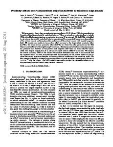
Evolution of electrostatic charge accumulation in MoX2 EDLTs. Figure 1a illustrates the crystal
structure of 2H-type transition metal dichalcogenides, MX2 (M = Mo or W; X = S, Se or Te), consisting of two-dimensional covalently bonded X− M− X layers. Due to their weak bonds formed through van der Waals interactions between the layers, thin flakes of MX2 can be readily isolated from bulk material via mechanical exfoliation and then fabricated into FET devices (see the Methods section). We used the EDLT structure and employed DEME-TFSI as a gate dielectric; the latter is a widely used IL that has been demonstrated to be capable of accumulating a high density of carriers at the interface even at low bias voltages15. Figure 1b presents a schematic diagram of the EDLT configuration and an optical image (bottom left) of a real MX2 device (MoSe2) prior to the application of the IL. A typical Hall bar geometry was adopted to measure the four-terminal resistance and the Hall carrier density. The thickness of the MoX2 flakes in this work ranged from approximately 20 nm to 100 nm as measured by atomic force microscopy (AFM). We confirmed that the 2H-type crystal structure was maintained in the thin flakes after transport measurements with IL gating as confirmed by synchrotron microbeam X-ray diffraction experiments (see Fig. S1 and Table S1 in the Supplementary Information). The gate voltage was applied through a droplet of IL under high vacuum and at a temperature just above the glass transition temperature of DEME-TFSI (i.e., 220 K) to suppress potential chemical reactions between the IL and the film surface5. Under these conditions, a TMD thin-flake EDLT can be modeled as a simple contact heterostructure between a semiconductor (i.e., the molybdenum-based TMD) and an electrolyte (i.e., the IL). Following the terminology used for electrolyte/semiconductor interface24–27, Fig. 1c,d present schematic energy-level diagrams before and after making the IL/TMD interface. Here, TMD refers specifically to a 2H-type MX2 with a finite band gap28,29. Even before applying a gate voltage, the electric double layer is formed and, in some cases, charge transfer across the interface (electrolysis) takes place until equilibrium is reached, i.e., the redox potential of the electrolyte (Eredox) aligns with the Fermi energy of the semiconductor (EF)24–27. The space charge layer in the semiconductor has an associated electric field represented by band bending. The work function ΦTMD influences the initial charge redistribution and the band bending at the interface before application of gate voltage. Because TMD work functions differ from each other30, the initial band bending varies among MoS2, MoSe2 and MoTe2 thin flakes for the same IL. Among these three dichalcogenides, MoTe2 exhibits the smallest work function, leading to the weakest initial band bending and the largest carrier injection barrier for electrons. Therefore, a systematic evolution of transistor performance with increasing threshold voltage is expected when the channel material is changed from MoS2 to MoTe2. By sweeping the gate voltages at a constant rate of 20 mV/s at 220 K, we measured the transfer curves for the different MoX2 (21 devices in total) that were all gated using DEME-TFSI. Figure 2a presents a comparison of the typical transfer curves of MoS2, MoSe2 and MoTe2 EDLTs measured with VDS = 0.1 V. All three MoX2 transistors displayed ambipolar behavior with systematic properties: within the same bias range, the two extremes of preferences for electron and hole accumulation were dominated by MoS2 and MoTe2, respectively, whereas MoSe2 exhibited a well-balanced ambipolar transistor performance that was most suitable for light-emitting devices31. The electron and hole conduction threshold voltages (as indicated by the black dashed lines in Fig. 2a) progressively shifted to higher voltages from MoS2 to MoTe2. The average values of the threshold voltage Vth versus the MoX2 work function (from ref. 30) are plotted in Fig. 2b, with each data point obtained by averaging 7 devices and the standard deviations shown by the error bars. The electron and hole conduction Vth values decreased with increasing MoX2 work function, consistent with the discussion of the interfacial energy-level alignment presented above. It is well known that in conventional FETs, Vth is largely governed by the contact effects (work function mismatch between the contact and the semiconductor) and by the deep trap states in the energy gap. However, it is noted that both of these factors take only minor roles in EDLTs5,32. First, the electrostatic screening (due to the ions close to the metal contact/semiconductor interface) in the liquid can further reduce the width of the Schottky barrier down to values comparable to the electrostatic screening Scientific Reports | 5:12534 | DOI: 10.1038/srep12534
2
www.nature.com/scientificreports/
Figure 1. Transition metal dichalcogenide (TMD) EDLT device and schematic diagrams of energylevel alignment at the IL/TMD interface. (a) Crystal structure of a 2H-type layered transition metal dichalcogenide MX2; M = Mo or W and X = S, Se, or Te. (b) EDLT device and measurement configuration. The bottom left shows an actual MoSe2 nanoflake device with a Hall bar geometry. This figure is drawn by W.S. (c) Schematic diagram of the energy levels of an independent ionic liquid and a TMD. (d) Schematic diagram of aligned energy levels at the IL/TMD interface. The initial band bending occurs when the IL touches the TMD surface. The vacuum level (VL), redox potential (Eredox), conduction band (Ec), valence band (Ev), Fermi energy (EF), and work function (ΦTMD) are defined and labeled in (c) and (d).
length in the ionic liquid (1–2 nm)5,32–34. Thus, tunneling-mediated carrier injection is more likely than thermal activation over a Schottky barrier. Second, because of the extremely large EDL capacitance CEDL (usually two orders of magnitude larger than the solid gate capacitance Csolid), the threshold voltage shift Δ Vth (=Ntrap/eCEDL) due to the filling of trap states (Ntrap) becomes negligible32. Because our devices were designed to access low-temperature quantum phases, it was critical to quantify the sheet carrier density n2D, which was therefore unambiguously determined through a Hall effect measurement. To eliminate any temporal change in n2D during ionic gating in MoX2 EDLTs, all Hall effect measurements were performed at temperatures below the freezing point of ion movement, where the total number of accumulated carriers is fixed. The Hall coefficient RH was found to change its sign as a function of the gate voltage VG and n2D = 1/|RHe| was linearly proportional to the gate bias VG in the electrostatic region (Fig. S2). The EDL capacitance can be derived through a linear fit to the n2D–VG plot. We focused on the electron side and compared the capacitances obtained from the n2D–VG plots for 15 different MoX2 devices, as shown in Fig. 2c. Even for the same MoX2 crystal and IL, the capacitance values were broadly distributed among the devices, possibly because of the existence of different surface states in the individual thin flakes after the fabrication process. However, MoTe2 clearly exhibited a smaller average capacitance value (4.1 μ F/cm2) than MoS2 (8.6 μ F/cm2) or MoSe2 (10.6 μ F/cm2), indicating that MoTe2 demonstrated the lowest efficiency in electron accumulation.
Superconductivity of MoSe2 by ionic liquid gating in an electrostatic regime. To verify that the electrostatic ionic gating method23 described above is applicable for inducing superconductivity in MoSe2 and MoTe2 thin flake EDLTs, we measured their transport properties down to 2 K by varying VG in the positive direction to access electron transport. The results are shown in the plot of the channel sheet resistance Rs versus T in Fig. S3 and the MoSe2 data are presented in Fig. 3a. All materials displayed clear insulator–metal transitions with increasing electron density under higher VG (Fig. S3). As shown in Fig. 3a, gate-induced superconductivity emerged in MoSe2 at VG = 2.4 V and developed further with further VG increase. However, no superconducting transition was observed in MoTe2 up to VG = 2.5 V (Fig. S3c), at which point a conductivity maximum was reached. At higher VG values, the carrier density Scientific Reports | 5:12534 | DOI: 10.1038/srep12534
3
www.nature.com/scientificreports/
Figure 2. Evolution of ambipolar transfer characteristics and electrostatic charge accumulation in MoX2 EDLTs. (a) Comparison of typical ambipolar transfer curves of MoS2, MoSe2 and MoTe2 EDLTs measured with VDS = 0.1 V at 220 K. VG was swept at a constant rate of 20 mV/s through the same IL, DEME-TFSI. The threshold voltages for the electron side (Vth_e) and the hole side (Vth_h) were determined by linearly extrapolating the IDS–VG curves to zero, as indicated by the black dashed lines. (b) Linear correlation between the threshold voltages and the work functions of MoX2. The threshold voltages are average values deduced from the transfer curves of 21 MoX2 devices with the same IL at 220 K. According to the black dashed lines, a semiconductor with a smaller work function exhibits larger or smaller threshold voltages for electron or hole accumulation, respectively. This can be explained by considering the energy-level alignment at the interface, as shown in Fig. 1d. (c) Capacitances for electron accumulation, Ce, deduced from sheet carrier density n2D–VG plots (Fig. S2b) for various MoX2 EDLT devices using the same IL, DEME-TFSI. Different symbols represent different devices, and the horizontal short dashed lines correspond to the average values. On average, MoTe2 exhibited the lowest EDL capacitance for electron accumulation.
was saturated (Fig. S6b) and the mobility decreased, precluding the formation of a more pronounced conducting state. The transport measurements were also conducted for all MoX2 devices via hole doping. Similar insulator–metal transitions also occurred as negative VG was applied (Fig. S4), but no hole superconductivity was observed down to 2 K for all MoX2. Further enhancement of hole density or decrease in temperature is required to achieve hole superconductivity. Now we consider the properties of the electron-doped superconductor. Figure 3b presents the temperature dependence of the normalized sheet resistance of the MoSe2 device at various VG (i.e., the device represented in Fig. 3a). It is evident that the superconducting transition can be controlled via electrostatic ionic gating. The Tc value increased with increasing VG, reaching a maximum of Tc = 7.1 K (defined as 90% of the total transition at VG = 3.2 V, where n2D = 1.69 × 1014 cm−2). This Tc value was higher than the maximum previously reported for Sr-doped MoSe2 (~5 K)35. Based on a precise determination of n2D using the Hall effect (Fig. S2), we show the relationship between Tc and n2D for the same MoSe2 device in Fig. 3c. In a similar manner to MoS2, the superconductivity in MoSe2 abruptly emerged above a critical carrier density n0. Subsequently, Tc increased with increasing n2D until a maximum was reached. This trend was also consistently observed in the Hc2 versus n2D phase diagram (Fig. S5). These similarities Scientific Reports | 5:12534 | DOI: 10.1038/srep12534
4
www.nature.com/scientificreports/
Figure 3. Superconductivity induced by electrostatic IL gating and phase diagram of electron-doped MoSe2. (a) Temperature dependence of the channel sheet resistance Rs at various liquid gate voltages for a MoSe2 EDLT device using DEME-TFSI as ionic media. (b) Normalized channel sheet resistance Rs/Rs (15 K) of the same MoSe2 EDLT device as a function of temperature for various liquid gate voltages from 2.4 V to 3.2 V. (c) Tc versus n2D phase diagram of electron-doped MoSe2. The MoS2 phase diagram (red shade) was taken from ref. 23 for comparison. Here, sheet carrier density n2D is obtained from Hall effect measurements and Tc is defined as the position corresponding to 90% of the total resistance drop. MoTe2 data are also presented in (c), showing no evidence of superconductivity down to 2 K (Tc = 0) because of the insufficient maximum carrier density achieved through electrostatic IL gating.
in the behaviors of MoS2 (red shade in Fig. 3c) and MoSe2 thus indicated that the dome-shaped phase diagram is a universal feature of gate-induced superconductivity in TMD systems. Figure 3c also shows n2D values for multiple MoTe2 devices (denoted by green symbols) with Tc = 0, indicating that no superconducting transitions were observed down to 2 K. We believe that the absence of superconductivity in MoTe2 may be due to the low maximum n2D of approximately 0.7 × 1014 cm−2, which is much smaller than the accumulation on MoS2 or MoSe2. This difference can be attributed to the fact that MoTe2 demonstrated the largest threshold voltage Vth (bottom panel of Fig. 2a) and the smallest capacitance Ce (Fig. 2c) during transistor operation in the electrostatic region.
Superconductivity of MoTe2 by electrolyte gating in an intermediate doping regime. To induce superconductivity in MoTe2, it is necessary to enhance the carrier density through more efficient transistor operation. The threshold voltage can be reduced by choosing ILs with smaller work functions. However, this achieved only a moderate enhancement in the carrier density because of the slight increase in capacitance and a significant n2D saturation observed with increasing VG (Fig. S6). We then found that the limitations on carrier accumulation could be surmounted by replacing the organic IL with the KClO4/PEG electrolyte. Figure 4a compares the channel current values IDS for MoTe2 devices fabricated using the two ionic media: the IL (DEME-TFSI) and the KClO4/PEG electrolyte. For IL gating, an increase in IDS was initiated at a large threshold voltage of approximately 1 V and was no longer observed when VG exceeded 2.5 V, indicating a limit on the formation of a more conductive channel. This peak behavior of IDS versus VG was associated with n2D saturation and was confirmed in multiple devices, implying that the observed behavior was not related to device degradation. For KClO4/PEG electrolyte gating, electrostatic electron accumulation occurred at a much smaller threshold voltage and induced a rapid increase of IDS, reaching a high conducting state at VG approximately 3.5 V. The conducting state was then sustained as VG was continuously increased up to 6 V. This gave rise to the observation of good metallic conduction followed by a superconducting transition at low temperatures, as shown in Fig. 4b. Scientific Reports | 5:12534 | DOI: 10.1038/srep12534
5
www.nature.com/scientificreports/ The magnetic field dependence of the Rs− T curves (Fig. 4c) further confirmed the existence of superconductivity at Tc = 2.8 K (defined as the temperature corresponding to 90% of the normal-state resistance at H = 1 T). Since superconductivity in MoTe2 has never been reported, the result in Fig. 4 marks the discovery of a new superconductor in the 2H-MoX2 family. Limited by the much lower ionic mobility in an electrolyte compared with an IL, we applied a VG at 300 K for the KClO4/PEG electrolyte; at this temperature, the ions were sufficiently mobile. At such a high temperature, an increase in the leakage current associated with the saturation of IDS was observed above VG = 3.5 V (as shown in the inset of Fig. 4a), indicating that electrolysis of PEG or potassium intercalation may have occurred. At 20 K, n2D reached 0.9 × 1014 cm−2, only slightly higher than the maximum observed for IL gating. We define this voltage range for nearly saturated IDS as an intermediate regime beyond the electrostatic limit as it could be followed by an electrochemical regime at a higher VG where potassium intercalation may occur more effectively into the entire flake and eventually become dominant.
Superconductivity of WS2 by electrolyte gating in an electrochemical regime. WS2 is another member of semiconducting TMDs, where bulk superconductivity was known to occur at 3.5 K by conventional chemical doping of Sr35. Recently, ionic gating using IL was found to induce superconductivity at 4 K36. To confirm the different doping mechanism using the KClO4/PEG electrolyte as ionic media and gain access deeper into the electrochemical regime in WS2, we further increased our voltage bias up to 12 V and systematically studied the evolution of carrier accumulation in a WS2 device labeled as A. Figure 5a presents the channel current values IDS as a function of VG measured at 300 K (see the complete data in Fig. S7). We can see that IDS went through the similar electrostatic and intermediate doping regimes reaching a limited value similar to that of MoTe2 described above; however, here, the limited IDS (approximately 17 μ A at VG = 6 V) corresponded to a metallic state that failed to access the superconducting region. This limit was clearly broken when VG exceeded approximately 7 V, where a second rapid upturn of IDS strongly indicated an effective electrochemical doping process, i.e., ion intercalation under high bias. This was supported by the distinctive large hysteresis (magenta dashed line in Fig. 5a) manifesting the intercalation and de-intercalation in a VG scan cycle. Because the device nearly recovered its pristine state after VG was restored back to zero, the low temperature transport can be measured after the in situ change of VG in a similar way as for the measurements in the electrostatic regime using ionic liquids. As shown in Fig. 5a, we also measured the carrier density nHall by the Hall effect at 200 K (also see Fig. S8). Here, nHall corresponds to the sheet carrier density n2D in the electrostatic regime, whereas beyond the electrostatic regime, nHall corresponds to the projected carrier density, which is essentially the bulk density n3D multiplied by the thickness of the doped sample. Examination of the n2D values (as shown in Fig. 5a) measured by the Hall effect at 200 K (denoted by circle symbols) showed that in the intermediate region, nHall increased very slowly until reaching an upper limit VG of approximately 7 V; this is followed by a rapid nHall increase reaching nHall = 4.7 × 1015 cm−2 at VG = 12 V, more than one order of magnitude higher than the maximum value obtained in the electrostatic region. Accordingly, the capacitance deduced from the nHall–VG data in the electrochemical region was much higher, achieving up to 200 μ F/cm2, providing strong evidence that the carrier doping reaches far beyond the level achieved in the electrostatic regime. We then focused on the transport properties of the electrochemically doped WS2. Figure 5b presents the results for RS as a function of temperature on the log scale for device A at various VG from 6 V to 12 V. We observed good metallic conduction followed by a superconducting transition at the same onset transition temperature (the dashed vertical line in Fig. 5b) for VG at 9 V, 10 V and 12 V. The transition can be completely destroyed by applying a magnetic field of 2 T as indicated by the dashed curves in Fig. 5b, providing strong evidence of superconductivity. Unlike the gate modulation of Tc observed in IL-gated MoSe2 (Fig. 3b), here, the onset Tc value did not change with VG. One possible explanation is that the superconducting phase is a line-phase compound in terms of K concentration. Potassium ions started to intercalate between the WS2 layers when VG exceeded a critical value (~7 V for device A). Then, a particular KxWS2 line-phase compound that exhibited a superconducting transition with a fixed Tc was formed at approximately 9 V. In this initial state where superconductivity appeared, the sample consists of a mixture of nonsuperconducting phase with lower x and the superconducting phase. As VG further increased, the superconducting phase gradually grew and finally occupied a substantial portion of the whole channel, reaching the “zero resistance” state (Rs