PHYSICAL REVIEW B 78, 245402 共2008兲
Superlattice structures of graphene-based armchair nanoribbons H. Sevinçli,1 M. Topsakal,2 and S. Ciraci1,2,* 1Department
of Physics, Bilkent University, Ankara 06800, Turkey of Materials Science and Nanotechnology, Bilkent University, Ankara 06800, Turkey 共Received 27 July 2008; revised manuscript received 27 October 2008; published 1 December 2008兲
2UNAM-Institute
Based on first-principles calculations we predict that periodically repeated junctions of armchair graphene nanoribbons of different widths form multiple quantum well structures. In these superlattice heterostructures the width as well as the energy-band gap is modulated in real space and specific states are confined in certain segments. Not only the size modulation, but also composition modulation, such as periodically repeated and commensurate heterojunctions of boron nitride and graphene honeycomb nanoribbons, results in a multiple quantum well structure. The geometrical features of the constituent nanoribbons, namely, their widths and lengths, the form of the junction, as well as the symmetry of the resulting superlattice, are the structural parameters available to engineer electronic properties of these quantum structures. We present our analysis regarding the variation of the band gaps and the confined states with these structural parameters. Calculation of transmission coefficient through a double barrier resonant tunneling device formed from a finite segment of such a multiple quantum well structure and placed between metallic electrodes yields resonant peaks which can be identified with electronic states confined in the well. We show that these graphene-based quantum structures can introduce interesting concepts to design nanodevices. Relevance of the quantum structures are discussed in view of the most recent experimental results. DOI: 10.1103/PhysRevB.78.245402
PACS number共s兲: 73.22.⫺f, 72.80.Rj, 75.70.Ak
I. INTRODUCTION
Superlattices and various quantum structures obtained thereof have been the subject of active research in the past two decades. Commensurate or pseudomorphic junctions of two different semiconductors have been grown layer by layer to form a periodically repeating superlattice structure with sharp lattice-matched interface.1–3 Owing to the band discontinuities at the interface, they behave as a multiple quantum well structure according to the effective mass theory. Electrons confined in these quantum wells exhibit twodimensional 共2D兲 electron-gas behavior with interesting quantum effects.4 Two-dimensional conduction-band electrons 共valence-band holes兲 confined to the wells have displayed a number of electronic and optical properties.1–6 Formation of quantum structures in one dimensional 共1D兲 systems have also been considered. For example, 1D multiple quantum wells or a series of quantum dots have been shown to form on a semiconducting zigzag nanotube by applying modulating radial strain and hence by forming bandgap modulation in real space.7,8 Multiple quantum wells are also obtained by the periodic junction of bare and hydrogenated zigzag carbon nanotubes.9 Similar quantum structures and confinement have been shown to occur in the junction of 共BN兲nCn linear chains.10 Recent advances in materials growth and control techniques have made the synthesis of the isolated 2D honeycomb crystal of graphene possible.11–13 Owing to its unusual electronic energy-band structure leading to the charge carriers resembling massless Dirac Fermions, graphene introduced new concepts and initiated active research.14–18 For example, quasi-1D graphene nanoribbons 共GNRs兲 exhibit interesting size- and geometry-dependent electronic and magnetic properties.19–23 Also graphene nanoribbons less than 10 nm wide with ultrasmooth edges have already been produced.24 In the same work, a graphene structure having three segments of graphene nanoribbon with different widths 1098-0121/2008/78共24兲/245402共8兲
has been obtained. This can be viewed as a finite segment of a graphene nanoribbon superlattice. Moreover, patterning of graphene nanoribbons13 and also graphene nanoribbons with varying widths17,25 has been achieved experimentally. With these developments the quantum well structures in graphenebased nanoribbons have been a subject of interest. In this work, based on first-principles, as well as empirical tight-binding 共ETB兲 calculations we show that periodically repeating heterojunctions made of armchair graphene nanoribbons of different widths can form stable superlattice structures. These superlattices are unique, since both their width and energy-band gap are modulated in real space. As a consequence, in addition to the propagating states, specific states are confined in certain regions. Confinement increases and turns to a complete localization when the lengths of the nanoribbon segments with different widths increase. This situation can be viewed as a series of quantum dots. Widths, lengths, chirality of constituent nanoribbons, and the symmetry of the junction can be varied to engineer these quantum structures with interesting electronic and transport properties. Further to these superlattices based on the width-modulated graphene armchair nanoribbons, we also show that multiple quantum well structures can be formed via composition modulation of commensurate heterojunction of boron nitride 共BN兲 and graphene armchair nanoribbons of the same width. These quantum structures are of particular interest, since they show effects analogous to those of 2D semiconductor superlattices. Finally, our transport calculations demonstrate that specific finite-size quantum structures can operate as resonant tunneling double barriers 共RTDB兲 with resonances—characteristics of confined quantum well states. In view of the recent experimental studies,13,17,24,25 present results related with graphene-based nanoribbons and their heterojunctions of diverse geometry can, in fact, be a candidate for a class of nanodevices with a richness of transport properties.
245402-1
©2008 The American Physical Society
PHYSICAL REVIEW B 78, 245402 共2008兲
SEVINÇLI, TOPSAKAL, AND CIRACI
Optimized atomic geometry of superlattices and corresponding electronic structure are obtained by performing first-principles plane-wave calculations26,27 within densityfunctional theory 共DFT兲 共Refs. 28 and 29兲 using projector augmented wave 共PAW兲 potentials.30 The exchangecorrelation potential is approximated by generalized gradient approximation 共GGA兲 using PW91 functional31 both for spin-polarized and spin-unpolarized cases. All structures are treated within supercell geometry using periodic boundary conditions. A plane-wave basis set with kinetic-energy cutoff of 500 eV is used for graphene as well as for BN. In the self-consistent potential and total-energy calculations the Brillouin zone 共BZ兲 is sampled by 共1 ⫻ 1 ⫻ 35兲 special k points for nanoribbons. This sampling is scaled according to the size of superlattices. All atomic positions and lattice constants are optimized by using the conjugate gradient method where total energy and atomic forces are minimized. The convergence for energy is chosen as 10−5 eV between two steps, and the maximum force allowed on each atom is 0.02 eV/ Å. The superlattices having large width and hence unit cells with very large number of atoms are treated by using ETB calculations. The tight-binding Hamiltonian has the simple form HETB = −t兺具i,j典共a†i b j + H.c.兲, where a†i 共b†j 兲 creates an electron on site Ri 共R j兲 of the A 共B兲 sublattice of the bipartite graphene lattice and ai 共b j兲 are the corresponding annihilation operators. The nearest-neighbor 共具i , j典兲 hopping energy is t ⯝ 2.7 eV 共Ref. 32兲. In the transport calculations, we use nonequilibrium Green’s function 共NEGF兲 formalism33 implemented together with DFT 共details of the NEGF+ DFT method can be found in Ref. 34兲. As a requirement of the partitioning scheme we employ, a localizedorbital basis set 共double plus polarization numerical orbitals兲 is used in place of the plane-wave basis set. The results obtained from plane-wave and local-orbital DFT calculations are verified to yield consistent results. We further optimize the atomic structure before transport calculations. In transport calculations the exchange-correlation potential is approximated by GGA with PBE functional.35 During the selfconsistent calculation 21 special k points are used and the maximum energy difference is set to 10−4 eV as the convergence criteria. In order to check the consistency of the different methods used, we compare the electronic band structures obtained from these calculations for AGNR共26兲 in Fig. 1.
FIG. 1. 共Color online兲 Band structure of AGNR共26兲 calculated with the three different methods used in this work: 共a兲 plane-wave DFT, 共b兲 localized-orbital DFT, 共c兲 and ETB.
As an example, we present the electronic structure and charge density of AGNR共10兲 and AGNR共14兲 nanoribbons in Figs. 2共a兲 and 2共b兲. The band-gap values of bare AGNR共10兲 and AGNR共14兲 are calculated to be 0.44 and 1.10 eV, respectively. According to isosurface plots one distinguishes the relatively uniform states 共having their charge uniformly distributed across the nanoribbon兲 from the edge states 共having their charge accumulated at both edges of the ribbon兲. Owing to the interaction between two edges of the narrow ribbon, the bands of edge states split. Upon termination of the carbon dangling bonds by atomic hydrogen, the edge states of AGNR共10兲 and AGNR共14兲 disappear and their energy-band gaps change to 0.39 and 1.57 eV, respectively. Since hydrogen-terminated AGNRs are stable at ambient conditions, in the rest of the paper we consider their superlattices unless stated otherwise. We note that defect-free bare and hydrogen-terminated armchair graphene nanoribbons have nonmagnetic ground
II. ARMCHAIR NANORIBBONS
The electronic structure and the magnetic properties of GNRs are primarily determined by their edge shapes and widths.19–23 We first consider the bare and hydrogenterminated armchair graphene nanoribbons AGNR共n兲; n being the number of carbon atoms in the primitive unit cell. All AGNR共n兲 are semiconductors and their band gaps Eg vary with n. We find that the band gap is small for n = 6m − 2 共m being an integer兲, but from n = 6m to n = 6m + 2 it increases and passing through a maximum it becomes again small at the next minimum corresponding to n = 6m + 4. As Eg oscillates with n its value decreases eventually to zero as n → ⬁. The results are in good agreement with the earlier works.23
FIG. 2. 共Color online兲 共a兲 Bare and hydrogen-terminated AGNR共10兲. Atomic geometry, electronic band structure, and isosurface charge densities of edge and “uniform” states. The primitive unit cell is delineated with dashed lines and includes n = 10 carbon atoms. Carbon and hydrogen atoms are shown by large and small balls. 共b兲 Same for AGNR共14兲. All data in this figure are calculated by first-principles method 共Refs. 26 and 27兲.
245402-2
PHYSICAL REVIEW B 78, 245402 共2008兲
SUPERLATTICE STRUCTURES OF GRAPHENE-BASED…
FIG. 3. 共Color online兲 共a兲 Possible junction angles leading to armchair or zigzag edge shapes. 60° angle with the longitudinal axis results in armchair edge at the interface, whereas 30° and 90° give zigzag edges. Some of the possible superlattice shapes are shown; namely, 共b兲 sharp rectangular, 共c兲 smooth, 共d兲 and sawtoothlike.
state. Recently it has been shown that 3d-transition-metal atoms adsorbed to armchair nanoribbons induce permanent magnetic moment and hence give rise to interesting magnetic properties.36 Similarly, specific vacancy defects in AGNR can induce permanent magnetic moments.37 On the other hand, bare and hydrogen-terminated zigzag graphene nanoribbons 共ZGNRs兲 have spin polarized edge states.20 The edge states having a high density of states near the Fermi energy give rise to a magnetic transition. Eventually ZGNR has edge magnetism with opposite spins populated at opposite edges. Here we consider only the superlattice structures made by armchair nanoribbons; the superlattice structures of zigzag nanoribbons are not discussed in this paper. In a short letter we showed that the spins can be confined in quantum structures formed from the zigzag ribbons.38 III. SUPERLATTICE STRUCTURES A. Graphene superlattices
The remarkable properties of GNRs discussed above, especially their band gap rapidly varying with their widths, suggest that the heterostructures formed by the segments of AGNRs with different n 共or width兲 may have interesting functions. Here the crucial issues to be addressed are how the electronic structure will be affected from the discontinuity of crystal potential at the junction, what the character of the band discontinuity and the resulting band alignment will be, and whether these discontinuities will result in confined states. Relative to the longitudinal axis in an armchair direction one can distinguish three possible angles to make junctions with armchair or zigzag edge shapes as shown in Fig. 3共a兲. A 60° angle gives rise to the armchair edge at the interface, whereas 30° and 90° angles result in zigzag edges. Some of the possible superlattice shapes are given in Figs. 3共b兲–3共d兲.
FIG. 4. 共Color online兲 共a兲 Atomic structure of AGSL共n1 = 10, n2 = 14; s1 = 3, s2 = 3兲. The superlattice unit cell and primitive unit cell of each segment are delineated. 共b兲 Band structure with flat bands corresponding to confined states. 共c兲 Isosurface charge density of propagating and confined states. 共d兲 Variation of various superlattice gaps with s1 = s2. 共e兲 Confinement of states versus s1 = s2 calculated by ETB. All data except those in 共e兲 are calculated by using first-principles method 共Refs. 26 and 27兲.
To avoid mixed edge shapes we focus on the junctions with smooth interfaces making 60° angle with the longitudinal axis. To this end we first consider a superlattice AGSL共n1 , n2 ; s1 , s2兲 made by the segments of AGNR共n1兲 and AGNR共n2兲. Here, s1 and s2 specify lengths 共in terms of the number of unit cell兲 of the segments having different widths. Figure 4 shows the superlattice AGSL共10,14;3,3兲. This superlattice is formed by periodically repeating the heterojunction of the segments of AGNR共10兲 and AGNR共14兲; each segment having three unit cells. The same superlattice can be visualized by periodically deleting one row of carbon atoms at both edges of AGNR共14兲 to form periodic AGNR共10兲/ AGNR共14兲 junction. Upon junction formation, dramatic changes occur in the band structure of this superlattice. While highest 共lowest兲 valance 共conduction兲 band is dispersive and their states propagate across the superlattice, the second valence and conduction bands are flat and their states are confined to the wider part of AGSL共10,14;3,3兲 consisting of a segment of AGNR共14兲. These latter flat-band states are identified as confined states. Similar quantum-dot structures with sharp peaks in the density of states have also been revealed on the Z-shaped nanoribbons.39 The superlattice AGSL共10,14;3,3兲 in Fig. 4共a兲 can be viewed as a thin slab with periodically modulated width in
245402-3
PHYSICAL REVIEW B 78, 245402 共2008兲
SEVINÇLI, TOPSAKAL, AND CIRACI
the xy plane. The electronic potential in this slab is lower 共V ⬍ 0兲 than outside vacuum 共V = 0兲. Normally, electrons in this thin slab propagate along the x axis. Some electronic states in the wide segment are reflected from the discontinuities at the junction and eventually become confined. In these GNR superlattices the atomic arrangement and lattice constants at both sides of the junction are identical; the heterocharacter concerns only the different widths of the adjacent segments at different sides. According to this simple picture, the larger ⌬n = n2 − n1, the stronger becomes the confinement. As justified in further discussions, these arguments are relevant for superlattices with long constituent segments. Note that AGNRs can be constructed by using two different unit cells 共i.e., those consisting of complete hexagons or incomplete hexagons兲 reproducing the same crystal structure when translational symmetry is imposed 关see the AGNR unit cells in Fig. 4共a兲兴. For the wider parts of the superlattice the one with complete hexagons is preferred in order to avoid having carbon atoms with coordination number 1 at the interfaces. For AGSL superlattices with reflection symmetry the narrow region is made by unit cells having complete or incomplete hexagons depending on whether 共n2 − n1兲 / 4 is an even or odd number, respectively. In addition to n1, n2, s1, s2, the symmetry of the junction, ⌬n = n2 − n1, even-odd disparity of n1 / 2 and n2 / 2, the type of the interface between two different ribbons, and the overall shape of the superlattice 共namely, sharp rectangular, smooth wavy, or sawtoothlike兲 influence the electronic properties. We define the confinement as the weight of the wave function in the segment it becomes confined, say, s2, i.e., 兰s2兩⌿共r兲兩2dr, and examine the variation of specific band gaps and confinement of states with the size of the segments and supercell. For example, as shown in Fig. 4共d兲, as s1 = s2 increases, various superlattice band gaps decrease, but the confinement of specific states increases. This is a clear evidence for quantum size effect. The role of s1 and s2 is, however, different in the confinement of a state. For example, for ⌿1共r兲 the effect of barrier is complete already for s1 ⱖ s2, and the confinement of the state does not change considerably when s2 is fixed but s1 is increased. On the other hand, the confinement of this state increases when s1 is fixed, but s2 increased. Other confined states display similar behavior. It appears that as a consequence of quantum size effect the energy of ⌿1共r兲 decreases as the size s2 of the well increases. Less kinetic energy of the confined electron 共i.e., hence higher barrier height兲 causes suppression of the penetration into the barrier region. When s2 is kept fixed, the energy of the confined electron also remains the same. The exponential decay rate of the tail is unchanged under the barrier region, only the length of the tail changes with s1. Consequently, the strength of confinement is less sensitive to s1 once the electron is confined to the s2 region. The rate of change of band gaps with strain ⑀ = ⌬c / c 共⌬c being the change of lattice constant under uniaxial stress along the x axis.兲 of nanoribbon superlattice structures is also a notable feature, which may be interesting for future straingauge device applications. In Figs. 5共a兲 and 5共b兲 we present our results for the variation of Eg and other relevant gaps of the nanoribbon superlattice AGSL共10,14;3,3兲 and also its constituent AGNRs for the sake of comparison. Strong de-
FIG. 5. 共Color online兲 共a兲 Variation of band gaps Eg, ⌬1, and ⌬2 of the nanoribbon superlattice AGSL共10,14:3,3兲. 共b兲 Variation of the total energy ET with respect to ⑀ and the force constant SL 关in eV/ Å兴 for AGSL共10,14;3,3兲 and its constituent nanoribbons. All data in this figure are calculated by using first-principles method 共Refs. 26 and 27兲.
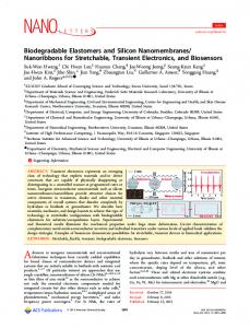
pendence on ⑀ is impressive. That these superlattice structures are quasi-1D stiff materials is shown by the variations of their total energies ET with respect to ⑀ in Fig. 5共b兲. The force constant of the superlattice calculated by SL = 2ET / c2 is in good agreement with the equivalent force constant eq,SL = 共s1 / n1 + s2 / n2兲−1 calculated in terms of the force constants of the constituent nanoribbons n1 and n2. This shows that elastic properties of superlattices comply with Hooke’s law for small ⌬n = n2 − n1. Deviations of s1 from s2 causes Eg and the band structure to change 共see Fig. 6兲. For example, AGSL共10, 14; s1 , s2兲 has Eg = 0.66, 0.48, 0.38, 0.32, 0.27, 0.22 eV for s2 = 3, but s1 = 3 , 4 , 5 , 6 , 7 , 8, respectively. Conversely, Eg = 0.66, 0.72, 079, 0.83, 0.84, 0.86 eV for s1 = 3, but s2 = 3 , 4 , 5 , 6 , 7 , 8, respectively. On the other hand, the energy of the flat-band states ⌬1 confined to s2 and their weight are practically independent of s1. Variation of ⌬n = n1 − n2 results in a wide variety of electronic structures. For example, in contrast to AGSL共10,14;3,3兲 the highest valence and lowest conduction bands of AGSL共10,18;3,3兲 are flat bands with Eg = 0.70 eV; dispersive bands occur as second valence and conduction bands having a gap of 1.19 eV between them 共see Fig. 7兲. Here ⌬2 = 1.18, 0.86, 0.66, 0.51, 0.43, 0.35 eV with s2 = 3 but s1 = 3 , 4 , 5 , 6 , 7 , 8, respectively, whereas ⌬1 remains unaltered 共⌬1 ⬇ 0.70 eV兲. The situation is even more complex for AGSL共10,22;3,3兲. While the first and the second bands are dispersive in both valence and conduction bands with a direct band gap 0.23 eV, flat bands occur as third bands with a gap of 2.61 eV between them. The states associated with the flat bands near the Fermi level are confined at the wider part of the superlattice. It should be noted that the band gap of nanoribbons Eg is underestimated by the DFT calculations.40 Since we consider structures which have already a band gap, its actual value does not affect our discussion qualitatively, but an enhancement of predicted properties 共such as the strength of confinement兲 can be expected.
245402-4
PHYSICAL REVIEW B 78, 245402 共2008兲
SUPERLATTICE STRUCTURES OF GRAPHENE-BASED…
(a) AGSL(10,14;3,3)
AGSL(10,14;8,3)
(b) AGSL 3
(10,14;3,3)
3
AGSL (10,14;4,3)
3
AGSL (10,14;5,3)
3
AGSL (10,14;6,3)
3
AGSL (10,14;7,3)
3
2
2
2
2
2
1
1
1
1
1
1
0
0
0
0
0
-1
-1
-1
-1
-1
-1
-2
-2
-2
-2
-2
-2
Energy (eV)
2
0
Eg ∆ 1 ∆ 2
-3 Γ
kx
X
-3 Γ
kx
X
-3
Γ
kx
X
-3
Γ
kx
X
-3
Γ
kx
X
-3
AGSL (10,14;8,3)
Γ
kx
X
(c) Eg
0.66 eV
0.48 eV
0.38 eV
0.32eV
0.27 eV
0.22 eV
∆1
2.03 eV
2.05 eV
2.05 eV
2.05 eV
2.05 eV
2.05 eV
∆2
2.26 eV
1.92 eV
1.66 eV
1.47eV
1.30 eV
1.16 eV
FIG. 6. 共Color online兲 The effect of the variation of narrower region s1 of AGSL 共10, 14; s1 , 3兲 from s1 = 3 to 8. 共a兲 Atomic structure and superlattice unit cell. 共b兲 The variation of band structures. 共c兲 The numerical values for energy gaps Eg, ⌬1, and ⌬2. Eg is the actual band gap of the structure which comes from a dispersive state. ⌬1 is the band gap of highest localized state while ⌬2 is the band gap for the next dispersive state. The energy of the flat-band states related with ⌬1 are confined to s2 and their weights are practically independent of s1. All data in this figure are calculated by using first-principles method 共Refs. 26 and 27兲.
Moreover in Fig. 8 we demonstrate that the confined states can occur not only in narrow 共small n1 and n2兲, but also in wide superlattices having significant modulation of the width. The above trends corresponding to small n1 and n2 become even more interesting when n1 and n2 increase. The electronic band structure of AGSL共n1 , n2 ; s1 , s2兲 with n1 = 42 or 82, but n2 ⬎ n1 and s1 = s2 ⱖ 3 calculated using ETB method shows that for small ⌬n, confinement is weak and bands are dispersive, but confinement increases as ⌬n increases. Interestingly, Eg of AGSL共n1 = 42, n2 ; 3 , 3兲 is, respectively, 0.46, 0.12, 0.49, and 0.04 eV for n2 = 46, 50, 54, and 58. In ETB method used here, the Bloch states having band index l and wave vector k are expressed in terms of the linear combination of the orthonormalized Bloch sums i共k , r兲 constructed for each atomic orbital pz localized at different carbon atoms, i, with the proper phase of k, namely,
FIG. 7. 共Color online兲 共a兲 Band structure of AGSL共10,18;3,3兲 with flat bands corresponding to confined states 共⌬1 = Eg兲. 共b兲 Isosurface charge density of propagating and confined states. 共c兲 Density of states 共DOS兲 of AGSL共10,18;3,3兲 with sharp peaks corresponding to confined states. Calculations are performed by using first-principles method 共Refs. 26 and 27兲.
l共k , r兲 = 兺iai,l共k兲i共k , r兲. Accordingly, the contribution of the orbital at site i to the normalized charge density of l共k , r兲 is given by i = 兺l兩ai,l共k兲兩2. In Fig. 8, i is scaled with the radius of circles located at atomic site i. Electronic structure is also strongly dependent on whether the geometry of the superlattice is symmetric 共having a reflection symmetry with respect to the superlattice axis along the x direction兲 or saddle 共one side is straight, other side is periodically carved兲, all having the same ⌬n. While the saddle structure of AGSL共10,18;3,3兲 has largest direct gap between dispersive conduction and valence bands, its symmetric structure has smallest gap, but largest number of confined states. Hornlike smooth connection between wide and narrow segments 共where the ribbon is carved from both sides smoothly and symmetrically兲 may give rise to adiabatic electron transport and focused electron emission.41 B. BN-graphene superlattice
Recently, two-dimensional BN honeycomb structure has been synthesized.42 While several features of BN honeycomb structure including its lattice constant are similar to those of graphene, the sp2 bonding gains an ionic character due to different electronegativity of B and N atoms in BN. In contrast to two linear bands crossing at the K and K⬘ points of
245402-5
PHYSICAL REVIEW B 78, 245402 共2008兲
SEVINÇLI, TOPSAKAL, AND CIRACI
FIG. 8. 共Color online兲 Energy-band structure of the AGSL共34,70;11,9兲 superlattice and the charge densities of selected bands. As seen clearly, states associated with flat bands 1, 3, and 4 are confined but the state with dispersive band indicated by 2 is propagating. Calculations have been performed using ETB method.
BZ of semimetallic graphene, BN honeycomb structure is a semiconductor due to a large gap between conduction and valence bands. Not only 2D BN, but also its ribbons are semiconductor with large band gap.43 While the band gap of GNR being strongly dependent on its width, the band gap of BN nanoribbons does not change significantly with width, especially for large n.44 Hence, graphene and BN nanoribbons, both having commensurate structure and being semiconductor with different band gaps, can make ideal materials for a multiple quantum well structure. In fact, this situation is reminiscent of the GaAs/AlAs 2D semiconductor superlattices studied actively during last two decades.2 Our arguments are clarified in Fig. 9, where a 1D analog of the 2D semiconductor superlattices through compositional modulated nanoribbons is presented. BN and graphene nanoribbons of the same width are lattice matched and can form superlattices with multiple quantum well structure having confined states. We consider a periodic junction of the segment of armchair BN nanoribbon with n1 = 18 and s1 = 3 to the segment of armchair GNR with n2 = 18 and s2 = 3 to form a superlattice structure. While periodic BN and graphene nanoribbons by themselves have band gaps of ⬃5 and 0.8 eV, respectively, the band gap of BN共18兲/AGNR共18兲 is only 0.8 eV indicating a normal 共type I兲 band alignment.2 Under these circumstances, a state propagating in one segment becomes confined if its energy falls in the band gap of the adjacent BN segment. In Fig. 9共b兲, the dispersive minibands and nondis-
FIG. 9. 共Color online兲 One-dimensional superlattice structure formed from the junction of BN and graphene armchair nanoribbons. 共a兲 Atomic structure and superlattice parameters. 共b兲 Band structures of constituent BN and graphene armchair nanoribbons having 18 atoms in their unit cells and the band structure of the superlattice BN共18兲/AGNR共18兲 each segment having three unit cells 共s1 = s2 = 3兲. 共c兲 Energy-band diagram in real space forming multiple quantum wells 共QW兲 in graphene segments 共zones兲. Isosurface charge densities of states confined to QWs and propagating states are presented for selected bands. All data in this figure are calculated by first-principles method 共Refs. 26 and 27兲.
persive quantum well states are clearly seen. That these quantum well states are confined in the graphene zone 共which has small band gap as compared to the band gap of BN ribbon兲 are demonstrated by isosurface plots of charge densities in Fig. 9共c兲. In contrast to the confined states, the propagating states have charge densities in both graphene and BN zones of the superlattice. This is another class of heterostructure where electronic potentials are different at both sides of junction. Its function can even be advanced by implementing the size modulation in addition to the compositional one. C. RTDB device
Finally we focus on possible application of armchair graphene-based heterostructures and investigate the transport
245402-6
PHYSICAL REVIEW B 78, 245402 共2008兲
SUPERLATTICE STRUCTURES OF GRAPHENE-BASED…
FIG. 10. 共Color online兲 共a兲 Atomic structure of a RTDB device made from a symmetric segment of AGNR共10兲/AGNR共18兲 system and connected to two metallic electrodes. 共b兲 Transmission coefficient T versus energy under zero bias calculated using nonequilibrium Green’s function approach using local-orbital DFT. 共c兲 The energy-level diagram and the charge densities of selected confined and extended states of the decoupled device calculated using planewave DFT.
properties of a finite segment of AGSL. In accordance with the results in Sec. III A, we examine the effects of confinement on the transport properties upon modulation of the width of ribbons. We consider a finite ribbon with AGNR共10兲 and AGNR共18兲 as constituent parts each having total length of 8 AGNR unit cells as shown in Fig. 10. Such a system is relevant for applications and uses lowest unoccupied molecular orbital 共LUMO兲 and highest occupied molecular orbital 共HOMO兲 states in the confined region.3 For the sake of illustration we consider fictitious metallic electrodes of two widely separated 共weakly coupled兲 carbon chains45 altogether having four quantum conductance channels. As long as the tunneling resonances are considered these electrodes are able to reproduce qualitatively the same transmission spectrum, e.g., with two-dimensional graphene. Six principal layers of electrodes are included at both sides of the RTDB as parts of the central region. Metallic electrodes make perfect contacts with the ribbon.
The transmission spectrum, T共E兲, calculated selfconsistently using nonequilibrium Green’s function method34 reflects the combined electronic structure of the central RTDB device, electrodes, and their contacts. Figure 10 presents the calculated transmission curve. Confined LUMO and HOMO states and other confined states identified through the energy-level diagram and isosurface chargedensity plots give rise to sharp peaks originating from resonant tunneling effect. States extending to the entire ribbon are coupled with the states of the electrode. These states are shifted and contributed to broad structures in the transmission spectrum. We also note that the resonant tunneling effect is not affected by the width of the barrier regions 关namely, narrow AGNR共10兲 segments in Fig. 10共a兲兴, considerably. The confined LUMO and HOMO states are weakly sensitive to the length of the barriers. This feature of confined states can also be observed from the energies of confined states 共flat bands兲 of Fig. 6. For tunneling transport, wider barriers mean exponentially lower coupling between the quantum well region and the electrodes, which result in even sharper peaks at approximately the same energies. It is shown experimentally that transport through GNRs is primarily influenced by the boundary shape. Also charge confinement influences the conductance significantly.13,24,25 Özyilmaz et al.25 reported suppression of conductance of graphene nanoribbons by Coulomb blockade due to formation of multiple quantum dots in series which are formed during the etching process. Even though these quantum wells were not produced in a controlled manner, the results in transport measurements support our calculations of resonant tunneling effect. Geometrical confinement and multiple quantum wells can also be realized from 2D graphene by using side gates.46 Recently, the fabrication of graphene nanoribbon field effect transistor has been reported.47 In summary, these works provide evidences that the superlattice structures of graphene nanoribbons are relevant experimentally. IV. CONCLUSIONS
In this paper, various types of quantum structures are revealed through size and composition modulations of graphene-based armchair nanoribbons having honeycomb structure. The confinement of electron and hole states are shown to lead to interesting effects for new device applications based on graphene nanoribbons. A rich variety of electronic structure and resulting transport properties can be obtained by varying the structural parameters of superlattices. Variation of the band gaps, confined state energies, and the strength of confinement with the width and length and composition of the constituent nanoribbons are the key features for future applications. ACKNOWLEDGMENTS
We acknowledge fruitful discussions with E. Durgun. Part of the computations have been carried out by using UYBHM at Istanbul Technical University through Grant No. 2-0242007.
245402-7
PHYSICAL REVIEW B 78, 245402 共2008兲
SEVINÇLI, TOPSAKAL, AND CIRACI
Esaki and R. Tsu, IBM J. Res. Dev. 14, 61 共1970兲. 2 L. Esaki and L. L. Chang, Phys. Rev. Lett. 33, 495 共1974兲; L. Esaki, Highlights in Condensed Matter Physics and Future Prospects, NATO Advanced Studies Institute, Series B: Physics 共Plenum, New York, 1991兲, p. 285, several relevant references can be found in this proceedings. 3 L. L. Chang, L. Esaki, and R. Tsu, Appl. Phys. Lett. 24, 593 共1974兲. 4 G. Bastard, Wave Mechanics Applied to Semiconductor Heterostructures 共Les Editions de Physique, Les Ullis, France, 1988兲. 5 S. Ciraci and I. P. Batra, Phys. Rev. Lett. 58, 2114 共1987兲. 6 S. Ciraci and I. P. Batra, Phys. Rev. B 36, 1225 共1987兲; 38, 1835 共1988兲; S. Ciraci, A. Baratoff, and I. P. Batra, ibid. 41, 2763 共1990兲. 7 C. Kilic, S. Ciraci, O. Gulseren, and T. Yildirim, Phys. Rev. B 62, R16345 共2000兲. 8 O. Gulseren, T. Yildirim, S. Ciraci, and C. Kilic, Phys. Rev. B 65, 155410 共2002兲. 9 O. Gulseren, T. Yildirim, and S. Ciraci, Phys. Rev. B 68, 115419 共2003兲. 10 S. Tongay, S. Dag, E. Durgun, R. T. Senger, and S. Ciraci, J. Phys.: Condens. Matter 17, 3823 共2005兲. 11 K. S. Novoselov, A. K. Geim, S. V. Morozov, D. Jiang, Y. Zhang, S. V. Dubonos, I. V. Grigorieva, and A. A. Firsov, Science 306, 666 共2004兲. 12 Y. Zhang, Y.-W. Tan, H. L. Stormer, and P. Kim, Nature 共London兲 438, 201 共2005兲. 13 C. Berger, Z. Song, X. Li, X. Wu, N. Brown, C. Naud, D. Mayou, T. Li, J. Hass, A. N. Marchenkov, E. H. Conrad, P. N. First, and W. A. de Heer, Science 312, 1191 共2006兲. 14 M. I. Katsnelson, K. S. Novoselov, and A. K. Geim, Nat. Phys. 2, 620 共2006兲. 15 K. S. Novoselov, A. K. Geim, S. V. Morozov, D. Jiang, M. I. Katsnelson, I. V. Grigorieva, S. V. Dubonos, and A. A. Firsov, Nature 共London兲 438, 197 共2005兲. 16 A. K. Geim and K. S. Novoselov, Nature Mater. 6, 183 共2007兲. 17 M. Y. Han, B. Özyilmaz, Y. Zhang, and P. Kim, Phys. Rev. Lett. 98, 206805 共2007兲. 18 Y.-W. Son, M. L. Cohen, and S. G. Louie, Nature 共London兲 444, 347 共2006兲. 19 K. Nakada, M. Fujita, G. Dresselhaus, and M. S. Dresselhaus, Phys. Rev. B 54, 17954 共1996兲. 20 M. Fujita, K. Wakabayashi, K. Nakada, and K. Kusakabe, J. Phys. Soc. Jpn. 65, 1920 共1996兲. 21 V. Barone, O. Hod, and G. E. Scuseria, Nano Lett. 6, 2748 共2006兲. 1 L.
E. Rudberg, P. Saek, and Y. Luoi, Nano Lett. 7, 2211 共2007兲. Son, M. L. Cohen, and S. G. Louie, Phys. Rev. Lett. 97, 216803 共2006兲. 24 X. Li, L. Zhang, S. Lee, and H. Dai, Science 319, 1229 共2008兲. 25 B. Özyilmaz, P. J. Herrero, D. Efetov, and P. Kim, Appl. Phys. Lett. 91, 192107 共2007兲. 26 G. Kresse and J. Hafner, Phys. Rev. B 47, 558 共1993兲. 27 G. Kresse and J. Furthmüller, Phys. Rev. B 54, 11169 共1996兲. 28 W. Kohn and L. J. Sham, Phys. Rev. 140, A1133 共1965兲. 29 P. Hohenberg and W. Kohn, Phys. Rev. 136, B864 共1964兲. 30 P. E. Blöchl, Phys. Rev. B 50, 17953 共1994兲. 31 J. P. Perdew, J. A. Chevary, S. H. Vosko, K. A. Jackson, M. R. Pederson, D. J. Singh, and C. Fiolhais, Phys. Rev. B 46, 6671 共1992兲. 32 C. H. Xu, C. Z. Wang, C. T. Chan, and K. M. Ho, J. Phys.: Condens. Matter 4, 6047 共1992兲. 33 S. Datta, Electronic Transport in Mesoscopic Systems 共Cambridge University Press, Cambridge, 1995兲. 34 M. Brandbyge, J.-L. Mozos, P. Ordejon, J. Taylor, and K. Stokbro, Phys. Rev. B 65, 165401 共2002兲. 35 J. P. Perdew, K. Burke, and M. Ernzerhof, Phys. Rev. Lett. 77, 3865 共1996兲. 36 H. Sevinçli, M. Topsakal, E. Durgun, and S. Ciraci, Phys. Rev. B 77, 195434 共2008兲. 37 M. Topsakal, E. Akturk, H. Sevincli, and S. Ciraci, arXiv:0808.1468 共unpublished兲. 38 M. Topsakal, H. Sevinçli, and S. Ciraci, Appl. Phys. Lett. 92, 173118 共2008兲. 39 Z. F. Wang, Q. W. Shi, Q. Li, X. Wang, and J. G. Hou, Appl. Phys. Lett. 91, 053109 共2007兲. 40 L. Yang, C.-H. Park, Y.-W. Son, M. L. Cohen, and S. G. Louie, Phys. Rev. Lett. 99, 186801 共2007兲. 41 E. Tekman and S. Ciraci, Phys. Rev. B 40, 8559 共1989兲; S. Ciraci and I. P. Batra, ibid. 36, 6194 共1987兲. 42 K. S. Novoselov, D. Jiang, F. Schedin, V. V. Khotkevich, S. V. Morozo, and A. K. Geim, Proc. Natl. Acad. Sci. U.S.A. 102, 10451 共2005兲. 43 C.-H. Park and S. G. Louie, Nano Lett. 8, 2200 共2008兲. 44 M. Topsakal, E. Akturk, C. Ataca, and S. Ciraci 共unpublished兲. 45 S. Tongay, R. T. Senger, S. Dag, and S. Ciraci, Phys. Rev. Lett. 93, 136404 共2004兲. 46 L. A. Ponomarenko, F. Schedin, M. I. Katsnelson, R. Yang, E. W. Hill, K. S. Novoselov, and A. K. Geim, Science 320, 356 共2008兲. 47 X. Wang, Y. Ouyang, X. Li, H. Wang, J. Guo, and H. Dai, Phys. Rev. Lett. 100, 206803 共2008兲. 22
*
[email protected]
23 Y.-W.
245402-8