APPLIED PHYSICS LETTERS 91, 162508 共2007兲
Synthesis and superconducting properties of niobium nitride nanowires and nanoribbons U. Patel, S. Avci, Z. L. Xiao,a兲 J. Hua, S. H. Yu, and Y. Ito Department of Physics, Northern Illinois University, DeKalb, Illinois 60115, USA
R. Divan and L. E. Ocola Center for Nanoscale Materials, Argonne National Laboratory, Argonne, Illinois 60439, USA
C. Zheng Department of Chemistry and Biochemistry, Northern Illinois University, DeKalb, Illinois 60115, USA
H. Claus, J. Hiller, U. Welp, D. J. Miller, and W. K. Kwok Materials Science Division, Argonne National Laboratory, Argonne, Illinois 60439, USA
共Received 12 July 2007; accepted 30 September 2007; published online 18 October 2007兲 Superconducting niobium nitride wires and ribbons with transverse dimensions down to tens of nanometers were synthesized by annealing NbSe3 nanostructure precursors in flowing ammonia gas at temperatures up to 1000 ° C. Their critical temperatures increase with increasing annealing temperatures and reach 9 – 11.2 K when sintered at 950 ° C or above. X-ray diffraction analyses identified Nb4N5 and Nb5N6 phases, dominating at annealing temperatures below and above 950 ° C, respectively. Transport measurements show magnetoresistance oscillations at temperatures near the superconducting transition due to vortex-row confinement effects and voltage jumps in current-voltage characteristics at low temperatures attributed to hot-spot behavior. © 2007 American Institute of Physics. 关DOI: 10.1063/1.2800809兴 Freestanding superconducting nanowires and nanoribbons provide unique platforms for investigating superconductors in confined geometries, leading to scientific discoveries and applications. For example, superconducting nanowires with diameter comparable to the superconducting coherence length have served as a model system to study thermal and quantum phase slips.1–3 An “antiproximity effect” where bulk superconductors suppress the superconductivity of a nanowire was observed in superconducting Zn nanowires with Sn and In electrodes.4 A highly sensitive local magnetometer based on quantum interference effects and a superconducting phase gradiometer based on thermal phase slips can be fabricated from a pair of superconducting nanowires.5 Superconducting nanowires and nanoribbons with increased transverse dimensions are also interesting systems for exploring the properties of “few-row” vortex lattice where the sample edges play a crucial role in the arrangement and motion of vortices.6,7 Recent advances in nanofabrication techniques have yielded a variety of superconducting nanowires, such as nanowires of Pb 共Refs. 8–10兲 and Sn 共Refs. 10 and 11兲 synthesized by electrodeposition into nanochannels of porous membranes and MoGe 共Refs. 1 and 2兲 and Nb 共Refs. 12兲 nanowires fabricated by sputtering the superconducting material onto bridges formed by suspended carbon nanotubes. Progress has also been made in synthesis of Pb nanowires by thermal decomposition of lead acetate in ethylene glycol13 and by electrodepositing Pb onto graphite electrodes at high reduction potentials.14 Recently, nanowires of two-band superconductor MgB2 have also been fabricated by annealing B nanowires in Mg vapors15,16 and directly sintering MgBr2 and NaBH4 precursor gels in a controlled atmosphere of diborane and nitrogen.17 Finally, synthesis of NbSe2 nanoa兲
Electronic mail:
[email protected] or
[email protected]
wires and nanoribbons has also been achieved using a conversion method based on controlled composition adjustment of NbSe3 nanostructure precursors.18 Nitrides of niobium are well-known superconductors.19 Their relatively high critical temperatures and stability at ambient atmosphere have targeted them as potential candidates for applications in superconducting devices, such as single photon detectors20,21 and hot-electron bolometric mixers.22,23 For these applications, nano- or microstripes patterned out of films were typically utilized.20–23 In this letter, we report the synthesis of freestanding niobium nitride nanowires and nanoribbons. Their superconducting properties were characterized by magnetization and four-probe transport measurements. We observed an oscillation in the magnetic field dependence of the resistance and voltage jumps in the current-voltage characteristics of the niobium nitride nanowires/ribbons. We developed a synthesis approach comprised of two steps: first, we synthesized one-dimensional 共1D兲 nanostructures of NbSe3 and, second, we converted NbSe3 nanostructures into niobium nitrides by adjusting their composition while maintaining their 1D nanostructure shapes. NbSe3 nanostructure precursors were synthesized by mixing stoichiometric quantities of high purity 共⬎99.99% 兲 niobium and selenium powders. More synthesis details can be found in Ref. 24. Two routes were pursued in the conversion process, 共i兲 annealing the NbSe3 nanostructures in a flowing ultrahigh purity 共⬎99.999% 兲 nitrogen gas with 4% hydrogen and 共ii兲 annealing them in a flowing gas of 5% ammonia in helium. The first route, with annealing temperatures between 700 and 1000 ° C produced white powders of Nb2O5 and yellow powders composed of various phases of niobium oxides. No superconductivity was observed down to 1.8 K. This is consistent with the fact that due to the strong N–N bond in a nitrogen molecule, the reaction between Nb and
0003-6951/2007/91共16兲/162508/3/$23.00 91, 162508-1 © 2007 American Institute of Physics Downloaded 23 Jun 2008 to 146.139.245.69. Redistribution subject to AIP license or copyright; see http://apl.aip.org/apl/copyright.jsp
162508-2
Patel et al.
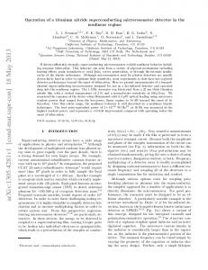
FIG. 1. SEM micrographs of superconducting niobium nitride nanowires and nanoribbons synthesized by annealing NbSe3 nanostructure precursors in flowing ammonia gas at 950 ° C for 2 h. Images at low and high magnifications are presented in 共a兲 and 共b兲, respectively.
molecular nitrogen can only take place at temperatures above 1400 ° C,25,26 and niobium is very reactive with oxygen. The second route, annealing the NbSe3 nanostructures in flowing ammonia gas at 700– 1000 ° C, resulted in a gray product which exhibited the presence of superconductivity. The morphology of the precursors and final samples was analyzed with a scanning electron microscope 共SEM兲 共Hitachi S-4700-II兲. Figure 1 shows SEM micrographs for the NbSe3 nanostructures annealed at 950 ° C for 2 h. Wires and ribbons of various sizes can be seen. This size distribution of the annealed wires and ribbons follows that of the precursor NbSe3 nanostructures which have transversal dimensions ranging from ⬃20 nm to a few micrometers and lengths up to millimeters.24 Remarkably, the high annealing temperature 共up to 1000 ° C兲 did not result in the collapse of the shape of the NbSe3 nanostructures. It is possible that NbSe3 first decomposes 共NbSe3 → Nb+ Se兲 and then Nb reacts with the ionic nitrogen to form niobium nitrides 共Nb+ NH3 → NbNx + H2兲. In fact, we noticed a red coloration of the exhaust line associated with selenium. A high magnification SEM micrograph shown in Fig. 1共b兲 reveals that the annealed wires and ribbons contain a high density of defects such as holes and gaps between grains, indicating their polycrystallinity. We used powder x-ray diffraction 共XRD兲 共Rigaku, model Miniflex, Cu K␣兲 to identify the phases of the synthesized materials. Figure 2 delineates the XRD patterns of the NbSe3 nanostructures after annealing for 2 h at 765, 840, 910, 950, and 1000 ° C. No traces of the NbSe3 phase are observed. All the diffraction peaks for the NbSe3 nanostructures annealed at 765 ° C can be indexed to a Nb4N5 phase while peaks associated with a Nb5N6 phase appear in the XRD patterns for those annealed at 840 ° C and above. A superconducting quantum interference device magnetometer was used to characterize the superconductivity of the converted niobium nitride nanostructures 共in the amount of milligrams兲. The temperature dependence of the magnetization for the samples processed at the aforementioned anneal-
Appl. Phys. Lett. 91, 162508 共2007兲
FIG. 2. 共Color online兲 Structural and magnetization analyses of the niobium nitride nanostructures synthesized at various annealing temperatures. 共a兲 Powder x-ray diffraction patterns and 共b兲 magnetization vs temperature curves 共measured at 0.1 G兲.
ing temperatures is presented in Fig. 2共b兲. The superconducting critical temperature 共Tc兲 increases from ⬃2.5 to 9.7 K when the annealing temperature is raised from 765 to 1000 ° C. Furthermore, the superconducting transition becomes sharper for samples synthesized at lower temperatures. Interestingly, there are more than two distinct critical temperatures despite the fact that XRD analyses reveal only Nb4N5 and Nb5N6 phases. This can be understood from the fact that niobium nitrides are always nitrogen deficient and Tc is highly sensitive to slight changes in the crystalline lattice parameters.25 From the XRD and magnetization data, we surmise that Nb4N5 represents the lower Tc 共up to ⬃7 K兲 phase which dominates the samples sintered at 910 ° C and below, while the Nb5N6 phase has higher Tc and is the main component of the samples obtained at 950 and 1000 ° C. Four-probe transport measurements were conducted to investigate the superconductivity of individual nanowires and nanoribbons. Electrical contacts were fabricated using photolithography and lift-off techniques. Figure 3共a兲 shows the temperature dependence of the resistance for three nanowires synthesized at 950 ° C. The resistance was normalized to their values at 14 K. The critical temperature 共Tc兲, defined with a resistance criterion of 90% RN, is 9.05, 9.4, and 11.2 K for samples A, B, and C, respectively. It indicates that the superconducting properties vary from wire to wire even under the same synthesis conditions. This variation cannot originate from the size effect since the diameters of all the three wires are a few hundred nanometers, which are much larger than the zero-temperature superconducting coherence length of niobium nitride, typically 3 – 5 nm.27 It is most likely due to the slight difference in nitrogen stoichiometry among the different wires. In fact, the two-step superconducting transition found in samples A and C indicates that the nitrogen stoichiometry is probably inhomogeneous even within the same wire. This is consistent with the observation of two phases in the XRD pattern given in Fig. 2共a兲. We carried out further measurements on sample B which showed
Downloaded 23 Jun 2008 to 146.139.245.69. Redistribution subject to AIP license or copyright; see http://apl.aip.org/apl/copyright.jsp
162508-3
Appl. Phys. Lett. 91, 162508 共2007兲
Patel et al.
3共c兲兴. As shown in the inset of Fig. 3共c兲, I*共T兲 exhibits the typical parabolic form expected for hot-spot effect related to thermal heating.28 Since the cross-sectional dimension of sample B is much larger than the superconducting coherence length, the phase slips observed in narrower superconducting nanowires should not occur in our sample at low temperatures. Thus, the hot spots in our samples are most likely caused by defects. This material is based upon work supported by the U.S. Department of Energy, Award No. DE-FG02-06ER46334 and Contract No. DE-AC02-06CH11357. S.A. and Z.X. also acknowledge support from the National Science Foundation 共NSF兲 under Award No. DMR-060762. SEM analysis and photolithography nanocontacting were performed at Argonne’s Electron Microscopy Center 共EMC兲 and Center for Nanomaterials 共CNM兲, respectively. A. Bezryadin, C. N. Lau, and M. Tinkham, Nature 共London兲 404, 971 共2000兲. 2 C. N. Lau, N. Markovic, M. Bockrath, A. Bezryadin, and M. Tinkham, Phys. Rev. Lett. 87, 217003 共2001兲. 3 M. L. Tian, J. G. Wang, J. S. Kurtz, Y. Liu, M. H. W. Chan, T. S. Mayer, and T. E. Mallouk, Phys. Rev. B 71, 104521 共2005兲. 4 M. Tian, N. Kumar, S. Xu, J. Wang, J. S. Kurtz, and M. H. W. Chan, Phys. Rev. Lett. 95, 076802 共2005兲. 5 D. S. Hopkins, D. Pekker, P. M. Goldbart, and A. Bezryadin, Science 308, 1762 共2005兲. 6 J. J. Palacios, Phys. Rev. B 57, 10873 共1998兲. 7 A. Falk, M. M. Deshmukh, A. L. Prieeto, J. J. Urban, A. Jonas, and H. K. Park, Phys. Rev. B 75, 020501 共2007兲. 8 G. Yi and W. Schwarzacher, Appl. Phys. Lett. 74, 1746 共1999兲. 9 D. Y. Vodolazov, F. M. Peeters, L. Piraux, S. Matefi-Tempfli, and S. Michotte, Phys. Rev. Lett. 91, 157001 共2003兲. 10 S. Michotte, S. Matefi-Tempfli, and L. Piraux, Appl. Phys. Lett. 82, 4119 共2003兲. 11 M. L. Tian, J. G. Wang, J. Snyder, J. Kurtz, Y. Liu, P. Schiffer, T. E. Mallouk, and M. H. W. Chan, Appl. Phys. Lett. 83, 1620 共2003兲. 12 A. Rogachev and A. Bezryadin, Appl. Phys. Lett. 83, 512 共2003兲. 13 Y. L. Wang, X. C. Jiang, T. Herricks, and Y. N. Xia, J. Phys. Chem. B 108, 8631 共2004兲. 14 Z. L. Xiao, C. Y. Han, W. K. Kwok, H. H. Wang, U. Welp, J. Wang, and G. W. Crabtree, J. Am. Chem. Soc. 126, 2316 共2004兲. 15 Y. Y. Wu, B. Messer, and P. D. Yang, Adv. Mater. 共Weinheim, Ger.兲 13, 1487 共2001兲. 16 Q. Yang, J. Sha, X. Y. Ma, Y. J. Ji, and D. R. Yang, Supercond. Sci. Technol. 17, L31 共2004兲. 17 M. Nath, and M. B. A. Parkinson, Adv. Mater. 共Weinheim, Ger.兲 18, 2504 共2006兲. 18 Y. S. Hor, U. Welp, Y. Ito, Z. L. Xiao, U. Patel, J. F. Mitchell, W. K. Kwok, and G. W. Crabtree, Appl. Phys. Lett. 87, 142506 共2005兲. 19 Y. G. Li and L. Gao, J. Am. Ceram. Soc. 86, 1205 共2003兲. 20 A. Korneev, P. Kouminov, V. Matvienko, G. Chulkova, K. Smirnov, B. Voronov, G. N. Gol’tsman, M. Currie, W. Lo, K. Wilsher, J. Zhang, W. Slysz, A. Pearlman, A. Verevkin, and R. Sobolewski, Appl. Phys. Lett. 84, 5338 共2004兲. 21 A. J. Kerman, E. A. Dauler, W. E. Keicher, J. K. W. Yang, K. K. Berggren, G. Goltsman, and B. Voronov, Appl. Phys. Lett. 88, 111116 共2006兲. 22 J. Kawamura, R. Blundell, C. E. Tong, G. Goltsman, E. Gershenzon, and B. Voronov, J. Appl. Phys. 80, 4232 共1996兲. 23 M. Hajenius, J. J. A. Baselmans, J. R. Gao, T. M. Klapwijk, P. A. J. de Korte, B. Voronov, and G. Gol’tsman, Supercond. Sci. Technol. 17, S224 共2004兲. 24 Y. S. Hor, Z. L. Xiao, U. Welp, Y. Ito, J. F. Mitchell, W. K. Kwok, and G. W. Crabtree, Nano Lett. 5, 397 共2005兲. 25 M. Gurvitch, J. P. Remeika, J. M. Rowell, J. Geek, and W. P. Lowe, IEEE Trans. Magn. 21, 509 共1985兲. 26 C. C. Agrafiotis, J. A. Puszynski, and V. Hlavacek, J. Am. Ceram. Soc. 74, 2912 共1991兲. 27 T. Ohashi, H. Kitano, A. Maeda, H. Akaile, and A. Fujimaki, Phys. Rev. B 73, 174522 共2006兲. 28 A. V. Gurevich, Rev. Mod. Phys. 59, 941 共1987兲. 1
FIG. 3. 共Color online兲 Four-probe transport measurements of individual niobium nitride nanowires measured with a current of 10 A. 共a兲 Zero field R vs T curves of three nanowires 共denoted samples A, B, and C兲. Inset to 共a兲 contains H-T phase diagrams of sample B as prepared 共open circles兲 and exposed to air for 3 weeks 共open triangles兲. 共b兲 and 共c兲 are R-H curves at various fixed temperatures and zero-field I-V curves at various fixed temperatures for sample B, respectively. Inset to 共c兲 presents the temperature dependence of the current I* at which the voltage increases abruptly.
no apparent two-step transition to study the superconducting properties of the niobium nitride nanostructures. The diameter of sample B is ⬃650 nm and the superconducting transition width 共temperature difference at 10% RN and 90% RN兲 is 0.9 K. The distance between voltage leads is 5 m. The superconducting phase diagram, H共T兲, for sample B obtained by measuring the resistance versus temperature curves in various magnetic fields with a current of 10 A is shown in the inset of Fig. 3共a兲, where the applied magnetic field is perpendicular to the long axis of the wire. The superconducting coherence length of 0 = 6.5 nm, determined from dHc2 / dT = −0.82 T / K, is consistent with typical values for niobium nitride.27 In order to examine the stability of the wire in atmosphere, we remeasured sample B after leaving it exposed to air for 3 weeks. The superimposed phase diagrams 关Fig. 3共a兲 inset, open circles and open triangles兴 indicate that its superconducting properties were not affected by the exposure to air. As discussed in the introduction, superconducting nanowires and nanoribbons can be an ideal system to explore properties of few-row vortex lattice. In transport measurements, the critical current and resistance are predicted to oscillate with sweeping magnetic field which leads to a change in the number of rows and rearrangement of the vortex lattice. We find in sample B an oscillation in the resistance versus magnetic field curves obtained at temperatures close to Tc 关Fig. 3共b兲兴. Furthermore, voltage jumps also appear in the I-V characteristics at low temperatures in sample B 关Fig.
Downloaded 23 Jun 2008 to 146.139.245.69. Redistribution subject to AIP license or copyright; see http://apl.aip.org/apl/copyright.jsp