Towards A Legged Chip Timir Datta and Pamela Abshire
John A. Turner
Department of Electrical and Computer Engineering Institute for Systems Research University of Maryland, College Park College Park, MD, USA {tdatta, pabshire}@umd.edu
Department of Electrical and Computer Engineering Virginia Polytechnic Institute and State University Blacksburg, VA, USA
[email protected]
Abstract—We describe a substrate for a Legged Chip, a CMOS integrated circuit with built in actuation mechanisms for motion. We have designed and fabricated a custom integrated circuit using a commercial 0.5μm CMOS technology which implements walking gait control. The circuit specifications and physical implementation have been designed to take into consideration the addition of thermal actuators through lowtemperature MEMS surface processing on fabricated CMOS dies. External connections will be limited to two leads for providing power and ground. This work represents progress towards a fully autonomous mobile integrated circuit.
I.
INTRODUCTION
Although mobile microrobots have long been a popular subject for science fiction, they are now edging closer to reality. There are a myriad of potential uses, from surveillance to manufacturing to infrastructure monitoring to healthcare. One of the proposed approaches for their development is integration with Complementary Metal Oxide Semiconductor (CMOS) circuits for sensing and control, and thus much of the early work in this area has focused on the fabrication of Micro Electro Mechanical Systems (MEMS) on silicon substrates that provide actuation and might serve as “legs” [1], [2], [3], [4]. Another body of work has focused on the design of driving circuits which perform the necessary computation and provide signals for controlling such systems [5], [6], [7], [8]. It is desirable that a complete realization of a microrobot incorporate both the mechanical systems as well as the electrical systems; however, most existing implementations rely on large scale robotics [9], [10], or on miniaturization of existing technologies [11], [12], and do not satisfy the requirement of an all inclusive microrobot system that can be scaled down to even smaller dimensions. One notable exception is the work of Hollar et al., which integrated control, actuation, and power generation at the micro scale in order to create an un-tethered silicon microrobot [13]. This system was successfully demonstrated despite a number of significant technical challenges [13]: three different processes were used to create the robot, a 0.25μm process for the control Integrated Circuit (IC), a high voltage Silicon On Insulator (SOI) process for the solar cells, and a proprietary SOI-based MEMs process for fabrication of the motors and actuators. In this work we present the first of a two part development for a novel microrobot with integrated control and actuation.
978-1-4244-9474-3/11/$26.00 ©2011 IEEE
II.
MECHANICAL SYSTEMS OVERVIEW
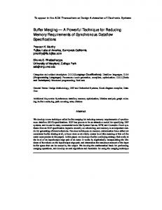
A. Microrobot Design Considerations The microrobot will be comprised of a CMOS integrated circuit die with MEMS thermal actuators to serve as “legs”. The actuators will be implemented as bi-material strips with a large difference in coefficient of thermal expansion (CTE) between the two materials. Power delivery and programming will be done through externally connected leads. The physical implementation of the integrated circuit has been designed so as to facilitate post fabrication of the necessary actuators, and to ensure that the control and driving circuits can support the large power draw and resulting heat associated with operation of the actuators. Fig. 1 shows a photomicrograph of the fabricated IC overlaid with a sketch of the thermal actuators. The dimensions are 3 mm by 1.5 mm, with the active area of the chip inset by 250μm on all sides so as to leave a buffer space for clean room processing.
Figure 1: Chip photomicrograph showing four sets of thermal actuators (blue/yellow overlay) with power pads at opposite edges.
B. Walking Gait and Control As described above, the “legs” for this chip are intended to be MEMS thermal actuators. As shown in Fig. 1, there are four groups of thermal actuators which are intended to be operated in two sets (ABAB, see Fig. 2) as in [4]. Given the limited degree of freedom in the movement of the “legs,” the gait of the microrobot must be controlled to allow relatively efficient motion. The waveforms which will be applied to the actuators and the resultant gait are shown in Fig. 2. The actuators are grouped into two sets, A and B. All actuators in
2501
set A receive the same input; similarly all actuators in set B receive the same input. There are four control states (1-2-3-4, see Fig. 2) which can be applied in succession to induce motion. In State 1, both actuation signals are low, and neither pair of actuators is on. In State 2, signal A is high and signal B is low, resulting in a linear displacement of the microrobot. In State 3, both signals are high and the position is maintained. In State 4, signal A transitions to low, signal B remains high, and again the position is maintained. Finally the transition from State 4 back to State 1 results in another linear displacement.
expected to be 51.5 μN. Calculation of the expected blocked force given design constraints is shown below. Eqn (1) [14] shows the force F at the tip of the cantilever as a function of the moment M and aspect ratio W/L. Eqn (2) [14] shows the moment M as a function of metal thickness hmet, ratio of material thicknesses m=hpoly/hmet, ratio of residual stress from deposition n=Epoly/Emet, and inherent strain in the polymer αpoly. Using these equations the blocked force for a “leg” with a ¼ aspect ratio is found to be 12.5 μN. Given that there will be six legs supporting the structure at any given time, the total force (75 μN) exceeds the minimum requirement. ଷெ ௐ ܨൌ ቀ ቁ (1) ଶ
ܯൌ
Figure 2: Gait profile of the “legs,” and associated waveforms which will be applied to the actuators.
C. Thermal Actuators As previously mentioned, the “legs” will be thermal actuators (Fig. 3). Although these actuators are inefficient due to significant heat losses, they are also known to provide high force per unit area. Actuator efficiency is not a concern since power is supplied externally. These actuators will be fabricated on top of the passified (glass) surface of the nonpackaged CMOS IC die. The materials used for the thermal bilayer will be the epoxy based photoresist SU-8 (MicroChem Corp) and Cu. Since the two materials have very different CTEs, any significant change in temperature will result in a bending force. This change in temperature will be induced by applying a relatively large current to the copper material. The actuators can be modeled as small resistors; measurements made on previously fabricated actuators show resistance and current requirements of approximately 10 Ω and 150mA per actuator, respectively. Given the limited current carrying capability of the CMOS process, each pair of actuator sets is powered in series, so that the maximum current through the system would be limited to 300mA. Due to the freely moving nature of the cantilevers, the only relevant friction forces are those encountered by the tip when fully extended; the system is not expected to move in the absence of friction forces at the tips. One significant constraint which is imposed by the use of thermal actuators is that they will need to cool off between actuation cycles. The cooling time will be proportional to the difference in actuator temperature and ambient air, and we anticipate that it may be necessary to run the microrobot on a cooled surface.
మ ሺଵାሻఈ ா
ଶሺଵାሻ
(2)
Figure 3: Sketch of one thermal actuator, showing the insulating polymer material and metal trace (left) and the bilayer which experiences a bending force when heated (right).
D. Duty Cycle Modulation Given uncertainty in the dynamics of the yet to be fabricated “legs,” we have implemented a duty cycle modulation scheme using two externally controlled pads with digital (HI/LO) inputs. These pads will be connected externally to POWER or GROUND via a metal trace (ideally, fabricated using the same process sequence as the “legs” themselves) and will provide for three different types of duty cycles for controlling the two sets of actuators, illustrated in Fig. 4. Configuration 1 will result in 10% duty cycles for both signals A and B, and will result in no overlap between the two signals. Configuration 2 will result in 20% duty cycles for each signal with an overlap of 50% of the on-time (10% of the total cycle). Configuration 3 will also result in 10% duty cycles for each signal and will have a 50% on-time overlap (5% of the total cycle).
Figure 4: Three different duty cycle configurations for the thermal actuators.
The thermal actuators have been designed to provide enough force to support the weight of the CMOS IC, which is
2502
Figure 5: System overview
The rationale behind these choices are as follows: (1) the thermal actuators will likely take longer to cool off than they will to heat, thus control waveforms for each set of actuators are “on” for only 10% or 20% of the total cycle time; (2) one set of actuators should come on and turn off sooner than the other set, and the natural temporal asymmetry between the heating and cooling processes will support this phasing, thus control waveforms have relative phasing of 0%, 5%, and 10% of the total cycle time. It is hoped that one of these configurations will allow for optimum movement of the microrobot. III.
ELECTRONICS OVERVIEW
The circuits included in the CMOS IC include a modified Integrate and Fire Neuron (I&F Neuron) for low frequency pattern generation, Floating-Gate (FG) programming for control of the overall duty cycle, bias circuits, simple logic for generating control signals, and actuator drivers. Fig. 5 shows an overview.
B. Frequency Programming External adjustment of the overall cycle time for driving the actuators is possible through the use of a floating gate current source. Control signals to decrease or increase the frequency, by increasing or decreasing the voltage on an oxide isolated floating node respectively, are applied through two externally connected leads. These control signals are required only during setup, and thus will be unconnected during normal operation of the microrobot. Fowler-Nordheim tunneling is used to increase the floating gate potential, and impact-ionized hot electron injection is used to decrease the potential [15]. The floating gate potential cannot be directly measured, and must be inferred from the observed driving frequency. C. Bias Circuits Floating-gate current sources coupled with current division techniques [16] were used to generate the low bias currents required for slow spiking rates of the I&F Neuron. Currents on the order of 10 pA provide the necessary oscillation rates specified in the design. A floating-gate programmable current mirror provides the initial current which is then divided to produce the appropriate magnitude. Use of a floating-gate current source allows for programmability of the oscillation rates after fabrication to account for any unforeseen mechanical effects.
A. Pattern Generator Pattern generation for driving the actuators is done using a modified I&F Neuron with low spiking rates (see Fig. 6). The output of the I&F Neuron is a sawtooth wave between 0 and 1V which is compared to two different DC bias voltages in order to generate each control signal as shown in Fig. 7. The resultant digital waveforms are used to drive the actuators. A simulation of the driving waveforms is shown in Fig. 8.
Figure 8: Current driving signals for the two sets of thermal actuators, as produced by pattern generator.
D. Actuator Drivers To power each set of thermal actuators, a current of 150mA must be generated. Due to the high and unpredictable operating temperature for this chip, use of a simple PMOS current source could result in a wide range of currents and resulting actuator responses. To generate a constant current with little temperature dependence [17], the gate of an NMOS transistor was biased at approximately the isotemperature point for the transistor. The isotemperature point was determined experimentally for transistors in the fabrication technology to be 1.1V (see Fig. 9). This known current was scaled up through a series of current mirrors to produce the desired temperature-independent 150mA bias current.
Figure 6: Schematic for I&F Neuron sawtooth generator.
Figure 7: Signal Generator: sawtooth plus comparators that generate control signals as shown in Figure 4.
2503
design was initiated as a project in a mixed signal VLSI design class by undergraduate students Robert Bailey, Benjamin Chang, Angel Diaz, and Daniel Sher. We thank the ECE department for providing the facilities necessary to conduct the work and MOSIS for providing the opportunity to fabricate the circuit. This material is based upon work supported by the National Science Foundation under Award No. 0931878. REFERENCES [1]
[2] Figure 9: Experimental I-V characteristics for 600/6 NMOS illustrating isotemperature point of 1.1V.
E. Layout Considerations Given the unique nature of the design and the requirement for MEMS post fabrication, a custom padframe was used for this design. 10 large pads around the periphery of the chip were used to facilitate connection of external leads, and all busses for high current signals were built with a 2X safety margin, theoretically allowing them to carry twice the required current before effects such as electro-migration come into play. Eight of those pads are connected to terminals of MEMS components and internally within the circuit to drive the MEMS thermal actuators, and only the power and ground pads at opposite ends of the chip will be tethered to a power supply during operation. In addition to the 10 large pads, there are four small pads at the ends of the chip which provide for duty cycle selection and FG programming as described above. The duty cycle selection pads are at the left edge of the chip, and the FG programming pads are at the right edge as observed in Fig. 1. IV.
[3]
[4]
[5]
[6]
[7]
[8]
[9]
[10]
CONCLUSION
We have designed and simulated a CMOS IC for integration with MEMs actuators as a “legged chip”. The IC contains on-board timing signal generation for actuation, and includes wide metal traces for providing large driving currents to thermal actuators. Actuation frequency and relative dutycycle and overlap are programmable via external control signals which can be readily hardwired into the physical implementation during MEMS fabrication. The design has been fabricated in a standard commercially available 0.5μm CMOS technology. In future collaboration with the Laboratory for Microtechnologies at UMD, MEMS thermal actuators will be post fabricated onto the IC and the prototype microrobot will be tested.
[11]
[12]
[13]
[14]
[15]
ACKNOWLEDGMENT We would like to thank members of the Integrated Biomorphic Information Systems Laboratory and the Laboratory for Microtechnologies at UMD, with special thanks to Elisabeth Smela and Bavani Balakrishnan for their support and helpful input regarding the actuators. This chip
[16]
[17]
2504
M.H. Mohebbi, M.L. Terry, K.F. Böhringer, G.T.A. Kovacs, and J.W. Suh, “Omnidirectional walking microrobot realized by thermal microactuator arrays,’’ in Proc. ASME Int. Mech. Eng. Cong. & Exp., pp. 1–7, Nov. 2001. P.E. Kiaditis, V.M. Bright, K.F. Harsh, and Y.C. Lee, “Prototype microrobots for micro positioning in a manufacturing process and micro unmanned vehicles,” 12th IEEE Int’l. Conf. on Micro Electro Mech. Syst. (MEMS '99), pp.570-575, Jan. 1999. K. Suzuki, I. Shimoyama, and H. Miura, “Insect-model based microrobot with elastic hinges,” J. Microelectromech. S., vol.3, no.1, pp. 4-9, Mar. 1994. T. Ebefors, J. Mattsson, E. Kalvesten, and G. Stemme, ‘‘A walking silicon micro-robot,’’ 10th Int’l. Conf. Solid-State Sensors and Actuators (Transducers’99), Sendai, Japan, pp. 1202---5, June. 1999. J.H. Cho and M.G. Arnold, “Powering embedded CMOS logic on MEMS-based micro-robots,” IEEE Behavioral Modeling and Simulation Workshop (BMAS 2009), pp.73-77, 17-18 Sept. 2009. K. Nakada, T. Asai, and Y. Amemiya, “An analog CMOS chip implementing a CNN-based locomotion controller for quadruped walking robots,” Proc. 2004 Int’l. Symp. Circuits and Systems (ISCAS '04), vol.3, pp. III- 1-4, 23-26 May. 2004. M.A. Lewis, R. Etienne-Cummings, A.H. Cohen, and M. Hartmann, “Toward biomorphic control using custom aVLSI CPG chips,” Proc. IEEE Int’l. Conf. Robot. & Autom. (ICRA '00), vol.1, pp.494-500, 2000. M.A. Lewis, F. Tenore, and R. Etienne-Cummings, “CPG Design using Inhibitory Networks,” Proc. 2005 IEEE Int’l. Conf. Robotics and Automation (ICRA 2005), pp. 3682- 3687, 18-22 April. 2005. S. Still, K. Hepp, and R.J. Douglas, “Neuromorphic walking gait control,” IEEE Trans. Neural Networks, vol.17, no.2, pp.496-508, March. 2006. S. Still, B. Schölkopf, K. Hepp, and R. Douglas, “Four-legged walking gait control using a neuromorphic chip interfaced to a support vector learning algorithm,” Advances in Neural Information Processing Systems, vol. 13, pp. 741- 747, 2000. R.H. Byrne et al., “Miniature Mobile Robots for Plume Tracking and Source Localization Research,” J. Micromechatronics, vol. 1, no. 3, pp. 253-261, 2002. G. Caprari, K.O. Arras, and R. Siegwart, “The autonomous miniature robot Alice: from prototypes to applications,” in IEEE/RSJ Int’l. Conf. Intelligent Robots and Systems (IROS ’00), pp. 793-798, 2000. S. Hollar, A. Flynn, C. Bellew, and K.S.J. Pister, “Solar powered 10 mg silicon robot,” 16th Ann. Int’l. Conf. on Micro Electro Mechanical Systems (MEMS03), Kyoto, pp. 706- 711, 19-23 Jan. 2003. B. Shapiro, and E. Smela, “Bending Actuators with Maximum Curvature and Force and Zero Interfacial Stress,” J. Intelligent Material Systems and Structures, vol. 18, no. 2, pp. 181-186, Feb. 2007. P. Hasler, B. Minch, and C. Diorio, “An autozeroing floating-gate amplifier,” IEEE Trans. Circuits Syst. II, vol. 48, no. 1, pp. 74–82, Jan. 2001. T. Delbrück and A. Van Schaik, “Bias Current Generators with Wide Dynamic Range,” Analog Integrated Circuits and Signal Processing, vol. 43 , no. 3, pp. 247 – 268, June. 2005. I.M. Filanovsky and Su Tam Lim, “Temperature sensor applications of diode-connected MOS transistors,” Proc. 2002 Int’l. Symp. Circuits Syst. (ISCAS ’02), vol. 2, pp. 149 -152, May. 2002.