Nov 26, 2007 - arXiv:cond-mat/0607343v2 [cond-mat.mes-hall] 26 Nov 2007. Transmission through a biased graphene bilayer barrier. Johan Nilsson,1 A. H. ...
Transmission through a biased graphene bilayer barrier Johan Nilsson,1 A. H. Castro Neto,1 F. Guinea,2 and N. M. R. Peres3
arXiv:cond-mat/0607343v2 [cond-mat.mes-hall] 26 Nov 2007
1
Department of Physics, Boston University, 590 Commonwealth Avenue, Boston, MA 02215, USA 2 Instituto de Ciencia de Materiales de Madrid, CSIC, Cantoblanco E28049 Madrid, Spain 3 Center of Physics and Departamento de F´ısica, Universidade do Minho, P-4710-057, Braga, Portugal (Dated: September 17, 2007)
We study the electronic transmission through a graphene bilayer in the presence of an applied bias between layers. We consider different geometries involving interfaces between both a monolayer and a bilayer and between two bilayers. The applied bias opens a sizable gap in the spectrum inside the bilayer barrier region, thus leading to large changes in the transmission probability and electronic conductance that are controlled by the applied bias. PACS numbers: 81.05.Uw 73.21.Ac
I.
INTRODUCTION.
The idea of carbon based electronics has been around since the discovery of carbon nanotubes almost fifteen years ago. Much progress has been made but many problems associated with manufacturability remain still to be resolved – see for example the recent reviews in Refs. 1,2. Recently, another possible platform for carbon based electronics was discovered in graphene,3 i.e., a two-dimensional (2D) honeycomb lattice of carbon atoms that can be viewed either as a single layer of graphite or an unrolled nanotube. The electric field effect has already been demonstrated in these systems: by tuning a gate bias voltage one can control both the type (electrons or holes) and the number of carriers.4,5 For a recent review on the rise of graphene see Ref. 6. One fundamental difficulty with most of the graphene devices studied so far is the experimental fact that there exists a universal (sample independent) maximum in the resistivity of the order of 6.5kΩ near the Dirac point in all these systems.4 This relatively small resistivity limits the performance of devices via a poor on-off ratio. The reason for the nonzero minimal conductivity is the peculiar gapless spectrum and presence of disorder in the samples. Several theoretical studies using different methods find a universal minimum in the conductivity in some limits. But the reason for it and its exact value varies,7,8,9,10,11,12,13,14 see also the recent review Ref. 15. There has also been a number of earlier theoretical studies of junctions and barriers in both monolayer and bilayer graphene systems.9,13,16,17,18,19 One way of getting around the minimal conductivity is to use nano-ribbons made out of graphene. Because of the confinement these systems are generally found to be gapped,20 which is consistent with recent experiments.21 In this paper we propose another simple geometry that transforms the semi-metallic graphene into a semiconductor with a truly gapped spectrum without confinement. The presence of a gap makes the properties of the system more robust to perturbations. This is crucial for device performance and possible device integration since imperfections are always present. The basic idea is to
use a bilayer region as a barrier for the electrons. By manipulating the electrostatics with gates and/or chemical doping a gap can appear in the spectrum. By tuning the chemical potential one can move the system from sitting inside of the gap, where the electronic transmission is exponentially suppressed, into the allowed band regions where the transmission is close to one. Other interesting features of the proposed geometry are that the gap size can be tuned with gates, allowing for an external control of the electronic properties, and the bilayer can be integrated as one of the components of a pure graphene based device.22 Recently barriers made out of double-gated bilayer graphene have been fabricated and characterized in Ref. 23, and their results are consistent with a gate-tunable gap. The paper is organized as follows: In Section II we introduce the model of the system that we are considering and give explicit expressions for the wave functions. In Section III we match wave functions considering different geometries. In particular we study a monolayer-bilayer interface, a bilayer-bilayer interface, and two bilayer barrier setups. In the barrier setups we use either monolayer graphene or bilayer graphene in the leads. In Section IV we present results for the conductance in the different barrier setups. A brief summary and the conclusions of the paper can be found in Section V. For completeness we also provide some details about the self-consistent determination of the gap in Appendix A. In Appendix B we provide some details of how we compute the transmission amplitudes.
II.
MODEL
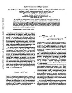
A schematic picture of the system is shown in Fig. 1. The basic structure involves a graphene sheet extending to the left and to the right of a region where there is a second graphene sheet sitting on top of the first, this region is the bilayer barrier (BB) region. The whole structure is assumed to sit on top of a dielectric spacer insulating the graphene from a back gate. Later on (Sec. III E) we will also consider a system where the regions to the left
2
FIG. 1: [color online] Geometry of the biased graphene bilayer barrier with monolayer leads.
and right of the barrier are made out of graphene bilayers. We will refer to the two systems as having monolayer and bilayer leads respectively. To the left (L) and to the right (R) of the barrier the low-energy effective Hamiltonian (near the K point of the Brillouin zone) has the form of the 2D Dirac Hamiltonian:24 � � Vα /vF kx + iky , (1) Hα = vF kx − iky Vα /vF where k = (kx , ky ) is the 2D momentum measured relative to the K point, α = L, R and vF ≈ 106 m/s is the Fermi-Dirac velocity (we use units such that h ¯ = 1 = vF from now on). The Dirac Hamiltonian acts on a spinor representing the wave functions on the two sublattices: ψ = (ψA1 , ψB1 )T . In the following, we mostly work with the case where VL = VR = 0 so that the energy is measured with respect to the Dirac point in the monolayer regions. The spectrum of the Hamiltonian in Eq. (1) is then simply E± (k) = ±k, (k 2 = kx2 + ky2 ), where the plus (minus) sign is associated with electron (hole) states. The low-energy effective bilayer Hamiltonian has the form [see e.g. Refs. 25,26]:
HBB
V1 qx + iqy t⊥ 0 V1 0 0 q − iqy = x . t⊥ 0 V2 qx − iqy 0 0 qx + iqy V2
(2)
Here the two-dimensional momentum is q = (qx , qy ) and the corresponding spinor is ψ = (ψA1 , ψB1 , ψA2 , ψB2 )T . t⊥ ≈ 0.35 eV is the hopping energy between nearest neighbor atoms in different planes (i.e., A1 and A2). The monolayer is connected to plane 1 in the bilayer. Solving for the spectrum of the Hamiltonian in Eq. (2) one finds four energy bands given by E±,s (q) = (V1 + V2 )/2 r q t2 1 V2 + ⊥ +s 4(V 2 + t2⊥ )q 2 + t4⊥ , (3) ± q2 + 4 2 2
where s = ± and V = V1 − V2 . Thus for the two bands closest to the Dirac point (E±,− ) the spectrum is gapped and has an unusual “Mexican hat” dispersion as was pointed out in Ref. 25. There exists other examples in the literature of materials with a similar dispersion, often called “camel-back”-dispersion instead of “Mexican hat”. This feature can arise – like in our case – in the k · p approximation when two bands that are close to each other in energy are allowed to hybridize. Examples of materials where a camel-back has been proposed include Tellurium,27 GaP,28 and GaAs.29 The crucial property for the structure proposed here is that we allow for different voltages on the two layers in the BB region: V1 6= V2 . This possibility have been noted before,25,30 but here we are exploiting this feature. These potentials can be created by a uniform electric field through the bilayer that generates a charge imbalance between the two layers. In a transport measurement the graphene is connected to electron reservoirs and can hence become charged. When voltages are applied to the gates and the graphene structure charge is redistributed to minimize the total electrostatic energy. The problem is basically that of a capacitor. Upon studying the problem the bilayer must be viewed as a single unit since the planes are connected by orbital overlap. For example, the induced charge imbalance between the layers will screen the applied electric field; t⊥ also works against the applied field since it tends to equalize the densities in the two planes. A simple estimate of these effects is provided by a self-consistent Hartree theory [see Appendix A and Refs. 26,31]. For an isolated uncharged infinite bilayer we find that the net effect is to replace the applied voltage difference V by a smaller effective VMF . For some reasonable parameters [V < t⊥ and interlayer distance d ≈ 3.35 − 3.6 ˚ A32,33 ], VMF is down by a factor of order three compared with the bare value. In particular for an experimentally accessible voltage drop of 90 V over 300 nm we find an effective voltage difference of VMF ∼ 40 meV. This value might be improved upon incorporating a dielectric (e.g., SiO2 ) and/or using a thinner dielectric spacer. Thus it is not unreasonable to have VMF ∼ 100 meV. This estimate was done before we became aware of the measurements reported in Refs. 34 and 35. In the first of these references the gap is measured in ARPES to be as large as 200 meV, but the charge densities are also quite large in their case (n ∼ 1 − 6 · 1013 cm−2 ). In the second reference the maximum obtained gap is estimated to be ∼ 100 meV. The largest possible value of the gap is estimated to be ∼ 300 meV and is limited by the dielectric breakdown of the SiO2 . Experimentally the bias can be controlled by different methods. The conceptually simplest and most flexible method is to use a back gate and a top gate (like in a dual gate MOSFET geometry), preferably using split gates and therefore allowing for different gate voltages in the monolayer and bilayer regions. It is worth to mention
3 that local top gates have already been successfully fabricated on single-layer graphene samples.36,37,38,39 The field is progressing rapidly, since for example only a year ago no top gate had been reported in graphene systems. Moreover, very recently a top gate was also fabricated on bilayer graphene and characteristics consistent with a gate-tunable gap were reported.23 Another possibility is to change the chemical environment by depositing donor or acceptor molecules on top of the structure.34,35 These act like dopants in a semiconductor and allow for independent control of the bias and the chemical potential. Note however that this method always introduces impurities into the system with potentially important consequences.40 On symmetry grounds a more general Hamiltonian than the one in Eq. (2) is certainly allowed as discussed in Ref. 41 for the case of graphite. For example, the couplings γ3 and γ4 associated with electron hopping between carbon atoms that are not nearest neighbors in different layers, familiar to the graphite literature, are possible.32 In the BB the effects of these terms are less important than for the low-energy features in graphite since the gap is a robust feature in the low-energy spectrum of the BB. The electrostatic response in different sublattices within each layer is also likely to be different, that is, one should use VA1 6= VB1 etc. If the applied voltage difference is not too large compared with t⊥ the implications of this effect are presumably small. The applied field and the pressure from anything on the top of the structure will probably affect both the interlayer distance and the interlayer coupling. The details of the band structure including all the effects above is a very complicated problem that has yet to be studied. Nevertheless, we believe that the Hamiltonian in Eq. (2) correctly captures the main features of the spectrum, including the important formation of the gap in the spectrum near the Dirac point. In view of the large uncertainty in the parameters involved, it is meaningless to pursue a more complicated model at this point. The inclusion of the other parameters introduce no principal problems, but the analysis becomes more complicated. A.
The eigenvectors
The normalized energy E eigenvectors of Hα in Eq. (1) can be written as: � � 1 E − Vα v¯α = √ , (4) 2(E − Vα ) kx − iky when the particles are “on-shell”: (E − Vα )2 = kx2 + ky2 .
(5)
A simple way to generate the eigenvectors of HBB in Eq. (2) is to note that the columns of the Green’s func� �−1 tion G0 in the bilayer region (G0 = E − HBB ) are proportional to the eigenvectors if the relation between
the energy E and the momentum q are “on-shell”. It is straightforward albeit tedious to generalize this approach to the more general Hamiltonians discussed above. Using this we extract two different energy E eigenvectors of HBB as � � 2 2 2 (E − V ) (E − V ) − q − q 1 2 x y � � (E − V2 )2 − q 2 − q 2 (qx − iqy ) x y , (6) v¯BB,A1 = t⊥ (E − V2 )(E − V1 ) t⊥ (E − V1 )(qx + iqy ) and
v¯BB,A2
t⊥ (E − V2 )(E − V1 ) t⊥ (E − V2 )(qx −� iqy ) � = (E − V1 )2 − qx2 − qy2 (E − V2 ) . � � (E − V1 )2 − qx2 − qy2 (qx + iqy )
(7)
These just differ by their overall normalization. It is straightforward to check that these vectors are indeed eigenvectors of HBB in Eq. (2) by direct substitution. The “on-shell” condition in the bilayer region reads: 2(qx2 + qy2 ) = (E − V1 )2 + (E − V2 )2 q �2 � ± (E − V1 )2 − (E − V2 )2 + 4t2⊥ (E − V1 )(E − V2 ). (8) III.
DIFFERENT GEOMETRIES
In this section we compute the transmission amplitudes for different edges and geometries. By convention the incident wave is taken to arrive from the left side of the barrier and is transmitted to the right. A.
Zig-zag termination with monolayer leads
With our conventions the zig-zag termination of the barrier corresponds to cutting the strip along the ydirection. For simplicity we consider the case that the width W of the structure is large enough so that the boundary conditions in the transverse direction are irrelevant. It is then convenient to assume periodic boundary conditions and use translational invariance and fix ky = qy to be a good quantum number in addition to the energy E. This assumption can be relaxed.9,19,42 When the width becomes small enough that the quantization of the transverse momentum becomes important the system becomes similar to a semiconducting nanotube with a finite radius. As discussed by Brey and Fertig, it is a good approximation to use the continuum description of a graphene ribbon if it is wide enough and provided that the proper boundary conditions for the continuous model are employed.43 For the zig-zag edges one can work in the single valley approximation and the correct boundary condition is to take the wave-function to vanish in one of the sublattices (A2 on the left and B2 on the right in
4 our case) at the BB boundaries. We choose the energy E and ky = |E| sin(φ) so that there are propagating states to the left of the junction, with kx = E cos(φ). The four solutions of Eq. (8) for qx inside the bilayer we denote by ±qx1 and ±qx2 . B.
Monolayer-bilayer interface
Consider the step geometry where there is no right end of the bilayer. Then one must only keep states that propagate to the right or decay as one moves into the bilayer. Thus, to the left we take the wave function to be: ψ¯L = 1¯ vL,+ eikx x + r¯ vL,− e−ikx x ,
monolayer is coupled to layer 1 in the bilayer. When the energy is tuned to V1 the weight on sublattice A1 goes to zero [c.f. Eq. (7)]. Consequently the current in plane 1 is zero at that energy, and hence no current can flow into the bilayer. It appears as though the current goes continuously to zero as the band edge is approached. At the other edge (E ∼ V2 ) of the band gap the current in plane 2 is zero [c.f. Eq. (6)], but the current can now flow in through the other plane. This fact is responsible for the sharp edge in the transmission amplitude at the conduction band edge.
(9)
where r is the reflection amplitude, and v¯L± are the spinors associated with the sublattices given in Eq. (4). In the bilayer one has, ψ¯BB = a1+ v¯BB,1+ eiqx1 x + a2+ v¯BB,2+ eiqx2 x ,
(10)
where a1(2)± are scattering amplitudes and v¯BB,1(2)± the respective spinors computed from Eq. (6) or Eq. (7). Matching of the wave functions only involves their continuity. Because the associated differential equation is of first order this is sufficient to insure current conservation. Explicitly the boundary conditions are: ψ¯L (x = 0) A1 = ψ¯BB (x = 0) A1 , (11a) ¯ ¯ ψL (x = 0) B1 = ψBB (x = 0) B1 , (11b) ¯ ψBB (x = 0) A2 = 0. (11c)
From this we compute [for details see Appendix B] the transmission probability T (E, φ) = 1 − |r|2 and the angular averaged transmission probability T (E) =
Z
π/2 −π/2
dφ T (E, φ). π
(12)
Some representative results are shown in Fig. 2. There are two features that are apparent in the figure: (a) There is a small asymmetry between the angles ±φ. Hence, a current of electrons without valley polarization leads to a transmitted current with a finite valley polarization. This is not the case at other boundaries, like a potential step applied to a graphene monolayer or a graphene bilayer.17 The breaking of the symmetry between the two Dirac points arises from the lack of time reversal symmetry, as we consider a current carrying state, and the lack of inversion symmetry, induced by the zigzag bilayer edge or the bias potential in the bilayer (for a general discussion, see Ref. 44, for a particular discussion see Appendix B). As a result, the barrier discussed here can be used as a device which creates a valley polarized current.45 (b) There is a clear asymmetry between positive and negative energies. This can be understood by noting that the
FIG. 2: [color online] Transmission amplitudes in the monolayer-bilayer step geometry. Left: Energy dependence of T for V2 − V1 = 40 meV and different values of V1 . Right: Angular dependence of T (E, φ) for V1 = 10 meV and V2 = 50 meV and different values of the energy.
It is important to choose the momenta for right-movers in Eq. (9) and Eq. (10) such that their group velocity vg = dE/dqx > 0. Otherwise one may erroneously conclude that T < 0 for some values of the energy, this is sometimes referred to as the Klein paradox.46 It is also worth noting that the actual charge distribution near the edge is a complicated problem that involves a selfconsistent solution of the Poisson equation and the band structure, beyond the scope of this study. This may lead to corrections to the simple wave function matching we use here. Furthermore, it is known that edges can lead to interesting effects in graphene systems such as edge states and self-doping.7 C.
Biased bilayer barrier with monolayer leads
Consider the barrier geometry of Fig. 1. We assume the length L of the bilayer region to be large compared to the lattice spacing so that the continuum model is applicable. In this geometry one also needs the wave function to the right of the barrier: ψ¯R = t¯ vR,+ eikx (x−L) ,
(13)
where t is now the transmission amplitude. Inside the barrier one generally needs all momentum components: ψ¯BB = a1+ v¯BB,1+ eiqx1 x + a2+ v¯BB,2+ eiqx2 x + a1− v¯BB,1− e−iqx1 x + a2− v¯BB,2− e−iqx2 x . (14)
5 In this case, in addition to the boundary conditions in Eq. (11) there are also those at the right edge: ψ¯R (x = L) A1 = ψ¯BB (x = L) A1 , (15a) ψ¯R (x = L) B1 = ψ¯BB (x = L) B1 , (15b) ψ¯BB (x = L) B2 = 0. (15c)
It is a simple task to match the boundary conditions and in this case one finds six equations for the six unknowns: t, r, a1+ , a1− , a2+ , and a2− . The results for T (E, L, φ) = |t|2 for some representative parameters are shown in Fig. 3. The oscillations in the transmission amplitudes are due to the possibility of having resonances inside of the BB region. For example, in the right panel of Fig. 3 the two energies are chosen such that they have the same q 2 computed from Eq. (8) for the propagating mode. In one case (E = 5 meV), |E| sin(φ) = qy ≪ q and the resonances are pronounced with the distance between consecutive maxima approximately given by π/qx ∼ π/q ∼ 25 nm. In the other case (E = −45 meV), |E| sin(φ) = qy ∼ q and most of the resonance phenomena averages out upon performing the angle average because of the larger variation of qx .
FIG. 3: [color online] Transmission amplitudes in the BB with monolayer leads. Left: Energy dependence of T (E, L, φ) for different angles and L = 50 nm. Right: Length dependence of T (E, L) for different energies. In both the figures V1 = 0 and V2 = −40 meV.
D.
Armchair termination
The calculations for the armchair geometry is similar albeit more involved since one cannot work in the single cone approximation.43 In this case, one must instead mix the valleys to be able to fulfill the boundary conditions so that the wave functions on both of the lattice sites in layer 2 vanish at the boundaries. This doubles the size of the matrix problem that must be solved. For example, to compute the transmission amplitudes in the BB geometry one must solve a system of twelve equations. The calculation is a straightforward extension of the case above and although the shapes of the curves are not exactly the same there are no new features except for a parity effect associated with the number of unit cells in
the barrier. This is related to the modulo 3 effect found in the spectrum of an armchair graphene nano-ribbon in the nearest neighbor tight-binding approximation.43 E.
Bilayer-bilayer step and Biased bilayer barrier with bilayer leads
It is important to note that it is not necessary to have the BB region defined by actually cutting the second graphene sheet. Another possibility is to use a bilayer throughout, and to use a local top gate to create a local gap and hence a barrier in the bilayer. As we shall see, the characteristics of this type of junction is better than the one with the monolayer leads. In particular the oscillations in the transmission amplitudes and conductivities are much smaller because the matching between two bilayers is usually better than between a monolayer and a bilayer. We will consider the simple case that the bilayer in the L and R regions is essentially gapless, we also assume that |E| < t⊥ for the incoming wave as this will likely be the experimental situation. Since the gapless bilayer is a special case of the gapped bilayer with no gap we may use the formulas and spinors from Section II A directly with V1 = V2 = 0. This case was considered in Ref. 13 and allows for some further simplifications of the spinors, but that is not necessary here. The incoming wave is taken to be a traveling wave with absolute momentum given by k 2 = |E|(t⊥ + |E|). As in the above we define kx = ±k cos(φ) and ky = k sin(φ). One should also take care to define the sign of kx for the incoming wave so that the wave is a rightmover. We will denote the corresponding spinors by v¯B0,α , where α = ± goes with exp(±ikx x) and denotes right- and leftmovers respectively. To be able to fulfill the boundary conditions one must also consider the decaying modes,17 which will have an imaginary value of the momentum in the x-direction:qkx = iκx . One can show that the correct value is κx = |E|(t⊥ − |E|) + ky2 . The corresponding spinors we write as v¯B0,iα in an obvious notation. The calculation proceeds exactly as in the other cases when one has identified the particular incoming propagating mode in the bilayer to the left: ψ¯L = 1¯ vB0,+ eikx x + r¯ vB0,− e−ikx x + r′ v¯B0,−i eκx x . (16) Now we can consider a step geometry where the incoming wave from the unbiased bilayer propagates into a biased bilayer. In this case the spinor in Eq. (16) should be matched with the one in Eq. (10) at x = 0. More details for this case are provided in Appendix B. Some representative results are shown in Fig. 4, and these should be contrasted with the case of a monolayer-bilayer step in Fig. 2. Note that the asymmetry between ±φ is also present in this case. For the case of a bilayer barrier with bilayer leads the spinor to the right is ψ¯R = t v¯B0,+ eikx (x−L) + t′ v¯B0,i e−κx (x−L) .
(17)
6 IV.
RESULTS FOR THE CONDUCTANCE
Using the Landauer formula [see e.g. Ref. 47], we find that the current across the BB is given by Z X � � 2e I= dE |tn (E)|2 f (E − µR )− f (E − µL ) . (18) h n
FIG. 4: [color online] Transmission amplitudes in the unbiased bilayer-biased bilayer step geometry. Left: Energy dependence of T for V2 − V1 = 40 meV and different values of V1 . Right: Angular dependence of T (E, φ) for V1 = 10 meV and V2 = 50 meV and different values of the energy.
The wave functions in Eq. (16) and (17) should be matched with the one in Eq. (14) to the left and to the right. In this case the correct boundary conditions is to take all of the components of the 4-spinor wave function to be continuous at the two boundaries of the BB region. The transmission amplitude is in this case given by T (E, φ) = |t|2 . An example of the transmission amplitudes is shown in Fig. 5. It is clear that the magnitude of the oscillations in the amplitudes are much smaller than in the cases involving monolayer leads. Moreover, the pronounced resonances found in the length-dependence of Fig. 3 is largely gone in this case. This is probably due to the fact that the wave functions of two bilayers are better matched than those of a monolayer and a bilayer. It is also interesting to note that the effective gap becomes larger than the actual gap in the BB for larger values of the angles. This is due to the fact that, given the energy, the absolute value of the momentum is much larger in the bilayer than the monolayer. Consequently one has to go to larger values of the energy in Eq. (8) to have a mode that is not decaying inside of the BB region.
Here f is the Fermi distribution function and µL (µR ) is the chemical potential in the left (right) lead. n labels the modes and tn (E) the corresponding transmission amplitude at energy E. From this the finite temperature linear response conductance can be computed as a function of the overall chemical potential µ: Z ∂f (E − µ) 4e2 . (19) dEM (E)T (E) G(µ) = − h ∂E For the BB with monolayer leads, M (E) ∼ W |E|/π is the number of transverse propagating modes in the monolayer at energy p E. For bilayer leads the relation is instead M (E) ∼ W |E|(t⊥ + |E|)/π. At zero temperature the expression in Eq. (19) simplifies to G(µ) =
(20)
Some results are presented in Fig. 6 and Fig. 7. As expected, if the barrier is wide enough and the energy is tuned to be inside of the gap, the conductance is strongly suppressed. Outside of this region the conductance is larger by many orders of magnitude. It is also clear from Eq. (19) that a finite temperature T will lead to a smearing of any sharp feature on an energy scale of approximately 4 T . Nevertheless, as long as the temperature is much smaller than the gap large on-off ratios are possible. Let us finally comment on possible effects associated with roughness or impurities at the edges of the sample. These will induce some intervalley scattering and lead to an angle average. This may be a serious problem for the proposals which emphasize the angular dependence of the transmission.17 Because we are considering the transmission integrated over the angles this should only weakly affect our results. The resonances are also likely to survive in a real sample when many incoming modes overlap with one of the eigenmodes of the BB region. Roughness at the ends of the BB will probably broaden the resonances however. V.
FIG. 5: [color online] Transmission amplitudes in the BB with bilayer leads. Left: Energy dependence of T (E, L, φ) for different angles and L = 50 nm. Right: Length dependence of T (E, L) for different energies. In both the figures V1 = 0 and V2 = −40 meV.
4e2 M (µ)T (µ). h
SUMMARY AND CONCLUSIONS
We have studied the problem of electronic transmission through a graphene bilayer barrier as a function of applied voltage between the layers and the overall chemical potential. We have considered two types of devices, one with monolayer leads and one with bilayer leads. In the first type the barrier region is defined by having a bilayer only in a small part of the sample. In the second
7
FIG. 6: [color online] Left (right): Semi-log (linear) plot of the zero-temperature conductance divided by the width W (in nm) of the BB device with monolayer leads in units of G0 = 4e2 /h as a function of the chemical potential µ. V2 − V1 = 40 meV and L = 50 nm
between the planes is not equal to the bare externally applied potential difference V0 . A simple approximation that takes into account the screening of the external field by the BB is to include the interaction among the electrons within the BB at the Hartree level in a selfconsistent manner. Such a calculation was applied for the half-filled case for the preprint of the present paper, and it was worked out independently at the same time for a more general case by McCann in Ref. 26. More recent works along these lines includes a joint experimentaltheory paper,35 and ab-initio calculations.31 There has also been a study of the screening of an external electric field in graphene multilayer systems in the A-B stacking.48 In this appendix we provide details of the selfconsistent determination of the gap. In particular we give explicit analytic expressions for all of the quantities involved in the non-linear equation that needs to be solved. These expressions are potentially useful for anyone who wish to apply this simple theory.
1.
FIG. 7: [color online] Left (right): Semi-log (linear) plot of the zero-temperature conductance divided by the width W (in nm) of the BB device with bilayer leads in units of G0 = 4e2 /h as a function of the chemical potential µ. V2 − V1 = 40 meV and L = 50 nm
type of device the barrier is instead defined by a local gate in a system made entirely out of a graphene bilayer. The latter system seems to have a smoother electronic characteristics due to the absence of sharp boundaries that are present in the first device. We have shown that the transmission probability and the electronic conductance are strongly dependent on the applied bias leading to the possibility of applying this geometry for carbon based electronics.
Hartree Approximation
Charges on the two planes in the bilayer leads to an electrostatic energy given by the capacitive coupling Ec = −2πde2 Sn1 n2 ,
(A1)
in the simplest approximation of two uniformly charged planes. First we decouple the contributions from the total density n = n1 + n2 and the density difference δn = n2 − n1 . Here we are interested in the latter term, which we will treat in the Hartree mean field approximation. Denoting by hδn(VMF )i the expectation values of δn in the ground state of the mean field Hamiltonian [i.e., Eq. (2) with the substitution V1 − V2 = V → VMF ], the mean field equation can be written as VMF = V0 − 2πde2 hδn(VMF )i,
(A2)
Acknowledgments
We thank A. Geim for many illuminating discussions. A.H.C.N. is supported through NSF grant DMR0343790. F.G. acknowledges funding from MEC (Spain) through grant FIS2005-05478-C02-01, and the European Union contract 12881 (NEST). N.M.R.P. acknowledges the financial support from POCI 2010 via project PTDC/FIS/64404/2006. APPENDIX A: SELF-CONSISTENT DETERMINATION OF THE GAP
It is important to note that due to the polarization of the BB the actual size of the potential difference V
where the expressions for hδni at half-filling is given below in Eq. (A3). If all the energies are expressed in eV the mean field equations becomes simply VMF ≈ V0 − 7.3 hδn(VMF )i. The solution of the mean field equations at half-filling is shown in Fig. 8. Away from halffilling one must also include the corrections due to the partial filling of the conduction or valence band. An important quantity for the self-consistent determination of the gap size is the density difference between the layers δn. In the simple model we are using this quantity depends on t⊥ , V and the density n. At half-filling, when the chemical potential is sitting inside of the gap the result to leading order in the cut-off (see below) is:
8
( q q h i V 2 + V 2 (V 2 /2 + t2 ) + V 2 + V 2 /4) t t δn = V ⊥ ⊥ ⊥ 2π(t2⊥ + V 2 )3/2
) h t2 + V 2 /2 + pt2 + V 2 /4pt2 + V 2 i ⊥ ⊥ p . (A3) + t2⊥ (t2⊥ + V 2 /2) ln ⊥ ( t2⊥ + V 2 − V )V /2
The occupation asymmetry δn as a function of V at half filling is also depicted in Fig. 8. One can easily check
which include both spin polarizations and the two valleys. Now one may use that NA2 + NB2 − NA1 − NB1 = −2V (ω 2 + k 2 − V 2 /4 − t2⊥ /2), (A6) and
D′ (E±,β ) = β2E±,β
q 4(V 2 + t2⊥ )k 2 + t4⊥ ,
(A7)
to write FIG. 8: Left: Occupation asymmetry δn at half filling as a function of the bias V . Right: Self-consistently determined value of the bias potential VMF as a function of the applied potential V0 .
that the expression in Eq. (A3) reduces to the correct expression in the limit of decoupled planes (t⊥ = 0). 2.
Occupation asymmetry at half-filling
First we introduce the shorthand Nαj /D ≡ G0αj αj for the diagonal components of the bare Green’s function that is defined by G0 = [ω − HBB ]−1 . We take D = Det[ω − HBB ], and Nαj to be the appropriate cofactor of the matrix [ω − HBB ]. Using this the density of states on sublattice αj can be written as
V δn = π
Λ2
E+,+ − E+,− d(k 2 ) p 2 4 2 2 4(V + t⊥ )k + t⊥ E+,+ E+,− 0 � � × E+,+ E+,− − k 2 + V 2 /4 + t2⊥ /2 . (A8)
Z
p Using E+,+ E+,− = (k 2 − V /2)2 + V 2 t2⊥ /4 one can convince oneself that the integral in Eq. (A8) is convergent as Λ → ∞ so that the leading term is independent of the cutoff. Changing the integration variable to z defined by
z=
q 4(V 2 + t2⊥ )k 2 + t4⊥ ,
(A9)
1 X X X Nαj δ(ω − Eβ,β ′ ). (A4) ′ (E S D β,β ′ ) ′
the integral can be performed analytically with the result shown in Eq. (A3).
Here the β-sums are over the different bands and we have suppressed the frequency- and momentum-dependence of the functions for brevity. If we want to compute the density difference between the layers δn = n2 − n1 when the chemical potential is sitting inside the gap we must calculate
APPENDIX B: EXPLICIT MATRIX EQUATIONS
ραj (ω) =
β=± β =± k,σ
δn =
Z
0
−∞
=4
XZ
β=±
0
� � dω ρA2 + ρB2 − ρA1 − ρB1
Λ
d2 k NA2 + NB2 − NA1 − NB1 , (2π)2 D′ (ω) ω=E−,β
(A5)
In this appendix we show how to obtain the matrix equations that we then solve numerically to obtain the transmission amplitudes. For the simplest case of a monolayer–bilayer step, using Eqs. (9), (10), (4), and (6) the boundary conditions in Eq. (11) can be rewritten as a matrix equation:
9
� � � � 2 2 2 2 2 2 E E −r � (E − V22) − q2x1 − k2y� (E − V1 ) � (E − V22) − q2x2 − k2y� (E − V1 ) kx − iky = −kx − iky (E − V2 ) − qx1 − ky (qx1 − iky ) (E − V2 ) − qx2 − ky (qx2 − iky ) a1+ . (B1) 0 a2+ 0 t⊥ (E − V2 )(E − V1 ) t⊥ (E − V2 )(E − V1 )
For this simple case it is also possible to work out an explicit expression for r: � � 2 2 E 3 − 2V2 E 2 − ky2 + qx1 + qx2 − V22 + qx1 qx2 − kx (qx1 + qx2 ) E − (kx − iky )(qx1 + qx2 )V1 � � . r=− 3 2 + q2 − V 2 + q q E − 2V2 E 2 − ky2 + qx1 x1 x2 + kx (qx1 + qx2 ) E + (kx + iky )(qx1 + qx2 )V1 x2 2 Now one can substitute the correct values of the momenta [c.f. Eq. (8)] such that the incoming state is a right-mover and that only states that decay or propagate to the right inside of the bilayer are present. We note that for energies such that qx1 is real and qx2 is imaginary – which is often < the case for energies such that V < ∼ |E −(V1 +V2 )/2| ∼ t⊥ – the transformation ky → −ky is in general not simply associated with a phase of r. Consequently there is an asymmetry in the transmission amplitude as shown in Fig. 2. The reason for the asymmetry is the broken inversion symmetry. Either the symmetry is broken by a zig-zag edge of the bilayer or by the bias field. It is clear that the bias potential breaks the inversion symmetry in the point in the middle between the two A atoms of the unit cell. This is crucial as it breaks the sublattice symmetry that is otherwise present. It is also important that there exists a mode that is evanescent as this breaks the symmetry between states with ky and −ky when one is matching the
(B2)
wave functions. For if all momenta are real, one can easily convince oneself that to solve for −ky one must only take the complex conjugate of the solution with ky , thus the only difference is the phase between r and r∗ which will not affect the transmission amplitude. In addition it is necessary that there exists a mode that can transmit the current. Otherwise all of the incoming current is reflected and no asymmetry can be generated, note that this is the case for a monolayer with a gap. The other more complicated cases involves 6 × 6 and 8 × 8 matrices. The procedure to obtain the transmission amplitude is a straightforward generalization of the example worked out above, but the full form of the matrices are too long to write out here. The matrix inversion is then performed numerically. Another interesting example is to match a wave coming in from an unbiased bilayer and propagating into a biased bilayer. In this case the matrix equation can be written as:
−E −(kx − iky ) = |E| sign(E)(kx + iky ) � � � � 2 2 2 2 2 2 −E E � (E − V22) − q2x1 − k2y� (E − V1 ) � (E − V22) − q2x2 − k2y� (E − V1 ) −(−kx − iky ) (−iκx − iky ) (E − V2 ) − qx1 − ky (qx1 − iky ) (E − V2 ) − qx2 − ky (qx2 − iky ) |E| |E| t⊥ (E − V1 )(E − V2 ) t⊥ (E − V1 )(E − V2 ) sign(E)(−kx + iky ) sign(E)(−iκx + iky ) t⊥ (E − V1 )(qx1 + iky ) t⊥ (E − V1 )(qx2 + iky ) −r −r′ . (B3) × a1+ a2+
Here we have used the fact that the spinors simplify in the leads where the inversion symmetry is not broken (i.e. V1 = V2 = 0).13 Also in this case one finds that there is an asymmetry between negative and positive angles within each valley. In this case this is due to the fact that the
1
P. L. McEuen, M. S. Fuhrer, and H. Park, IEEE Transactions on Nanotechnology 1, 78 (2002).
inversion symmetry is broken by the bias potential in the BGB. In the case of V1 = V2 6= 0 the inversion symmetry is not broken and the transmission is symmetric between ±ky .17
2
P. Avouris, J. Appenzeller, R. Martel, and S. J. Wind,
10
3
4
5
6
7
8
9
10
11
12
13
14 15
16
17
18
19
20
21
22
23
24 25
26
Proceedings of the IEEE 91, 1772 (2003). K. S. Novoselov, A. K. Geim, S. V. Morozov, D. Jiang, Y. Zhang, S. V. Dubonos, I. V. Gregorieva, and A. A. Firsov, Science 306, 666 (2004). K. S. Novoselov, A. K. Geim, S. V. Morozov, D. Jiang, M. I. Katsnelson, I. V. Grigorieva, S. V. Dubonos, and A. A. Firsov, Nature 438, 197 (2005). Y. Zhang, Y.-W. Tan, H. L. Stormer, and P. Kim, Nature 438, 201 (2005). A. K. Geim and K. S. Novoselov, Nature materials 6, 1476 (2007). N. M. R. Peres, F. Guinea, and A. H. Castro Neto, Phys. Rev. B 73, 125411 (2006). M. I. Katsnelson, European Physical Journal B 51, 157 (2006). J. Tworzydlo, B. Trauzettel, M. Titov, A. Rycerz, and C. W. J. Beenakker, Phys. Rev. Lett. 96, 246802 (2006). J. Nilsson, A. H. Castro Neto, F. Guinea, and N. M. R. Peres, Phys. Rev. Lett. 97, 266801 (2006). M. I. Katsnelson, European Physical Journal B 52, 151 (2006). K. Nomura and A. H. MacDonald, Phys. Rev. Lett. 98, 076602 (2007). I. Snyman and C. W. J. Beenakker, Phys. Rev. B 75, 045322 (2007). J. Cserti, Phys. Rev. B 75, 033405 (2007). A. H. Castro Neto, F. Guinea, N. M. R. Peres, K. S. Novoselov, and A. K. Geim, arXiv:0709.1163 (2007). V. V. Cheianov and V. I. Fal’ko, Phys. Rev. B 74, 041403 (2006). M. I. Katsnelson, K. S. Novoselov, and A. K. Geim, Nature Physics 2, 620 (2006). J. M. Pereira, V. Mlinar, F. M. Peeters, and P. Vasilopoulos, Phys. Rev. B 74, 045424 (2006). P. G. Silvestrov and K. B. Efetov, Phys. Rev. Lett. 98, 016802 (2007). Y.-W. Son, M. L. Cohen, and S. G. Louie, Phys. Rev. Lett. 97, 216803 (2006). M. Y. Han, B. Ozyilmaz, Y. Zhang, and P. Kim, Phys. Rev. Lett. 98, 206805 (2007). C. Berger, Z. Song, T. Li, X. Li, A. Y. Ogbazghi, R. Feng, Z. Dai, A. N. Marchenkov, E. H. Conrad, P. N. First, et al., Journal of Physical Chemistry B 108, 19912 (2004). J. B. Oostinga, H. B. Heersche, X. Liu, A. F. Morpurgo, and L. M. K. Vandersypen, arXiv:0707.2487v1 (2007). P. R. Wallace, Phys. Rev. 71, 622 (1947). F. Guinea, A. H. Castro Neto, and N. M. R. Peres, Phys. Rev. B 73, 245426 (2006). E. McCann, Phys. Rev. B 74, 161403 (2006).
27
28
29
30
31
32
33
34
35
36
37
38
39
40
41
42
43 44
45
46
47
48
M. von Ortenberg and K. J. Button, Phys. Rev. B 16, 2618 (1977). R. G. Humphreys, U. R¨ ossler, and M. Cardona, Phys. Rev. B 18, 5590 (1978). H. Im, L. E. Bremme, P. C. Klipstein, A. V. Kornilov, H. Beere, D. Ritchie, R. Grey, and G. Hill, Phys. Rev. B 70, 205313 (2004). E. McCann and V. I. Fal’ko, Phys. Rev. Lett. 96, 086805 (2006). H. Min, B. Sahu, S. K. Banerjee, and A. H. MacDonald, Phys. Rev. B 75, 155115 (2007). N. B. Brandt, S. M. Chudinov, and Y. G. Ponomarev, Semimetals 1: Graphite and its Compounds (NorthHolland (Amsterdam), 1988). S. D. Chakarova-Kack, E. Schroder, B. I. Lundqvist, and D. C. Langreth, Phys. Rev. Lett. 96, 146107 (2006). T. Ohta, A. Bostwick, T. Seyller, K. Horn, and E. Rotenberg, Science 313, 951 (2006). E. V. Castro, K. S. Novoselov, S. V. Morozov, N. M. R. Peres, J. M. B. Lopes dos Santos, J. Nilsson, A. K. G. F. Guinea, and A. H. Castro Neto (2006), condmat/0611342. M. Lemme, T. Echtermeyer, M. Baus, and H. Kurz, IEEE Electron Device Letters 28 (2007). B. Huard, J. A. Sulpizio, N. Stander, K. Todd, B. Yang, and D. Goldhaber-Gordon, Phys. Rev. Lett. 98, 236803 (2007). B. Ozyilmaz, P. Jarillo-Herrero, D. Efetov, D. A. Abanin, L. S. Levitov, and P. Kim, arXiv:0705.3044v1 (2007). J. R. Williams, L. DiCarlo, and C. M. Marcus, arXiv:0704.3487v1 (2007). J. Nilsson and A. H. Castro Neto, Phys. Rev. Lett. 98, 126801 (2007). J. C. Slonczewski and P. R. Weiss, Phys. Rev. 109, 272 (1958). N. M. R. Peres, A. H. Castro Neto, and F. Guinea, Phys. Rev. B 73, 195411 (2006). L. Brey and H. A. Fertig, Phys. Rev. B 73, 235411 (2006). J. L. Ma˜ nes, F. Guinea, and M. A. H. Vozmediano, Phys. Rev. B 75, 155424 (2007). A. Rycerz, J. Tworzydlo, and C. W. J. Beenakker, Nature Physics 3, 172 (2007). A. Calogeracos and N. Dombey, Contemporary Physics 40, 313 (1999). S. Datta, Electronic transport in mesoscopic systems (Cambridge University Press, 1995). F. Guinea, Phys. Rev. B 75, 235433 (2007).