Jan 19, 2014 - charge transfer processes in lead iodide perovskite solar cells. Arianna ... Transient laser spectroscopy and microwave photoconductivity ...
ARTICLES PUBLISHED ONLINE: 19 JANUARY 2014 | DOI: 10.1038/NPHOTON.2013.374
Unravelling the mechanism of photoinduced charge transfer processes in lead iodide perovskite solar cells Arianna Marchioro1,2, Joe¨l Teuscher2, Dennis Friedrich3, Marinus Kunst3, Roel van de Krol3, Thomas Moehl2, Michael Gra¨tzel2 and Jacques-E. Moser1 * Lead halide perovskites have recently been used as light absorbers in hybrid organic–inorganic solid-state solar cells, with efficiencies as high as 15% and open-circuit voltages of 1 V. However, a detailed explanation of the mechanisms of operation within this photovoltaic system is still lacking. Here, we investigate the photoinduced charge transfer processes at the surface of the perovskite using time-resolved techniques. Transient laser spectroscopy and microwave photoconductivity measurements were applied to TiO2 and Al2O3 mesoporous films impregnated with CH3NH3PbI3 perovskite and the organic hole-transporting material spiro-OMeTAD. We show that primary charge separation occurs at both junctions, with TiO2 and the hole-transporting material, simultaneously, with ultrafast electron and hole injection taking place from the photoexcited perovskite over similar timescales. Charge recombination is shown to be significantly slower on TiO2 than on Al2O3 films.
H
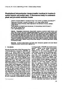
ybrid organic–inorganic all-solid-state solar cells based on methylammonium lead halide perovskite absorbers are currently attracting increasing interest because of their ease of fabrication and performances rivalling the best thin-film photovoltaic devices1–7. Of the various types of perovskites and morphologies reported to date, CH3NH3PbI3 deposited on a mesoporous film of titanium dioxide through a sequential deposition method appears to yield the best certified conversion efficiency1. The optical and electronic properties of perovskite materials have been studied thoroughly in recent decades8–11. As hybrid organic–inorganic lead halide perovskites can cumulate functions of light absorption, n-type conduction6 and p-type conduction12, the current picture for the hybrid spiro-OMeTAD|perovskite|TiO2 cell could be described as follows (Fig. 1). The perovskite absorbs light and electron–hole pairs are created in the material, which can possibly evolve towards the formation of excitons after thermalization of the carriers. Charge separation can then occur through two possible primary reactions: injection of photogenerated electrons into TiO2 nanoparticles (equation (1a)) and/or injection of holes (equation (2a)) into a hole-transporting material (HTM) such as spiroOMeTAD2,13. However, which electron or hole injection process occurs first and, in the latter case, whether electron injection into and transport within the oxide mesoporous film (equation (2b)) is playing any role, remain unclear. The precise role of titanium dioxide in efficient perovskite solar cells based on mesoporous films of this particular metal oxide has indeed not been established clearly. Evidence has been found for electron injection from the mixed halide CH3NH3PbI2Cl into TiO2 (refs 6,14), and the same material has also been reported to yield efficient photovoltaic conversion once dispersed on an insulating alumina framework, in which electron injection is not energetically feasible and where no sensitization of the oxide material can be invoked6.
Electron injection as the primary charge separation step: (e− . . . h+ )perovskite � ecb− (TiO2 ) + h+ (perovskite)
(1a)
h+ (perovskite) � h+ (HTM)
(1b)
Hole injection as the primary charge separation step: (e− . . . h+ )perovskite � h+ (HTM) + e− (perovskite)
(2a)
e− (perovskite) � ecb− (TiO2 )
(2b)
Exciton annihilation: (e− . . . h+ )perovskite � hn′
(3)
(e− . . . h+ )perovskite � ∇
(4)
Back electron transfer at the TiO2 surface: ecb− (TiO2 ) + h+ (perovskite) � ∇
(5)
Back charge transfer at the HTM surface: h+ (HTM) + e− (perovskite) � ∇
(6)
Charge recombination at the TiO2|HTM interface: ecb− (TiO2 ) + h+ (HTM) � ∇
(7)
Undesired reactions such as exciton annihilation, leading to
Photochemical Dynamics Group, Institute of Chemical Sciences and Engineering, E´cole Polytechnique Fe´de´rale de Lausanne, CH-1015 Lausanne, Switzerland, 2 Laboratory for Photonics and Interfaces, Institute of Chemical Sciences and Engineering, E´cole Polytechnique Fe´de´rale de Lausanne, CH-1015 Lausanne, Switzerland, 3 Institute for Solar Fuels, Helmholtz-Zentrum Berlin fu¨r Materialien und Energie GmbH, 14109 Berlin, Germany. * e-mail: je.moser@epfl.ch 1
250
NATURE PHOTONICS | VOL 8 | MARCH 2014 | www.nature.com/naturephotonics
© 2014 Macmillan Publishers Limited. All rights reserved.
NATURE PHOTONICS
ARTICLES
DOI: 10.1038/NPHOTON.2013.374 1.2 e−
(1)
(4)
TiO2
CH3NH3PbI3 TiO2 Al2O3
1.0
(3)
CB
(6)
(7)
0.8
(5) h+
(2)
Spiro OMeTAD
VB
CH3NH3PbI3
Normalized ΔA
E (eV)
CB
CH3NH3PbI3 + spiro TiO2 Al2O3
0.6 0.4 A2
0.2
Figure 1 | Schematic diagram of energy levels and electron transfer processes in an HTM|perovskite|TiO2 cell.
photoluminescence (equation (3)) or to non-radiative recombination (equation (4)), as well as recombination of the charge carriers at the three interfaces (equations (5) to (7)) compete with the extraction of the photogenerated charges. The kinetics of these processes is thus expected to control, to a large extent, the overall photovoltaic conversion efficiency of the system. In this work, we applied time-resolved spectroscopy techniques to assess the individual dynamics of all occurring interfacial photoinduced charge transfer processes and to derive the effective mechanism for charge separation. This information is of paramount importance for understanding the functioning of the devices and eventually for the improvement of their photovoltaic performances. The dynamics of the various charge transfer processes were first assessed by probing optical transient absorption signals in the nearinfrared with CH3NH3PbI3 deposited on either mesoporous TiO2 or Al2O3 films, in the absence of HTM. To support and complement the mechanistic picture of the processes, time-resolved photoconductance measurements were also performed in the microwave frequency range. Because of the mismatch of the energies of the conduction bands of Al2O3 and the perovskite, electron injection is not thermodynamically feasible in this oxide. On alumina and in the absence of HTM, the only possible pathway for energy conservation after light absorption is electron–hole recombination, either through luminescence or non-radiative processes (equations (3) and (4)). Comparison with TiO2 samples thus provides evidence of electron injection (equation (1a)) and subsequent back charge transfer and recombination processes at the TiO2 surface (equations (5) and (7)) once the HTM is introduced into the system. A high power conversion efficiency of the photovoltaic device must obviously imply that the charge recombination processes (equations (3) to (7)) occur on a much slower timescale than the charge separation and extraction processes (equations (1) and (2)). It is therefore of crucial interest to determine the kinetics of these reactions so as to ultimately improve the cell’s performance.
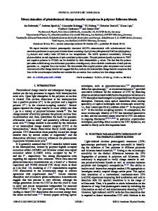
Ultrafast transient optical absorption spectroscopy Femtosecond pump–probe transient absorption experiments were carried out at a probe wavelength of 1.4 mm and an excitation wavelength of 580 nm for CH3NH3PbI3 samples deposited on TiO2 and Al2O3 films, with and without HTM. The resulting transient absorption was found in all cases to rise within the first picosecond (Fig. 2). The decay of the signal traces was observed to be multi-exponential for all samples and was fitted with a double exponential starting at t ¼ 1 ps. The corresponding fast component developed within 40–60 ps for all samples, while a slower component appeared in the 140–270 ps time range. The 1.4 mm probe wavelength was initially selected to probe oxidized spiro-OMeTAD, which absorbs in the near-infrared15,16. However, samples deprived of HTM yielded an important transient absorption signal originating from the perovskite itself. Comparing the signals obtained on the two different metal oxides, it is inferred that they reflect the time evolution of the
0.0 10−12
10−11
10−10
10−9
Time (s)
Figure 2 | Time evolution of electron and hole populations in photoexcited CH3NH3PbI3 perovskite in various systems. Transient absorption signals were measured at a probe wavelength of 1.4 mm following femtosecondlaser pulsed excitation at 580 nm: CH3NH3PbI3 on TiO2 (black); CH3NH3PbI3 on Al2O3 (blue); CH3NH3PbI3 and spiro-OMeTAD on TiO2 (red); CH3NH3PbI3 and spiro-OMeTAD on Al2O3 (green). Thick solid lines represent bi-exponential fits of experimental points starting at t ¼ 1 ps. A2 represents the normalized absorbance change at 25 ps, used as a metric to compare the various samples.
CH3NH3PbI3 photoexcited states population. These excited states correspond to photogenerated electrons and holes, which can either be paired in excitons or exist in the form of free or even trapped charge carriers. In systems prepared on TiO2 films, a small contribution to the transient absorption signal of conduction-band electrons injected in TiO2 cannot be excluded. Similarly, for all systems containing spiro-OMeTAD HTM, contributions to the transient absorption signal of oxidized HTM species cannot be omitted and will be discussed later. In the case of samples without HTM, a transient signal arising from the perovskite deposited on Al2O3 was observed and attributed to the decay of the carriers’ population through recombination within the absorber material (blue trace, Fig. 2) as no interfacial reaction can take place in this case. Transient absorbance of a perovskite|TiO2 sample shows that the relative signal amplitude of the slower part, defined as the normalized absorbance change at 25 ps, is larger than on Al2O3 (Table 1, 24% and 14%, respectively). This relative signal amplitude is subsequently used as a metric to compare the various samples. We will assume in the following discussion that charge recombination within the perovskite is similar on TiO2 and Al2O3 samples. This assumption is corroborated by the observation from transient photoconductance (TPC) measurements (Fig. 3) that the charge decay within the perovskite is not influenced by deposition on a mesoporous framework with respect to perovskite deposited as a flat film on glass. For reasons that will be discussed in the following, the contribution to the transient absorption signal of electrons injected in the TiO2 conduction band is believed to be negligible. From this perspective, the larger
Table 1 | Ratio of amplitude A2 relative to the total normalized amplitude DA0 for CH3NH3PbI3 on TiO2 and Al2O3 , with and without spiro-OMeTAD HTM. A 2/DA 0* TiO2
Without HTM 0.24
With HTM 0.34
Al2O3
0.14
0.26
*A2 measured from data displayed in Fig. 2 at t ¼ 25 ps; DA0 at 1 ps.
NATURE PHOTONICS | VOL 8 | MARCH 2014 | www.nature.com/naturephotonics
© 2014 Macmillan Publishers Limited. All rights reserved.
251
ARTICLES
NATURE PHOTONICS
Time-resolved microwave photoconductance measurements
TPC signal (a.u.)
10−1 CH3NH3PbI3 TiO2 Al2O3 Glass
10−2
10−3
10−4 10−8
10−7
10−6
10−5
10−4
Time (s)
Figure 3 | Transient microwave photoconductance measurements of the perovskite material deposited on various substrates. CH3NH3PbI3 on mesoporous TiO2 (black); CH3NH3PbI3 on mesoporous Al2O3 (blue); CH3NH3PbI3 on flat glass (orange). The build-up rate of the TPC signal is limited here by the excitation laser pulse duration (�10 ns).
relative amplitude for the slower part of the decay observed for the perovskite in contact with TiO2 indicates that some of the charges have already been separated through ultrafast electron injection (equation (1a)). The latter process leaves an excess of holes in the perovskite that take longer to recombine with the remaining electrons, whose population has been depleted. As the decay curves for the TiO2 case begin lagging behind that for Al2O3 at delay times ≥3 ps (Fig. 2, black and blue curves, respectively), it is inferred that charge separation must occur at the perovskite|titania junction on a similar or shorter timescale. Pairs of samples prepared on Al2O3 and TiO2 films were also measured with spiro-OMeTAD impregnating the mesoporous oxides. Interestingly, for a sample of Al2O3 with HTM, the relative amount of remaining charges at a delay time of 25 ps is similar to that observed for the previously discussed sample prepared on TiO2 and without spiro-OMeTAD (Table 1, 26% relative amplitude). This indicates that hole injection into the HTM (equation (2a)) must be completed within a comparable timescale as electron injection into TiO2 (equation (1a)). In the case of perovskite in contact with both TiO2 and the HTM, the amount of longer-lived charges is higher (Table 1, 34% relative amplitude). This result shows that the most efficient charge separation is obtained when using TiO2 and HTM together and is rationalized by the fact that the recombination of the remaining charges in the perovskite must account for charges that are injected at both separate junctions (TiO2|perovskite and perovskite|HTM). Here, in contrast to the case of perovskite deposited on Al2O3 and in contact with the HTM, no residual absorption is observable on the nanosecond timescale, as every carrier in the perovskite should have found an opposite charge with which to recombine. It could be argued that the longlived absorption actually results from the contribution of oxidized spiro-OMeTAD molecules—hþ(HTM)—as well as that of conduction-band electrons in TiO2 , as both species absorb at 1.4 mm (refs 15–17). However, this would not affect the reasoning above, as it would also provide direct evidence of charges having been separated at the junctions. Yet, we believe that these contributions are negligible in our measurements. Indeed, the reactions of ecb2 (TiO2) or hþ(HTM) recombining with carriers in the perovskite (equations (5) and (6)) are likely to take longer than a nanosecond (we show hereafter that the second reaction actually occurs over a microsecond timescale) and thus would appear as a long-lived plateau in the dynamics of the TiO2 þ HTM sample. This is not observed in this case. 252
DOI: 10.1038/NPHOTON.2013.374
As a complementary technique, we used TPC measurements in the microwave frequency range to monitor directly the mobile charge carrier population within the perovskite material. The effect of electron injection from the perovskite into the mesoporous TiO2 and the resulting increase in charge carrier lifetime were observed with a time resolution of 10 ns (Fig. 3). No TPC signal was detected for pure TiO2 or Al2O3 films at the light intensities and excitation wavelength (532 nm) used in these experiments, showing that the observed photoconductance phenomena are induced only by photon absorption in the perovskite. As a result of charge separation or exciton splitting, an increase in the lifetime of the separated charge carriers can normally be observed. For the case with perovskite deposited on Al2O3 without any HTM present, one can expect the degradation of the absorbed photon energy by luminescence or thermalization. This can be clearly seen in Fig. 3, where no significant difference between a pure perovskite film on glass and perovskite deposited on Al2O3 can be observed. In the case where the perovskite is deposited on TiO2 , an extension of the decay time is observed, indicating separation of the electron–hole pair and therefore the injection of electrons into titanium dioxide.
Nanosecond transient optical absorption spectroscopy Flash photolysis experiments were carried out over an extended microsecond-to-millisecond time domain at a probe wavelength of 1.4 mm and an excitation wavelength of 580 nm, similarly to the femtosecond experiments. The expected transient signal in the microsecond timescale results from the absorption of the oxidized form of the spiro-OMeTAD–hþ (HTM)–. Indeed, spectral overlap with charge absorption of the perovskite could be avoided at this wavelength, as the decay of these charges should be completed much earlier within the nanosecond time span. This is confirmed by transient absorption, which shows no signal in the microsecond domain for CH3NH3PbI3 samples without HTM, either on TiO2 or Al2O3 (Fig. 4a). Although we expected to observe a transient signal corresponding to conduction-band electrons in the TiO2 that do absorb at this wavelength, this contribution to the signal appears to be buried in noise in this particular experiment. The time evolution of transient absorbance signals at 1.4 mm for CH3NH3PbI3 samples with HTM (Fig. 4b) on TiO2 and on Al2O3 can, therefore, be assigned to the decay of the oxidized spiroOMeTAD population through recombination processes. On Al2O3 , we observe recombination between hþ (HTM) and e2 (perovskite) (equation (6)), while on TiO2 , recombination occurs between hþ (HTM) and e2 cb (TiO2) (equation (7)). The signal trace decay could be fitted with a stretched exponential (stretching exponent b ¼ 0.5). Excitation energy fluence in this particular experiment being rather low (70 mJ cm22, corresponding to �40 photons per nanoparticle), the stretched exponential reflects a broad distribution of distances between the recombining charges. The difference between the time constants for the decay on TiO2 and Al2O3 is quite evident, and shows that recombination is slower when TiO2 is used (99 ms versus 15 ms on Al2O3). This demonstrates that process (6) is faster than process (7). It therefore provides additional evidence that electron injection has taken place and that recombination occurs via a mechanism that involves diffusion of carriers over a larger distance.
Discussion The intrinsic physical properties of the perovskite material, such as exciton diffusion length, carrier mobility, nature and density of trap states, and the energetics of the bands, are obviously important in explaining why this exceptional material appears to be working in a variety of configurations. Rather than dealing with the intrinsic properties of the perovskite semiconductor, the NATURE PHOTONICS | VOL 8 | MARCH 2014 | www.nature.com/naturephotonics
© 2014 Macmillan Publishers Limited. All rights reserved.
NATURE PHOTONICS a
0.2
ΔA/10−3
0.1
All perovskite-based devices deposited on a mesoporous structure, regardless of preparation type, should fall into one of the two categories (1) or (2). When adding an HTM, these cases can be coupled with two additional cases in relation to the junction:
CH3NH3PbI3 TiO2 Al2O3
0.0 −0.1 −0.2 10−6
10−5
10−4
10−3
Time (s)
b
CH3NH3PbI3 + spiro TiO2 Al2O3
1.0 0.8
Normalized ΔA
ARTICLES
DOI: 10.1038/NPHOTON.2013.374
0.6 0.4 0.2 0.0
10−6
10−5
10−4
10−3
Time (s)
Figure 4 | Charge recombination dynamics obtained from nanosecondlaser flash photolysis of the various systems. Transient absorption signals were monitored at l ¼ 1.4 mm following excitation at 580 nm. a, Samples without HTM: CH3NH3PbI3 on TiO2 (black); CH3NH3PbI3 on Al2O3 (blue). b, Samples with HTM. Signals mainly reflect the decay of the hþ (HTM) population. CH3NH3PbI3 and spiro-OMeTAD on TiO2 (red); CH3NH3PbI3 and spiro-OMeTAD on Al2O3 (green). Thick lines represent stretched exponential fit of data.
present work focuses on interfacial charge transfer processes occurring at the junctions between the light absorber and the electron- and/or hole-conducting materials. A sequence of interfacial electron transfer steps is derived from the kinetics determined experimentally in configurations that have already been proven to function efficiently in solar cells. We can then take for granted that the exciton diffusion length and carrier mobility within the perovskite are easily sufficient and that all energy levels are conveniently aligned18,19. In samples containing the perovskite absorber deposited on a titanium dioxide electron acceptor with HTM infiltrating into the pores of the mesoscopic film, non-ideal morphologies obtained during the preparation will lead to various local situations within the same sample, where perovskite domains could be insulated, in contact with only TiO2 or the HTM, or form two junctions with both the TiO2 and the HTM. All these different scenarios are encountered in current solar energy conversion devices of various architectures. Interest in discussions about the charge transfer mechanism taking place in TiO2|perovskite|spiro-OMeTAD solidstate solar cells therefore extends beyond this particular example to other types of perovskite-based photovoltaic systems. Four different cases related to the morphology of the sample could coexist in perovskite-based devices: (1) All the perovskite is conformally deposited on top of the metal oxide (either the insulating Al2O3 or the TiO2 electron acceptor) as a thin light-harvesting film, with a thickness of at most a few nanometres. (2) Part of the perovskite is not in direct contact with the oxide substrate but is present in the form of isolated crystalline domains in the pores and/or a capping layer on top of the mesoporous network.
(3) All the HTM is conformally deposited into the pores, forming a continuous junction with the perovskite material. (4) Not enough HTM is present in the pores, or the interfacial contact between the perovskite and the HTM is only partial as a result of infiltration problems. We will rationalize, for each case, what could be observed by time-resolved laser spectroscopy, keeping in mind the possible influence of the contact at the various heterojunctions. In case (1), the intimate contact between the two semiconductors allows the electron injection process to be resolved unequivocally by a direct comparison between TiO2- and Al2O3-based samples. In case (2), a capping layer of perovskite that is not in direct contact with the mesoporous oxide can be found and optical features of isolated perovskite material could be observed. In the specific case of TiO2 , where we expect electron injection to take place, the presence of a capping layer would result in strong light absorption within this layer and consequently poor quenching by TiO2 due to lack of a good TiO2|perovskite interface. Consequently, strong photoluminescence will be observed. In the absence of a good intimate contact with TiO2 , the device can still work, with the perovskite playing the role of the electron-transporting material, as in the so-called meso-superstructured cells built on an insulating Al2O3 framework6. In case (3), a hole is easily extracted at the perovskite|HTM interface, according to measurements already reported5, where the spiro-OMeTAD was shown to very efficiently quench perovskite’s photoluminescence within a sub-picosecond time frame. In case (4), the absence of intimate contact between the light absorber and spiro-OMeTAD is likely to lead to a situation where the device resembles a p-type perovskite cell, where the CH3NH3PbI3 works as the hole-transporting material12. For a perovskite|HTM bilayer, in which holes have to diffuse across a 65-nm-thick absorber layer to reach the HTM junction, the extraction time extends to the picosecond-to-nanosecond timescale, much longer than for case (3)19. Case (4) will often occur in type (2) samples, because a capping layer of perovskite tends to prevent good infiltration of the HTM into the pores. Deposition of spiroOMeTAD on a case (1) sample will, in contrast, favour case (3), resulting in an optimal device1. Part of the charge recombination observed in TiO2|perovskite|spiro-OMeTAD samples can still occur from electrons in the perovskite (equation (6)) if they have not been injected efficiently into the TiO2. This would be the case if there were insufficient contact between the TiO2 and the perovskite—case (2). The time constant measured by flash photolysis experiments for a TiO2 þ HTM sample thus might include contributions from the recombination reactions (equations (6) and (7)). The time-resolved measurements reported in the present work highlight, for the first time, some of the important processes in CH3NH3PbI3-sensitized samples and corresponding samples built on an Al2O3 scaffold. Probing in the near-infrared provides a way to circumvent spectral overlap arising from different types of morphological issue—case (1) or (2)—by observing only the carriers’ population decay inside the perovskite itself rather than in the bulk luminescence that constitutes the main spectral feature observed in the visible range. In previous work by Kim and colleagues5, electron injection could not be demonstrated by monitoring the stimulated emission of the perovskite, most likely because the observed transient was originating from a capping layer of the material. The method originally used in this work to produce the samples consisted in spin-coating a mixed solution of CH3NH3I
NATURE PHOTONICS | VOL 8 | MARCH 2014 | www.nature.com/naturephotonics
© 2014 Macmillan Publishers Limited. All rights reserved.
253
ARTICLES
NATURE PHOTONICS
and PbI2 in gamma-butyrolactone5. This has now been replaced by a sequential deposition method yielding more conformal films1. Near-infrared optical probing, which monitors the decay of the population of charges remaining in the photoexcited perovskite, is key in demonstrating charge separation processes taking place through both electron and hole injection. Comparable kinetics for the decay of the remaining recombining charges in the perovskite|TiO2 and spiro-OMeTAD|perovskite|Al2O3 samples indicate that electron and hole injection occur on similar timescales. Furthermore, it is possible to conclude that both charge separation processes happen on a femtosecond-to-picosecond timescale, as our previous study showed that hole injection, observed through stimulated emission quenching, has already taken place within the first picosecond following excitation5. Direct monitoring of the dynamics of primary charge separation is beyond the scope of this study. The efficiency of charge extraction in a perovskite solar cell depends on the ratio between the rate constants for charge recombination and charge separation. It is thus important to determine the timescale for charge recombination processes in the cell. Results obtained by flash photolysis show that the recombination reaction for electrons and oxidized spiro-OMeTAD (equations (6) and (7)) is slow, taking place in the microsecond range. This indicates a factor of at least 106 between charge separation and recombination rate constants at the HTM interface, ensuring a quantitative yield for sustained charge separation. Additionally, reaction (7), being slower than reaction (6), proves that the use of TiO2 as electron acceptor and transporter in conjunction with an organic HTM in contact with the perovskite is indeed quite beneficial.
Conclusion Time-resolved techniques were applied to CH3NH3PbI3 deposited as a conformal film on TiO2 and Al2O3 samples to study the kinetics of interfacial electron transfer processes. Using ultrafast spectroscopy in the near-infrared, we were able to monitor transient absorption by photogenerated charges in the perovskite. The results showed that the decay of the charge population is delayed upon infiltration with the hole-transporting material spiroOMeTAD, which is consistent with previous evidence of primary hole injection from the photoexcited perovskite into the HTM. Moreover, evidence for electron injection from CH3NH3PbI3 into the TiO2 film was found. The latter process appears to occur over a similar timescale as hole injection. Further evidence was provided by TPC measurements, with a slower charge decay in the presence of TiO2 found in the microwave frequency range. Additionally, transient absorbance decay of oxidized spiroOMeTAD was monitored in the near-infrared. Experimental data showed that charge recombination with oxidized HTM species, which occurs over a microsecond timescale, is delayed on TiO2 films with respect to Al2O3 , indicating that the mechanism involves recombination of charges separated by a longer distance. The observation of charge separation and charge recombination reactions is closely related to the method of preparing the samples. Optical signals can be largely influenced by the presence of a capping layer of perovskite that is not conformally deposited on the mesoporous oxide film. Conformal coating of the TiO2 surface with CH3NH3PbI3 facilitates charge separation by ensuring direct electron injection into the oxide. These findings highlight the advantage of employing two heterojunctions with titanium dioxide and the HTM while using perovskite as a solid-state light absorber.
Methods Sample preparation. For the preparation of substrate films, TiO2 and Al2O3 pastes were chosen that had porosities and particle sizes as similar to each other as possible. A commercial TiO2 paste (Dyesol 18 NR-T, 18 nm average nanoparticle diameter) 254
DOI: 10.1038/NPHOTON.2013.374
was used, diluted 1:3 (wt) in EtOH, yielding mesoporous films with an average pore size of 24 nm. A home-made Al2O3 paste (17 nm average nanoparticle diameter) was used diluted 1:3 (wt) in EtOH, yielding films with an average pore size of 32 nm. The TiO2 and Al2O3 pastes (100 ml) were spin-coated on 2 × 2 cm glass microscope slides (5,000 r.p.m.,1,000 r.p.m. s21, 30 s). The films were then dried for 15 min at 100 8C and sintered for 30 min at 500 8C. These conditions yielded an average thickness of 400 nm for the TiO2 and 270 nm for the Al2O3 films, as measured by atomic force microscopy (Asylum Research Chypher). PbI2 (99%, Sigma-Aldrich) was dissolved in dimethylformamide at 70 8C to yield a concentration of 1 M. The PbI2 solution (100 ml) was spin-coated on the mesoporous substrates (6,500 r.p.m., 5,500 r.p.m. s21, 30 s). The films were then dried for 15 min at 70 8C. Methylammonium iodide was synthesized according to a reported procedure7 and a solution of 20 mg ml21 of CH3NH3I in isopropanol was prepared. PbI2 substrates were immersed in this solution for 1 min 40 s, leading to a drastic colour change of the film from yellow to dark brown. The films were rinsed in isopropanol for 10 s. A solution of spiro-OMeTAD (Merck KGaA) was prepared by dissolving 90 mg in 1 ml chlorobenzene at 60 8C. 4-Tert-butylpyridine (tBP, Sigma-Aldrich; 8.75 ml) was added to the latter chlorobenzene solution to yield a concentration of 0.06 M tBP. Lithium bis(trifluoromethylsulphonyl)imide (LiTFSI, Sigma-Aldrich; 17 mg) was predissolved in 100 ml acetonitrile, and 18.75 ml of this solution was added to the same chlorobenzene solution to yield a concentration of 0.011 M LiTFSI. The spiro-OMeTAD solution (80 ml) with tBP and LiTFSI added was deposited onto the perovskite films and allowed to infiltrate for 10 s to maximize the penetration of the HTM before spin-coating (4,000 r.p.m., 770 r.p.m. s21, 30 s). All spin-coating operations were carried out in a dry glovebox under an argon atmosphere. After preparation, samples were placed under vacuum for a few minutes, stored in the glovebox, and finally encased in a sealed cell containing argon to avoid contact with air and oxygen during measurements. Nanosecond flash photolysis. Transmission-mode transient absorption spectroscopy experiments were conducted using a frequency-tripled, Q-switched Nd:YAG laser (Continuum, 20 Hz repetition rate) pumping an optical parametric oscillator (OPO-355, GWU). The output wavelength of the OPO was tuned at lexc ¼ 580 nm (7 ns pulse duration) and attenuated to 70 mJ cm22. The continuous-wave probe light from a xenon arc lamp was passed through various optical elements, the sample and a monochromator (lprobe ¼ 1.4 mm) before being detected by an InGaAs photodiode with 1 kV load (SM05PD5A, Thorlabs). Averaging over at least 2,000 laser shots was carried out. Dynamics were recorded over 10,000 points and a second-order Savitzky–Golay smoothing algorithm on 45 points was applied. Femtosecond laser spectroscopy. Transient absorption spectra were recorded using femtosecond pump–probe spectroscopy. The pump beam (lexc ¼ 580 nm) was generated by pumping a two-stage non-collinear optical parametric amplifier (NOPA) by the 778 nm output of an amplified Ti:sapphire laser system (ClarkMXR, CPA-2001), providing 150 fs pulses at a repetition rate of 1 kHz. The probe beam (lprobe ¼ 1.4 mm) was generated by a second OPA (Light Conversion, TOPAS model 4/800) and used without any compression (pulse duration �150 fs). The change in transmittance of the sample, that is, the change in intensity of the probe beam, was measured by an InGaAs photodiode (New Focus, model Nirvana 2017) protected by cutoff filters to avoid any scattered light from the pump. The lowamplitude signal was extracted by a lock-in amplifier (SR-830, Stanford Research) referenced to the chopper. The pump energy at the sample was 360 nJ/pulse with a spot size diameter of �560 mm. Temporal overlap between the pump and probe pulses at the sample position was measured with a Kerr gating technique and gave a typical instrument response function of 180 fs. Time-resolved microwave conductivity measurements. TPC measurements in the microwave frequency range were performed by using a Ka-band (28.5–40 GHz) apparatus, as described previously20. Samples were excited by 10 ns (full-width at half-maximum) pulses of a frequency-doubled Q-switched Nd:YAG laser at a wavelength of 532 nm with a beam diameter of �1.6 mm. The excitation intensity was adjusted by the use of calibrated filters and set to 1,200 mJ cm22 for samples on mesoporous films, while 7 mJ cm22 was used for samples deposited on glass, which contained more perovskite material.
Received 13 July 2013; accepted 17 December 2013; published online 19 January 2014
References 1. Burschka, J. et al. Sequential deposition as a route to high-performance perovskite-sensitized solar cells. Nature 499, 316–319 (2013). 2. Heo, J. H. et al. Efficient inorganic–organic hybrid heterojunction solar cells containing perovskite compound and polymeric hole conductors. Nature Photon. 7, 486–491 (2013). 3. Noh, J. H., Im, S. H., Heo, J. H., Mandal, T. N. & Seok, S. I. Chemical management for colorful, efficient, and stable inorganic–organic hybrid nanostructured solar cells. Nano Lett. 13, 1764–1769 (2013). NATURE PHOTONICS | VOL 8 | MARCH 2014 | www.nature.com/naturephotonics
© 2014 Macmillan Publishers Limited. All rights reserved.
NATURE PHOTONICS
ARTICLES
DOI: 10.1038/NPHOTON.2013.374
4. Qiu, J. et al. All-solid-state hybrid solar cells based on a new organometal halide perovskite sensitizer and one-dimensional TiO2 nanowire arrays. Nanoscale 5, 3245–3248 (2013). 5. Kim, H.-S. et al. Lead iodide perovskite sensitized all-solid-state submicron thin film mesoscopic solar cell with efficiency exceeding 9%. Sci. Rep. 2, 591 (2012). 6. Lee, M. M., Teuscher, J., Miyasaka, T., Murakami, T. N. & Snaith, H. J. Efficient hybrid solar cells based on meso-superstructured organometal halide perovskites. Science 338, 643–647 (2012). 7. Im, J.-H., Lee, C.-R., Lee, J.-W., Park, S.-W. & Park, N.-G. 6.5% efficient perovskite quantum-dot-sensitized solar cell. Nanoscale 3, 4088–4093 (2011). 8. Papavassiliou, G. C. Three- and low-dimensional inorganic semiconductors. Prog. Solid State Chem. 25, 125–270 (1997). 9. Ishihara, T. Optical properties of PbI-based perovskite structures. J. Lumin. 60, 269–274 (1994). 10. Mitzi, D. B. Templating and structural engineering in organic–inorganic perovskites. J. Chem. Soc. Dalton Trans. 1–12 (2001). 11. Stoumpos, C. C., Malliakas, C. D. & Kanatzidis, M. G. Semiconducting tin and lead iodide perovskites with organic cations: phase transitions, high mobilities, and near-infrared photoluminescent properties. Inorg. Chem. 52, 9019–9038 (2013). 12. Etgar, L. et al. Mesoscopic CH3NH3PbI3/TiO2 heterojunction solar cells. J. Am. Chem. Soc. 134, 17396–17399 (2012). 13. Bi, D., Yang, L., Boschloo, G., Hagfeldt, A. & Johansson, E. M. J. Effect of different hole transport materials on recombination in CH3NH3PbI3 perovskitesensitized mesoscopic solar cells. J. Phys. Chem. Lett. 4, 1532–1536 (2013). 14. Liu, M., Johnston, M. B. & Snaith, H. J. Efficient planar heterojunction perovskite solar cells by vapour deposition. Nature 501, 395–398 (2013). 15. Snaith, H. J. et al. Charge collection and pore filling in solid-state dye-sensitized solar cells. Nanotechnology 19, 424003 (2008). 16. Olson, C., Veldman, D., Bakker, K. & Lenzmann, F. Characterization of the pore filling of solid state dye sensitized solar cells with photoinduced absorption spectroscopy. Int. J. Photoenergy 2011, 513089 (2011). 17. Rothenberger, G., Fitzmaurice, D. & Gra¨tzel, M. Spectroscopy of conduction band electrons in transparent metal oxide semiconductor films: optical determination of the flatband potential of colloidal titanium dioxide films. J. Phys. Chem. 96, 5983–5986 (1992).
18. Stranks, S. D. et al. Electron–hole diffusion lengths exceeding 1 micrometer in an organometal trihalide perovskite absorber. Science 342, 341–344 (2013). 19. Xing, G. et al. Long-range balanced electron- and hole-transport lengths in organic–inorganic CH3NH3PbI3. Science 342, 344–347 (2013). 20. Friedrich, D. & Kunst, M. Analysis of charge carrier kinetics in nanoporous systems by time resolved photoconductance measurements. J. Phys. Chem. C 115, 16657–16663 (2011).
Acknowledgements Financial support was provided by the Swiss National Science Foundation and the NCCRMUST programme. M.G. and J.T. acknowledge the European Research Council (ERC) for an Advanced Research Grant (ARG no. 247404) funded under the ‘Mesolight’ project. A.M. and J.-E.M. thank J. Burschka, A. Dualeh, S. M. Zakeeruddin and C. Gra¨tzel for discussions, P. Comte for the preparation of Al2O3 paste, P. Gao for the preparation of CH3NH3I, A. Devizˇis for help with near-infrared detection and A. Gasperini for atomic force microscopy measurements.
Author contributions A.M. designed the experiments and prepared the samples. A.M. and J.T. carried out the laser experiments and analysed the data with J.-E.M. T.M. and D.F. designed the photoconductance experiments. D.F. performed the microwave experiments on the samples prepared by T.M. and analysed the data with the help of T.M., M.K. and R.vdK. A.M. prepared the manuscript with the help of J.T. and J.-E.M. J.-E.M. designed the femtosecond and nanosecond experimental spectroscopy tools, conceived the project and directed the work. All other authors discussed the results and commented on the manuscript.
Additional information Reprints and permissions information is available online at www.nature.com/reprints. Correspondence and requests for materials should be addressed to J.-E.M.
Competing financial interests The authors declare no competing financial interests.
NATURE PHOTONICS | VOL 8 | MARCH 2014 | www.nature.com/naturephotonics
© 2014 Macmillan Publishers Limited. All rights reserved.
255