APPLIED PHYSICS LETTERS
VOLUME 75, NUMBER 17
25 OCTOBER 1999
Quantum interference control of currents in CdSe with a single optical beam N. Laman,a) A. I. Shkrebtii, J. E. Sipe, and H. M. van Driel Department of Physics, University of Toronto, Toronto, Canada M5S 1A7
共Received 21 June 1999; accepted for publication 24 August 1999兲 We show that ballistic current generation can occur in a semiconductor via quantum interference between absorption pathways for orthogonal polarization components of a single-frequency beam. This effect occurs for a subset of noncentrosymmetric materials, is macroscopically associated with a second-order nonlinear optical susceptibility, and produces current injection linearly proportional to the beam intensity. We demonstrate this in wurtzite CdSe (E g ⫽1.75 eV) at 295 K using cw and femtosecond optical sources of wavelength 600–750 nm 共2.07–1.66 eV兲. The intensity and spectral dependence are in reasonable agreement with a first-principles calculation. Continuous current density of 30 A cm⫺2 is produced for 60 mW cm⫺2 intensity at 633 nm. © 1999 American Institute of Physics. 关S0003-6951共99兲00843-8兴
The use of quantum interference to control the properties of semiconductors via phased optical beams has been a subject of growing interest in recent years.1–6 Previously, our group has shown that interference between one- and twophoton absorption amplitudes, for beams of frequency and 2 with ប ⬍E g ⬍2ប , can inject current in bulk, crystalline semiconductors of band gap E g . The magnitude and direction of the current can be controlled by adjusting the beams’ relative phase. In the context of macroscopic nonlinear optics, the current injection process can be related to a physically divergent component of Im 3(⌺ ;,,⫺2 ⫺⌺) as ⌺ →0.7 Since this phenomenon is based on a fourth-rank tensor, it can occur in centro- and noncentrosymmetric materials. An obvious question arises: Can current be injected and coherently controlled via a lower-order nonlinear process? Here, we show that for a subset of noncentrosymmetric crystals, current injection can indeed occur via quantum interference of absorption processes involving orthogonally polarized components of a single color beam, at frequency , for ប ⬎E g . Related processes involving anisotropic carrier scattering and photovoltaic effects in doped and undoped materials have been previously discussed phenomenologically8 under the name of ‘‘circular photocurrent.’’ However, the connection to nonlinear optics and coherence control was not made. We do so here for processes involving band–band absorption. In considering how a single beam with electric field E(t)⫽E( )exp(⫺it)⫹c.c. can inject an electron 共e兲 or hole 共h兲 current density (Je,h ), phenomenologically,9 the lowestorder process must be of the form i dJ e,h
dt
i jk ⫽ e,h 共 兲 E j 共 兲 E k 共 ⫺ 兲 ⫹c.c.,
共1兲
we used both a simple Fermi’s Golden Rule calculation3 and the general nonlinear susceptibility formalism9–11 within an independent particle approximation. Both calculations yield the result
iejk 共 兲 ⫽
a兲
Electronic mail:
[email protected]
i v cc 共 k兲 兵 r cj v 共 k兲 r kv c 共 k兲 兺 cvk
⫺r kc v 共 k兲 r vj c 共 k兲 其 ␦ „ c v 共 k兲 ⫺ …,
共2兲
where the subscripts c and v refer to conduction and valence bands, rnm (k) is the interband matrix element of the position operator, and V is the normalization volume of the crystal. The tensor ihjk ( ) is found by replacing the velocity matrix i (k) with ⫺ v ivv (k). element v cc i jk ( ), based on time-reversal From the expression for e,h i jk i jk ( )…* ⫽⫺ e,h ( ), i.e., symmetry one can show that „ e,h i jk ik j i jk e,h ( ) is purely imaginary, and e,h ( )⫽⫺ e,h ( ). 7,11 for a cold, clean Within the context of nonlinear optics, semiconductor and neglecting relaxation effects, 2 (⫺ ⌺ ; ⫹ ⌺ ,⫺ )→ e,h ( )/(⫺i ⌺ ) 2 ⫹¯ as ⌺ →0; i.e., the single-beam coherent control process is similar to the two-beam process in that it is also related to a doubly divergent piece of a nonlinear susceptibility. The calculation of e,h ( ) from Fermi’s Golden Rule makes the physics of this current injection clear: It arises from the interference of two one-photon absorption processes corresponding to orthogonal polarizations of the incident light, as indicated in Fig. 1共a兲. Since e,h is purely imaginary, Eq. 共1兲 can be written i dJ e,h
dt
i jk ⫽⫺2„Im e,h 共 兲 …兩 E j 共 兲 兩兩 E k 共 兲 兩 sin共 j ⫺ k 兲 ,
共3兲
where E ( )⫽ 兩 E ( ) 兩 exp(i ), etc. It is clear that only elliptically polarized beams will induce current flow, and that right- and left-circularly polarized light will inject current in opposite directions. Relaxation effects neglected in Eq. 共3兲 can be included phenomenologically by adding a term i / e,h to the right-hand side, where e,h represents the ⫺J e,h current 共intraband兲 momentum relaxation time for electrons j
where the superscripts are Cartesian components and are summed over when repeated; is taken to be positive and the fields are evaluated inside the medium. To derive the i jk ( ) from the microscopic transition amplitudes tensor e,h
e3 1 2ប 2 V
j
j
0003-6951/99/75(17)/2581/3/$15.00 2581 © 1999 American Institute of Physics Downloaded 21 Aug 2006 to 128.100.75.55. Redistribution subject to AIP license or copyright, see http://apl.aip.org/apl/copyright.jsp
2582
Appl. Phys. Lett., Vol. 75, No. 17, 25 October 1999
Laman et al.
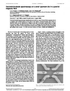
FIG. 1. 共a兲 Schematic diagram of single-beam interference via band–band absorption involving different polarization components; 共b兲 experimental configuration used for current generation in CdSe.
and holes. The total current is J⫽Je ⫹Jh , and the total current injection tensor can be written ⫽ e ⫹ h . Since e,h is a third-rank tensor, it is nonzero only in materials without center-of-inversion symmetry. Of the 32 crystal classes, 21 lack center-of-inversion symmetry. But, since e,h is antisymmetric in its last two Cartesian indices, it only survives for 18 of the crystal classes.12 Unfortunately, bulk zinc-blende semiconductors such as GaAs belong to one of the crystal classes for which e,h vanishes. Nonetheless, e,h is nonzero for the wurtzite structure, into which many of the II–VI semiconductors crystallize. One of these, CdSe, is commercially available and with E g ⫽1.75 eV can be used with visible light sources. We make use of the nony yz ( ) element, where z is taken parallel to the hexzero e,h agonal axis. Current then can be collected along the y direction using a configuration as shown in Fig. 1共b兲. Unlike two-beam coherent control,3 where balance of single- and two-photon absorption rates can optimize interference process with nearly all the carriers moving in one direction, in the one-beam process the independent (y,z) absorption rates and their interference are both proportional to intensity I , so that the efficacy is intensity independent but may depend on . The carrier distribution asymmetry in momentum space is related to intrinsic crystal properties, in this case, how ‘‘noncentrosymmetric’’ the crystal is. For CdSe the efficacy is estimated to be 10%; i.e., the maximum current is 10% of the value obtained if all injected carriers were traveling in one direction with their injected speed 共for the electrons, this speed is ⬃100 km s⫺1 for ប ⫽2.0 eV兲. However, unlike the two-beam process the injected ballistic current scales with the intensity of the incident light. This, along with the large size of y yz ( ) 共⬃5⫻108 A V⫺2 s⫺1 at 630 nm兲, and for13 e,h ⫽4⫻10⫺14 s, gives a steady-state 共J ⬃2 A cm⫺2 for intensity I⫽1 mW cm⫺2兲 meaning that
FIG. 2. 共a兲 Phase dependent current in CdSe generated with a 0.63 m beam with polarization state indicated. 共b兲 Variation of current signal with intensity.
currents can be observed using a low-power continuouswave source. The experimental configuration we used to demonstrate single-beam current injection at 295 K is given in Fig. 1共b兲. A single crystal of high resistivity CdSe (10 mm⫻10 mm ⫻1 mm) had deposited silver electrodes placed 1.3 mm apart with the hexagonal axis located in the plane of the face and perpendicular to the gap direction. Light from a 3 mW, 0.63 m 共1.96 eV兲 He–Ne laser was passed through a variable attenuator and focused at normal incidence onto the CdSe to generate current across the gap 共parallel to the crystal y axis兲. A Soleil–Babinet compensator was used to control the polarization state. The current can be injected into the electrodes by illuminating the entire gap or it can induce charges on the electrodes by illuminating only a region of the sample within the gap 共voltage injection associated with charge separation兲; for the same incident power the induced voltage is, typically, 3–5 times smaller in the latter case. For insidegap illumination, the induced steady-state voltage (V) measured as a function of ( y ⫺ z ), 14 with a lock-in amplifier, is shown in Fig. 2共a兲15. The current has maximum amplitude for circular polarization but changes direction for right and left states, as expected. As Fig. 2共b兲 shows, the steady-state voltage varies as V⬀I 0.78. The departure from linearity may be related to several factors such as a non-Ohmic electrode response and trap dynamics during steady excitation. Also, the experiments measure the steady-state cumulative charge and not dJ/dt directly. We have determined the magnitude of by illuminating the entire gap and treating the sample as a leaky capacitor under steady state. With an average intensity of 60 mW cm⫺2 along the electrode edge, we measure a voltage modulation amplitude of 110 V. From the knowl-
Downloaded 21 Aug 2006 to 128.100.75.55. Redistribution subject to AIP license or copyright, see http://apl.aip.org/apl/copyright.jsp
Laman et al.
Appl. Phys. Lett., Vol. 75, No. 17, 25 October 1999
2583
ages should not be compared to the cw voltages, since both the circuit dynamics and microscopic current behave differently on the different time scales. In summary, we have demonstrated a single-beam technique for coherently generating and controlling current flow in semiconductors in the absence of a dc electrical bias. The current amplitude varies nearly linearly with beam intensity, indicating possible applications in polarization-controlled devices. The magnitude and spectral dependence of the current response are in reasonable agreement with a first-principles calculation after corrections for charge collection geometry are considered. FIG. 3. Calculated spectral dependence of y yz in CdSe. The data represent the spectral dependence of current injection using a 130 fs optical parametric amplifier; the vertical scales have been chosen to yield a common peak amplitude.
edge of the absorption coefficient16 (5.5⫻104 cm⫺1), the resistance of the illuminated area, 2.0 M⍀, and the illuminated electrode length, 1.1 mm, we calculate a current density of J⫽30 A cm⫺2. This translates into y yz ⬇1 8 ⫺2 ⫺1 ⫻10 A V s as compared with a theoretical value17 of 5⫻108 A V⫺2 s⫺1. Given the nature of the experiments and calculations, we regard the agreement as good. We anticipate that part of any discrepancy is due to lack of exact knowledge of charging and discharge dynamics, including electrode collection efficiency; for the deposited electrodes, it is possible that not all directed charge produced within the absorption depth is collected. Note, however, that the current generated per carrier created is substantial. To determine the spectral response of the current injection process we used a 250 kHz repetition rate, 130 fs source tunable from 600 to 750 nm 共2.07–1.66 eV兲.3 Figure 3 shows the induced steady-state voltage as a function of photon energy at constant photon flux 共corresponding to an average intensity of 14 mW/cm2 at 700 nm兲. Also illustrated is the calculated dependence of y yz ( ) vs .17 As expected, both experimentally and theoretically, y yz ( ) increases away from the threshold for band–band absorption; the peak is related to the fact that the threshold for valence-band ionization is largest when the associated continuum state wave functions have their largest overlap. This occurs just above the threshold for ionization. The comparison of the theoretical y yz ( ) with the experimental 共voltage兲 spectral profiles is good except at the highest photon energies. As with the magnitude of the response, the discrepancy may reflect that the experiment does not measure y yz ( ) directly but may also reflect electrode effects and the variation of the absorption depth with photon energy. The magnitude of these volt-
The authors gratefully acknowledge financial support from the Natural Sciences and Research Council of Canada and Photonics Research Ontario. Technical support from J. Fraser and S. Grabtchak and helpful discussions with A. Shik are gratefully acknowledged.
1
R. Atanasov, A. Hache´, J. L. P. Hughes, H. M. van Driel, and J. E. Sipe, Phys. Rev. Lett. 76, 1703 共1996兲. 2 A. Hache´, Y. Kostoulas, R. Atanasov, J. L. P. Hughes, J. E. Sipe, and H. M. van Driel, Phys. Rev. Lett. 78, 306 共1997兲. 3 A. Hache´, J. E. Sipe, and H. M. van Driel, IEEE J. Quantum Electron. 35, 1144 共1998兲. 4 E. Dupont, P. B. Corkum, H. C. Liu, M. Buchanan, and Z. R. Wasilewsky, Phys. Rev. Lett. 74, 3596 共1995兲. 5 J. J. Baumberg, A. P. Heberle, K. Ko¨hler, and K. H. Ploog, J. Opt. Soc. Am. B 13, 1246 共1996兲. 6 N. H. Bonadeo, J. Erland, D. Gammon, and D. G. Steel, Science 282, 1473 共1998兲. 7 C. Aversa and J. E. Sipe, IEEE J. Quantum Electron. 32, 1570 共1996兲. 8 B. I. Sturman and V. M. Fridkin, The Photovoltaic and Photorefractive Effects in Noncentrosymmetric Materials 共Gordon and Breach, Philadelphia, PA, 1992兲. 9 J. E. Sipe and A. I. Shkrebtii 共unpublished兲. 10 J. E. Sipe and E. Ghahramani, Phys. Rev. B 48, 11705 共1993兲. 11 C. Aversa and J. E. Sipe, Phys. Rev. B 52, 14636 共1995兲. 12 See, for example, E. G. Sauter, Nonlinear Optics 共Wiley, New York, 1996兲. 13 O. Madelung, Semiconductors—Basic Data, 2nd ed. 共Springer, Berlin, 1996兲, p. 185. 14 Because CdSe is birefringent in the configuration used, this phase difference will change as an arbitrarily polarized beam enters the crystal. However, since the absorption depth 共which is also slightly polarization sensitive兲 is much less than the coherence length c/ 兩 n y ⫺n z 兩 ⫺1 , the phase change is small 关Palik, Handbook of Optical Constants of Solids II 共Academic, San Diego, CA, 1991兲, p. 570兴. For ប ⫽2.0 eV the values are 0.2 and 6 m, respectively. 15 Typically, a phase-independent background signal is also induced with a magnitude between a few % and 100% of that of the modulated signal depending on the Ohmic quality of the electrodes. 16 Palik, Handbook of Optical Constants of Solids II 共Academic, San Diego, CA, 1991兲, p. 570. 17 This is carried out at the FLAPW (DFT-LDA⫹scissors) approximation; R. Atanasov, A. Hache´, J. L. P. Hughes, H. M. van Driel, and J. E. Sipe, Phys. Rev. Lett. 76, 1703 共1996兲.
Downloaded 21 Aug 2006 to 128.100.75.55. Redistribution subject to AIP license or copyright, see http://apl.aip.org/apl/copyright.jsp