Utilizing Electrical Characteristics of Individual Nanotube Devices to Study the Charge Transfer between CdSe Quantum Dots and Double-Walled Nanotubes Yuqi Zhu,*,† Ruiping Zhou,† Lei Wang,‡ Stanislaus S. Wong,‡,§ and Joerg Appenzeller† †
Department of Electrical and Computer Engineering and Birck Nanotechnology Center, Purdue University, West Lafayette, Indiana 47907, United States ‡ Department of Chemistry, State University of New York at Stony Brook, Stony Brook, New York 11794-3400, United States § Condensed Matter Physics and Materials Science Division, Brookhaven National Laboratory, Building 480, Upton, New York 11973, United States S Supporting Information *
ABSTRACT: To study the charge transfer between cadmium selenide (CdSe) quantum dots (QDs) and double-walled nanotubes (DWNTs), various sizes of CdSe−ligand−DWNT structures are synthesized, and fieldeffect transistors from individual functionalized DWNTs rather than networks of the same are fabricated. From the electrical measurements, two distinct electron transfer mechanisms from the QD system to the nanotube are identified. By the formation of the CdSe−ligand−DWNT heterostructure, an effectively n-doped nanotube is created due to the smaller work function of CdSe as compared with that of the nanotube. In addition, once the QD−DWNT system is exposed to laser light, further electron transfer from the QD through the ligand, that is, 4-mercaptophenol (MTH), to the nanotube occurs and a clear QD size-dependent tunneling process is observed. The detailed analysis of a large set of devices and the particular methodology employed here for the first time allowed for extracting a wavelength and quantum dot size-dependent charge transfer efficiencya quantity that is evaluated for the first time through electrical measurement. izing individual decorated double-wall carbon nanotubes (DWNTs) allows for a previously unachievable quantitative analysis of the charge transfer between QDs and the nanotube channel. In fact, all of the above references had focused on the qualitative demonstration of a photoresponse, which only17 determined the amount of charge transfer to some extent quantitatively for a particular CdSe−ligand−SWNT network under one laser wavelength. Here, we present for the first time a comprehensive analysis of the impact of QD size and laser wavelength, which resulted in the extraction of the charge transfer efficiency ke, a quantity that had not been considered previously at the nanoscale. The key differences between our devices and those previously published are (1) the absence of tunneling resistance between tubes that typically obscures the current contributions from transport inside of the individual tubes in a nanotube
Semiconducting quantum dots (QDs) exhibit strongly sizedependent optical and electronic properties due to their tunable band gaps1−3 and are frequently employed as key ingredients for solar cell and photodetector applications.4−9 On the other hand, semiconducting carbon nanotubes (CNTs) have demonstrated outstanding electrical transport properties, giving rise to field-effect transistors with performance specifications that are unrivaled by other materials10,11 and excellent switching behavior with large gate-induced on/off current ratios.10−13 Combining these two interesting and distinctive materials together is believed to potentially result in a heterostructure with attributes for solar cell applications beyond the conventionally achievable performance specs.14,15 However, for low-dimensional materials and combinations of the same, the key to designing desired electronic properties is a detailed understanding of all interfaces involved and, in the context of a QD−CNT system, charge transfer through the same interfaces. While previous studies have focused on QD-decorated nanotube networks, in particular, derived from single-wall carbon nanotubes (SWNTs),16−19 our approach of character© XXXX American Chemical Society
Received: January 9, 2017 Accepted: February 24, 2017 Published: February 24, 2017 717
DOI: 10.1021/acsenergylett.7b00023 ACS Energy Lett. 2017, 2, 717−725
Letter
http://pubs.acs.org/journal/aelccp
Letter
ACS Energy Letters
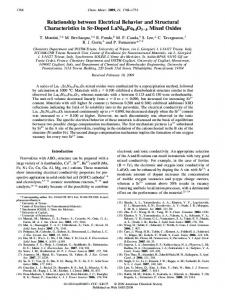
Figure 1. (A) TEM image of DWNT−MTH−CdSe heterostructure with 3.0 nm QDs. (B) AFM image of our farbicated device with individual DWNT−MTH−CdSe. (C) Zoom-in view of (1B); QDs are visible on the surface of the DWNT. (D) AFM scan confirms that the QD height is about 3 nm and that the DWNT diameter is about 2.5 nm.
network, (2) the easy access to so-called ambipolar device characteristics, that is, electron transport for positive and hole transport for negative gate voltages, a particular feature and advantage of our approach that allows determination of the amount of charges transferred from one system component to the other, which is not possible in so-called unipolar devices, as previously reported,16−19 and (3) the use of DWNTs rather than SWNTs, which allows for the chemical modification of the outer shell without impacting the electronic signature of the inner shell, thereby leaving an unperturbed nanotube available for carrier transport. 4-Mercaptophenol (MTH) with the terminal thiol−SH is chosen as the linker molecule (ligand) due to its strong affinity for CdSe and favorable π−π interactions with CNTs through which the heterostructure is formed. In this context, it is worth noting that MTH is known to act as a “hole-scavenger”,20,21 which prevents hole transfer from occurring between the QDs and the nanotube, an aspect that will be discussed in greater detail below. The challenge in using individual DWNTs lies in a rather large variation of DWNT device characteristics, which obviously has to be controlled to ensure a meaningful interpretation of I−V measurements. Two main sources for these variations exist and have been addressed in our work. (1) Device-to-device discrepancies are a result of diameter and chirality variations in DWNTs. To gain insights into the average charge transfer, device characteristics of 30 −40 individual transistors (depending on the nature of the functionalization) have been averaged, and con-
clusions are only drawn for the ensemble of all tubes explored rather than for an individual tube. (2) Charging of the tubes’ surroundings and associated hysteresis effects22 frequently obscure “real” device characteristics and prevent the extraction of charge transfer information from a shift of current (IDS) versus gate voltage (VGS) characteristics along the VGS axis. To eliminate these types of variations, a pulse measurement setup23 is employed. Through this approach, electron transfer between QDs and DWNTs prior to light exposure as well as under exposure to laser light with various frequencies has been quantitatively evaluated for the first time. By comparing and analyzing data sets for different QD sizes, two distinct charge transfer processes are identified. Without light exposure, charge transfer is found to be only related to the coverage densities and does not depend on the QD size. On the other hand, under illumination, charge transfer occurs through an induced tunneling process between the QDs and the DWNTs. A relative charge transfer efficiency ke has been extracted based on the coverage density, the absorbance, and the charge density of transferred electrons. Our analysis shows that ke only depends on the QD size, wherein smaller QDs result in a larger ke value. This finding is consistent with our tunneling model for charge transfer and is in line with results obtained by optical experiments.24 Material Characterization. A TEM image of a functionalized DWNT, coated with QDs measuring 3.0 nm on average in size, is shown in Figure 1A. An averaged 3.0 nm QD size with a 718
DOI: 10.1021/acsenergylett.7b00023 ACS Energy Lett. 2017, 2, 717−725
Letter
ACS Energy Letters
Figure 2. (A) Setup of the pulse measurement to reduce hysteresis in the device characteristics where tON = 100 μs and tOFF = 1 s. (B) Transfer curves obtained by continuous measurement show a large Vmin shift and more substantial measurement variations. (C) Same measurement as that in (B) using the pulse measurement approach. VDS = −0.9 V is applied for both (B) and (C).
Figure 3. (A) Distribution of Vmin for pristine DWNT samples and DWNT samples with different QD sizes. (B) Exemplary transfer characteristics for various DWNT devices with and without functionalization. (C) Average Vmin as a function of coverage density with the pristine sample used as a control sample for “zero” coverage. A standard error is used for the error bar.
719
DOI: 10.1021/acsenergylett.7b00023 ACS Energy Lett. 2017, 2, 717−725
Letter
ACS Energy Letters coverage density of 14 ± 10 per 100 nm is observed after functionalization. TEM images of all three different types of QD samples are shown in Figure S1, and the absorbance spectrum for each QD size is displayed in Figure S2. AFM images are taken after device fabrication, Figure 1B−D. Figure 1D further confirms our claim of electrical characterization of individual DWNTs with uniform QD coverage in that it shows the height information for a DWNT (∼2.5 nm) with a QD attached (the total height is about 5.5 nm, which translates into a QD size of about 3 nm). Extraction of Vmin. In order to investigate the charge transfer in the DWNT−QDs hybrid system, we first carefully characterized the electronic properties of pristine DWNTs (tubes without any functionalization) as a baseline. As shown in Figure 3B (gray line), ambiploar transfer characteristics are obtained for pristine DWNT transistors as expected for a Schottky barrier device.25,26 Unlike in networks of CNTs wherein frequently only a p-branch (conduction for negative gate voltages) can be observed,16−19 individual DWNT devices show both current branches, which is critical for the extraction of VGS point “Vmin” data at which the electron and hole branches intersect (minimum current value). As long as the Schottky barrier at either the source-to-channel or drain-tochannel interface is not changed when the tube is “doped” through the attachment of the QDs, Vmin is a reliable measure of the charge state of the functionalized DWNTs. Reproducible Vmin value extraction however is not guaranteed by the presence of ambipolar characteristics. In fact, hysteresis effects as shown in Figure 2B frequently prevent accurate determination of Vmin. To address this issue, a pulse measurement setup as described in Figure 2A is used. The voltage biases VGS and VDS are applied simultaneously with a short pulse of tON ≈ 100 μs, which allows the HP parameter analyzer to measure a current value. Between each data point acquisition, zero voltage is applied for a time tOFF sufficient to allow for discharging of the tube environment (tOFF is about 1 s unless otherwise specified). As a result, a much more reliable and hysteresis free set of data can be obtained (compare Figure 2B,C). In the following, we will thus utilize Vmin to monitor the charge state of the hybrid systems. Last, it is worth noting that to ensure ambipolar device characteristics, titanium is chosen as the contact to the tube because it is known to form almost symmetric Schottky barriers.25 First, we characterized functionalized and pristine DWNT devices without illumination. Both the DWNT−QD systems and pristine DWNTs exhibit similar ambipolar characteristics with similar on current levels, indicating that the chemical process involved in the QD decoration did not impact the electronic transport through the DWNT, likely because only the outer shell is affected by the functionalization process. This finding stands in stark contrast with other publications,16,18,19 wherein after QD decoration these devices consisting exclusively of SWNT networks showed a large current decrease, thereby further confirming the validity, significance, and novelty of using DWNTs in this study. When averaging Vmin for all devices both with and without functionalization, a negative shift of Vmin is observed consistently between the functionalized and pristine DWNTs, as shown in Figure 3A. This trend is in general agreement with the reports in refs 11 and 12 wherein a current degradation had been reported if we considered a constant negative gate voltage used for the evaluation process. For the three different QD size hybrid types under investigation (2.3, 3.0, and 4.1 nm), the negative shift follows the trend
Vmin(DWNT−QDs 4.1 nm) < Vmin(DWNT−QDs 3.0 nm) < Vmin(DWNT−QDs 2.3 nm). The coverage densities acquired from TEM as discussed above for different samples are shown in Table 1. Within this study, it was not possible to completely Table 1. Coverage Density and Shift of Vmin for DWNTs Attached to Different QD Sizesa QD size [nm] 2.3 3.0 4.1
Vmin [V]
voverage [#QDs/100 nm]
shift of Vmin [V]
normalized shift of ΔVmin (×100)
8.8 ± 1.21 9.3 ± 2.09 10 ± 2.606
14 ± 10 16 ± 8 27 ± 5
0.43 ± 0.10 0.9 ± 0.27 1.6 ± 0.45
3.07 ± 1.48 5.63 ± 1.12 5.93 ± 0.57
a
Assuming that the coverage densities and shift of Vmin are totally correlated variables for error propagation.
distinguish between the impact of QD coverage and QD size as both of them vary for all three samples. However, by analyzing our data, we observed a qualitative trend between the coverage densities vs shift of Vmin, that is, larger coverage tends to result in a larger shift of Vmin, as shows in Figure 3C and Table 1. The normalized shift of Vmin per number of QDs, as shown in the last column of Table 1, is similar between QDs measuring 3.0 and 4.1 nm in size, whereas it is smaller for the 2.3 nm QDs. Therefore, we cannot rule out the possible impact originating from the QD size though it certainly is a factor. According to ref 27, 4.1 nm CdSe QDs exhibit a LUMO level at about −3 eV relative to the vacuum level. On the other hand, work function values of 4.6−4.8 eV have been identified for DWNTs.28 A combination of the two materials can thus be expected to result in a work function difference of more than 1.3 eV (we note that the difference between the conduction band edge and the Fermi level may be 0.2−0.3 eV for the DWNT itself), which favors electron transfer from the QD to the DWNT. Changing the QD average size from 4.1 to 2.3 nm only changes the LUMO level by 0.5 eV.27 We believe that it is this rather small difference that is responsible for our experimental finding, that is, that electron transfer is mainly related to the coverage density whereas the impact of QD size is limited. Next, we turn our attention to the impact of light on the observed charge transfer. A shift of Vmin was observed under light exposure itself, indicating light-stimulated charge transfer, which we analyzed as a function of (a) laser frequency, (b) laser intensity, and (c) QD size. Under exposure of any of the abovementioned functionalized samples to laser light, device characteristics further changed in a reproducible fashion, that is, transfer characteristics again showed a shift toward negative gate voltages. Figure 4 shows representative measurements of a DWNT−QD 2.3 nm device both without and with laser light (λlaser = 488 nm). As before, we attribute the observed apparent laser power-dependent “doping effect” to charge transfer (see Figure 4B), this time induced by light. We also verified that pristine DWNT devices did not show any shift of their transfer characteristics if not too high laser intensities were used. In this context, low laser intensities are necessary to avoid any photoresponse from the DWNT itself or charged states at the Si/SiO2 interface as well as to avoid any photodesorption effects.29,30 The above-noted change in Vmin under laser light is again consistent with other reports16,17 that current changes either with the application of distinct gate voltages or in the absence of applying a gate voltage, denoting overall behavior 720
DOI: 10.1021/acsenergylett.7b00023 ACS Energy Lett. 2017, 2, 717−725
Letter
ACS Energy Letters
Figure 4. (A) Transfer characteristics of a 2.3 nm QD size sample under no laser and 488 nm laser light exposure. (B) Transfer characteristics of the same device under different laser output power levels at 488 nm. (C) The schematic illustrates how we envision electrons to tunnel from a CdSe QD with varying size to the DWNT, mediated by the presence of the ligand. Smaller QD sizes lead to smaller tunneling barriers (the HOMO and LUMO levels shown in the figure are just qualitative representations). The energy levels for the DWNT, QDs, and ligand are from refs 21, 27, and 28.
Figure 5. (A) Temporal response under continuous voltage biases. (B) Temporal response under pulsed voltage biases. VGS = −10 V and VDS = −0.9 V are applied, and the device is exposed to 488 nm laser light at 98 nW.
that can be understood within our comprehensive gate voltagedependent characterization. In fact, our results support the notion that electron−hole pairs are generated in the QD system by absorbing incoming light and that the electron is transferred into the conduction band of the DWNT, whereas the hole is trapped in the MTH ligands, as depicted in Figure 4C. The ligands between the QDs and the DWNT can be viewed as a “bridge” or a tunneling barrier for electron and hole transport. The length of the ligand (tunneling distance d) and energy offset between QDs and ligands (energy barrier ΦSB) are the determining factors for the tunneling process to take place. However, the MTH ligand containing a thiol group on the QD side is known to create hole trapping states. Thus, in our heterostructure, only electron transfer can occur, which is consistent with our observations from above regarding Vmin
because these positive charges (trapped holes) act like a positive gate voltage that requires an additional negative back gate voltage VGS to counter their effect on the band structure of the DWNT. Because there is a net charge transferred to the DWNT, the QD ligand system after transfer is no longer neutral. This is the reason why our analysis focuses on the charge transfer process instead of any energy transfer process. Our analysis assumes that the charge left on the QD ligand system effectively acts as a gate and that no particular electron− hole interaction needs to be considered after the transfer has occurred and the transferred charge becomes delocalized. Figure 5A,B displays the current both without light (white band) and with laser light (green band) of 488 nm at 98 nW. Due to the effective “n-doping”, the hole current at negative VGS bias is decreased when the device is exposed to the laser. 721
DOI: 10.1021/acsenergylett.7b00023 ACS Energy Lett. 2017, 2, 717−725
Letter
ACS Energy Letters Δn ∝ power·Absorption·Coverage ·ke
The temporal response of the photocurrents shows a slow decay time of around 4 s once the light is turned on and an even slower recovery time in the time window from 10 to 25 s when the light is turned off for continuous measurement conditions, that is, when a constant gate voltage of −40 V and a drain voltage of −0.9 V are continuously applied (Figure 5A). The reason for this slow response time lies in the effect discussed above, namely, charging of the tube environment under both light and nonlight conditions and trapping of charge carriers that are transferred from the QD to the tube. After turning off of the laser, it takes a substantial amount of time for the trapped holes to overcome the barrier to recombine with the electrons in the DWNT if a constant electric field is present. To further illustrate this point, we have employed a pulse measurement setup as described above. Figure 5B displays the current changing as before, both with and without light but this time without a constant gate voltage being applied. Turning the VGS off between the acquisition of data points allows for discharging of the trapped carriers6,30,31 and results in a much sharper decay and recovery time (smaller than 1 s, which is the timespan between acquiring each data point). The large difference in the obtained response times clearly highlights the importance of employing a proper measurement setup when characterizing complex systems such as the one under investigation here. Interpretation of Measurement Results. To quantitatively understand charge transfer in the CdSe/DWNT system, a detailed wavelength- and QD size-dependent study was performed. From the shifts of the transfer curves along the gate voltage axis (ΔVmin), the number of transferred electrons can be estimated as Δn= ΔVmin·Cox /q, where q is the unit charge and Cox is the oxide capacitance per unit length, where ⎞ ⎛h h 2 − 1 ⎟, h is the oxide thickness with COX = 2πε /ln⎜ r + r ⎠ ⎝ h = 90 nm, and r is the radius of the DWNT with r = 1.25 nm. From this, Δn is determined to be around 106 cm−1. Considering that the coverage density in our case is about several hundred QDs per micron tube length, on average, each CdSe QD thus contributes about one electron, which is transferred to the DWNT. Table 2 summarizes the data
The only unknown in the above equation is the transfer efficiency ke. For a comparison between different QD sizes and wavelengths used in the experiment, the ke value for a sample with a 4.1 nm QD size illuminated at 531 76 laser light is set to unity. From Table 3 and Figure 7, two trends are clearly visible: (1) ke does not show an obvious dependence on the laser frequency and (2) ke shows a prominent monotonic dependence on the QD size. These two experimental findings are interpreted as follows: (1) The absence of a clear laser light energy dependence suggests that once the laser wavelength reaches a minimum threshold value, which is given by the optical band gap of the QDs (i.e., the first absorption peaks for 2.3, 3.0, and 4.1 nm are 494, 550, and 588 nm, respectively; see Table 4), electron−hole pairs are excited and can be transferred independent of the actual energy difference equally well to the DWNT. The above finding also implies that the excess energy that the electron−hole pair gains from the laser is released in the QD prior to transfer into the tube. (2) The smaller the QD size, the larger the apparent transfer efficiency, with an almost linear dependence between the two. This behavior is attributed to the fact that a smaller QD implies a larger LUMO level (see also Figure 4C) and thus, once the electron−hole pair is created, a smaller energy barrier for electrons tunneling through the ligand-derived tunneling barrier to the DWNT. Because the ligand length is independent of the actual QD size, it is indeed only the height of the energetic barrier presented by the difference between the LUMO level of the QD and the LUMO level of the ligand that determines the degree of charge transfer to the nanotube. Unlike the ΔVmin shift without illumination, a clear QD size dependence is observed under laser light due to the difference in the charge transfer processes. After functionalization with the QD−ligand system, the band alignment between the nanotube and the QD−ligand system occurs based on the relative work function differences and results in a preferred transfer of electrons to the DWNT for all QDs irrespective of their size, as discussed above. On the other hand, shining the laser onto the sample excites electron−hole pairs in the QDs, with electrons tunneling through the energetic barrier induced by the ligand into the DWNT, with the holes being trapped in the MTH ligand. As a result, an additional shift of ΔVmin is created with an efficiency ke that depends on the actual tunneling barrier height, which itself is strongly QD size-dependent. In summary, herein we have presented for the first time a study on functionalized individual CdSe−DWNT heterojunction field-effect transistors with the purpose of studying charge transfer with and without illumination under laser light. As compared with traditional structures created from networks of SWNTs, our composite architecture offers two major advantages: (1) consistently high electronic performance of DWNT devices after the chemical process of functionalization and (2) an ambipolar gate voltage response that allows for the extraction of a well-defined Vmin, thereby allowing for more detailed analysis and comparison of the impact of different QD sizes and wavelengths. As a result, a relative electron transfer efficiency ke was determined for the first time based on the electrical data, which is in agreement with a simple tunneling model for charge transfer.
()
Table 2. Summary Data for Δn at Power = 98 nW QD size [nm]
Δn @488 nm [106 cm−1]
Δn @514 nm [106 cm−1]
Δn @531 nm [106 cm−1]
2.3 3.0 4.1
4.62 ± 2.68 2.92 ± 1.19 2.63 ± 1.22
2.68 ± 1.10 3.10 ± 0.94 2.04 ± 0.80
2.55 ± 1.30 1.75 ± 0.65
obtained from the distribution plots in Figure 6A−C as a function of QD size and laser frequency. When comparing the extracted Δn values with the absorbance as summarized in Table S1, a clear positive correlation is apparent. The intuitive picture in this context is that a certain number of photons that are proportional to the laser power reach the CdSe QDs, are absorbed, and generate electron−hole pairs, according to the specific QD size and laser frequency-dependent absorbance. Next, the electron−hole pair is separated, and only electrons are transferred to the DWNT, as described above, with a transfer efficiency of ke. Considering the coverage per tube according to Table 1, the total number of electrons transferred can be reasonably and approximated captured by the expression 722
DOI: 10.1021/acsenergylett.7b00023 ACS Energy Lett. 2017, 2, 717−725
Letter
ACS Energy Letters
Figure 6. (6−6) Extracted Δn values for different QD sizes under laser exposure at wavelengths of 488, 514, and 531 nm, respectively.
Table 3. Extracted ke for Different QD Sizes and Excitation Wavelengths
Table 4. Absorption at Different QD Sizes and Excitation Wavelengths
QD size [nm]
ke @488 nm [au]
ke @514 nm [au]
ke @531 nm [au]
2.3 3.0 4.1
4.62 ± 0.62 3.20 ± 0.30 1.23 ± 0.34
3.87 ± 1.18 3.31 ± 0.65 1.01 ± 0.21
QD size [nm]
absorption @488 nm [au]
absorption @514 nm [au]
absorption @531 nm [au]
3.04 ± 0.03 1 ± 0.19
2.3 3.0 4.1
0.8723 0.6964 0.9645
0.6037 0.7142 0.9172
0.3056 0.6395 0.7911
■
known protocol.2 In addition, a ligand exchange process was used to substitute MTH ligands for the original trioctylphosphine oxide (TOPO) and hexadecylamine (HDA) capping agents of CdSe. The ligand-exchanged QDs were subsequently collected by centrifugation. To decorate DWNTs with MTH− CdSe QDs, the mixture of both solutions was sonicated for 10 min to complete the reaction. After sonication, the solution was filtered once again through a 200 nm membrane and extensively washed with distilled water and ethanol to remove
EXPERIMENTAL SECTION The synthesis of DWNT−MTH−CdSe was performed according to procedures from prior literature.2,3 Pristine DWNTs were acquired from Helix Material Solutions and were oxidized by HNO3 at 95 °C for 20 h followed by filtering through a 200 nm membrane. The sample preparation was finalized by washing in water and drying at 180 °C for 18 h. CdSe QDs with various sizes were prepared according to a well-
Figure 7. (A) Extracted ke values for different QD sizes and laser wavelengths when assuming that the coverage density and Δn are totally correlated variables. (7) Flowchart to illustrate the equation correlating Δn and ke. 723
DOI: 10.1021/acsenergylett.7b00023 ACS Energy Lett. 2017, 2, 717−725
Letter
ACS Energy Letters
(5) Carey, G. H.; Abdelhady, A. L.; Ning, Z.; Thon, M. S.; Bakr, O. M.; Sargent, E. H. Colloidal Quantum Dot Solar Cells. Chem. Rev. 2015, 115, 12732−12763. (6) Konstantatos, G.; Badioli, M.; Gaudreau, L.; Osmond, J.; Bernechea, M.; de Arquer, F. P. G; Gatti, F.; Koppens, F. H. L. Hybrid graphene−quantum dot phototransistors with ultrahigh gain. Nat. Nanotechnol. 2012, 7, 363−368. (7) Shi, Z.; Liu, C.; Lv, W.; Shen, H.; Wang, D.; Chen, L.; Li, L. S.; Jin, J. Free-standing single-walled carbon nanotube−CdSe quantum dots hybrid ultrathin films for flexible optoelectronic conversion devices. Nanoscale 2012, 4, 4515. (8) Farrow, B.; Kamat, P. V. CdSe Quantum Dot Sensitized Solar Cells. Shuttling Electrons Through Stacked Carbon. Nanocups. J. Am. Chem. Soc. 2009, 131, 11124−11131. (9) Wang, L.; Liu, H.; Konik, R. M.; Misewich, J. A.; Wong, S. S. Carbon nanotube-based heterostructures for solar energy applications. Chem. Soc. Rev. 2013, 42, 8134−8156. (10) Postma, H.; Teepen, T.; Yao, Z.; Grifoni, M.; Dekker, C. Carbon Nanotube Single-Electron Transistors at Room Temperature. Science 2001, 293, 76−78. (11) Javey, A.; Guo, J.; Wang, Q.; Lundstrom, M.; Dai, H. Ballistic carbon nanotube field-effect transistors. Nature 2003, 424, 654−657. (12) Appenzeller, J.; Lin, Y. M.; Knoch, J.; Avouris, Ph. Band-to-Band Tunneling in Carbon Nanotube Field-Effect Transistors. Phys. Rev. Lett. 2004, 93, 196805. (13) Appenzeller, J.; Knoch, J.; Derycke, V.; Martel, R.; Wind, S.; Avouris, Ph. Field-Modulated Carrier Transport in Carbon Nanotube Transistors. Phys. Rev. Lett. 2002, 89, 126801. (14) Peng, X.; Sfeir, M. Y.; Zhang, F.; Misewich, J. A.; Wong, S. S. Covalent Synthesis and Optical Characterization of Double-Walled Carbon Nanotube−Nanocrystal Heterostructures. J. Phys. Chem. C 2010, 114, 8766−8773. (15) Wang, D. F.; Baral, J. K.; Zhao, H. G.; Gonfa, B. A.; Truong, V. V.; El Khakani, M. A.; Izquierdo, R.; Ma, D. L. Controlled Fabrication of PbS Quantum-Dot/Carbon-Nanotube Nanoarchitecture and Its Significant Contribution to Near-Infrared Photon-to-Current Conversion. Adv. Funct. Mater. 2011, 21, 4010−4018. (16) Biswas, C.; Jeong, H.; Jeong, M. S.; Yu, W. J.; Pribat, D.; Lee, Y. H. Quantum Dot−Carbon Nanotube Hybrid Phototransistor with an Enhanced Optical Stark Effect. Adv. Funct. Mater. 2013, 23, 3653− 3660. (17) Hu, L.; Zhao, Y. L.; Ryu, K.; Zhou, C.; Stoddart, J. F.; Gruner, G. Light-Induced Charge Transfer in Pyrene/CdSe-SWNT Hybrids. Adv. Mater. 2008, 20, 939−946. (18) Jeong, S.; Shim, H. C.; Kim, S.; Han, C. S. Efficient Electron Transfer in Functional Assemblies of Pyridine-Modified NQDs on SWNTs. ACS Nano 2010, 4 (1), 324−330. (19) Yu, K.; Lu, G.; Chen, K.; Mao, S.; Kim, H.; Chen, J. Controllable photoelectron transfer in CdSe nanocrystal−carbon nanotube hybrid structures. Nanoscale 2012, 4, 742−746. (20) Wuister, S. F.; de Mello Donega, C.; Meijerink, A. Influence of Thiol Capping on the Exciton Luminescence and Decay Kinetics of CdTe and CdSe Quantum Dots. J. Phys. Chem. B 2004, 108 (45), 17393−17397. (21) Liu, I. S.; Lo, H. H.; Chien, C. T.; Lin, Y. Y.; Chen, C. W.; Chen, Y. F.; Su, W. F.; Liou, S. C. Enhancing photoluminescence quenching and photoelectric properties of CdSe quantum dots with hole accepting ligands. J. Mater. Chem. 2008, 18, 675−682. (22) Franklin, A. D.; Tulevski, G. S.; Han, S. J.; Shahrjerdi, D.; Cao, Q.; Chen, H. Y.; Wong, P.; Haensch, W. Variability in Carbon Nanotube Transistors: Improving Device-to-Device Consistency. ACS Nano 2012, 6, 1109−1115. (23) Estrada, D.; Dutta, S.; Liao, A.; Pop, E. Reduction of hysteresis for carbon nanotube mobility measurements using pulsed characterization. Nanotechnology 2010, 21, 085702. (24) Krishnamurthy, S.; Kamat, P. V. CdSe−Graphene Oxide LightHarvesting Assembly: Size-Dependent Electron Transfer and Light Energy Conversion Aspects. ChemPhysChem 2014, 15, 2129−2135.
excess freestanding CdSe QDs. After the preparation of DWNT−MTH−CdSe heterostructures, the DWNT−QDs solution was spin-coated onto a silicon/silicon dioxide wafer covered with 90 nm silicon dioxide. Utilizing predesigned alignment marks and imaging of the DWNTs relative to the same, individual contacts to the DWNTs were defined by electron beam lithography using PMMA A4 as the resist, which was spin-coated at 6000 rpm for 45 s with subsequent baking at 180 °C for 80 s. After e-beam exposure, the sample was developed in an IPA/water 3:1 solution for 60 s. After development, a stack of titanium and gold (Ti = 30 nm, Au = 30 nm) was electron-beam-deposited and was then lifted off after soaking in acetone at 75 °C overnight. Typical channel lengths were in the 1−3 μm range. Electrical measurements without laser illumination were conducted in a Laker Shore probe station at 10−5 Torr. The laser source was an argon laser; the laser intensity was adjusted by adding optical attenuators. A 10× objective, with N.A. = 0.25, was used to focus the laser beam. For the electrical measurements using a laser, the sample was mounted onto a 16 pin chip carrier connected through a chip socket. All electrical data were obtained using an HP semiconductor parameter analyzer.
■
ASSOCIATED CONTENT
* Supporting Information S
The Supporting Information is available free of charge on the ACS Publications website at DOI: 10.1021/acsenergylett.7b00023. Additional TEM images for the QDs and absrbance spectra and data (PDF)
■
AUTHOR INFORMATION
Corresponding Author
*E-mail:
[email protected]. ORCID
Yuqi Zhu: 0000-0003-0180-0221 Stanislaus S. Wong: 0000-0001-7351-0739 Notes
The authors declare no competing financial interest.
■
ACKNOWLEDGMENTS This work is sponsored by the U.S. Department of Energy, Basic Energy Sciences, and Materials Sciences and Engineering Division located at Brookhaven National Laboratory, which is supported by the U.S. Department of Energy under Contract No. DE-AC02-98CH10886.
■
REFERENCES
(1) Alivisatos, A. P. Semiconductor Clusters, Nanocrystals, and Quantum Dots. Science 1996, 271, 933−937. (2) Qu, L.; Peng, X. G. Control of photoluminescence properties of CdSe nanocrystals in growth. J. Am. Chem. Soc. 2002, 124 (9), 2049− 2055. (3) Wang, L.; Han, J.; Zhu, Y.; Zhou, R.; Jaye, C.; Liu, H.; Li, Z. Q.; Taylor, G. T.; Fischer, D. A.; Appenzeller, J.; Wong, S. S. Probing the Dependence of Electron Transfer on Size and Coverage in Carbon Nanotube−Quantum Dot Heterostructures. J. Phys. Chem. C 2015, 119 (47), 26327−26338. (4) Schaller, R. D.; Klimov, V. I. High Efficiency Carrier Multiplication in PbSe Nanocrystals: Implications for Solar Energy Conversion. Phys. Rev. Lett. 2004, 92, 186601. 724
DOI: 10.1021/acsenergylett.7b00023 ACS Energy Lett. 2017, 2, 717−725
Letter
ACS Energy Letters (25) Chen, Z. H.; Appenzeller, J.; Knoch, J.; Lin, Y. M.; Avouris, P. The Role of Metal−Nanotube Contact in the Performance of Carbon Nanotube Field-Effect Transistors. Nano Lett. 2005, 5, 1497−1502. (26) Heinze, S.; Tersoff, J.; Martel, R.; Derycke, V.; Appenzeller, J.; Avouris, P. Carbon Nanotubes as Schottky Barrier Transistors. Phys. Rev. Lett. 2002, 89, 106801. (27) Jasieniak, J.; Califano, M.; Watkins, S. E. Size-Dependent Valence and Conduction Band-Edge Energies of Semiconductor Nanocrystals. ACS Nano 2011, 5, 5888−5902. (28) Shan, B.; Cho, K. First-principles study of work functions of double-wall carbon nanotubes. Phys. Rev. B: Condens. Matter Mater. Phys. 2006, 73, 081401. (29) Chen, R. J.; Franklin, N. R.; Kong, J.; Cao, J.; Tombler, T. W.; Zhang, Y.; Dai, H. G. Molecular photodesorption from single-walled carbon nanotubes. Appl. Phys. Lett. 2001, 79, 2258−2260. (30) Jeon, S.; Ahn, S. E.; Song, I.; Kim, C. J.; Chung, U.; Lee, E.; Yoo, I.; Nathan, A.; Ghaffarzadeh, K.; Robertson, J.; Kim, K.; Lee, S. Gated three-terminal device architecture to eliminate persistent photoconductivity in oxide semiconductor photosensor arrays. Nat. Mater. 2012, 11, 301−305. (31) Lopez-Sanchez, O.; Lembke, D.; Kayci, M.; Radenovic, A.; Kis, A. Ultrasensitive photodetectors based on monolayer MoS2. Nat. Nanotechnol. 2013, 8, 497−501.
725
DOI: 10.1021/acsenergylett.7b00023 ACS Energy Lett. 2017, 2, 717−725