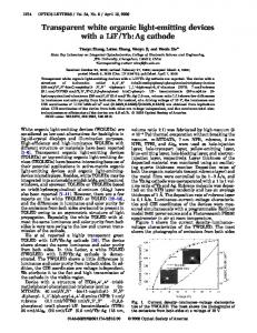
White phosphorescent organic light-emitting devices with dual triple-doped emissive layers Sang-Hyun Eom, Ying Zheng, Edward Wrzesniewski, Jaewon Lee, Neetu Chopra et al. Citation: Appl. Phys. Lett. 94, 153303 (2009); doi: 10.1063/1.3120276 View online: http://dx.doi.org/10.1063/1.3120276 View Table of Contents: http://apl.aip.org/resource/1/APPLAB/v94/i15 Published by the AIP Publishing LLC.
Additional information on Appl. Phys. Lett. Journal Homepage: http://apl.aip.org/ Journal Information: http://apl.aip.org/about/about_the_journal Top downloads: http://apl.aip.org/features/most_downloaded Information for Authors: http://apl.aip.org/authors
Downloaded 28 Sep 2013 to 125.39.171.194. This article is copyrighted as indicated in the abstract. Reuse of AIP content is subject to the terms at: http://apl.aip.org/about/rights_and_permissions
APPLIED PHYSICS LETTERS 94, 153303 共2009兲
White phosphorescent organic light-emitting devices with dual triple-doped emissive layers Sang-Hyun Eom, Ying Zheng, Edward Wrzesniewski, Jaewon Lee, Neetu Chopra, Franky So, and Jiangeng Xuea兲 Department of Materials Science and Engineering, University of Florida, Gainesville, Florida 32611-6400, USA
共Received 11 February 2009; accepted 18 March 2009; published online 16 April 2009兲 We demonstrate high efficiency white organic light-emitting devices with two adjacent emissive layers each doped with three phosphorescent emitters 共blue, green, and red兲. Efficient charge and exciton confinement is realized by employing charge transport layers with high triplet energy, leading to a maximum external quantum efficiency of 共19⫾ 1兲%. Using the p-i-n device structure, we have achieved a peak power efficiency of 共40⫾ 2兲 lm/ W and 共36⫾ 2兲 lm/ W at 100 cd/ m2, a color rendering index of 79, and Commission Internationale de L’Eclairage coordinates of 共0.37, 0.40兲 for the white light emission. © 2009 American Institute of Physics. 关DOI: 10.1063/1.3120276兴 There have been many different approaches to achieving efficient white phosphorescent organic light-emitting devices 共PHOLEDs兲 for solid-state lighting and display applications.1–6 These devices have now surpassed incandescent light bulbs in terms of efficiency and lifetime.2–4 Active research has been focused on further improving their device efficiency to beyond that of fluorescent lights 共60–90 lm/W兲 and achieving high color rendering indices 共CRI兲. Su et al.6 recently reported high efficiency white PHOLEDs with a peak power efficiency 共 P兲 of 58 lm/W using two phosphorescent dopants, a greenish-blue emitter, iridium共III兲 bis关共4,6-difluorophenyl兲-pyridinato-N , C2⬘兴picolinate 共FIrpic兲 共Ref. 7兲 and a red emitter, iridium共III兲 bis-共2-phenylquinolyN , C2⬘兲dipivaloylmethane 共PQ2Ir兲. Due to the limited spectral coverage of the two emitters, that device possessed a low CRI of 68 despite the high efficiencies. In a previous work by D’Andrade et al.,8 a much higher CRI of 80 could be obtained by using three emitters, a deep-blue dye, iridium共III兲 bis共4⬘ , 6⬘-difluorophenylpyridinato兲tetrakis共1pyrazolyl兲borate 共FIr6兲,9 in addition to the red emitter, iridium共III兲 bis-共2-phenylquinolyl-N , C2⬘兲 acetylacetonate 共PQIr兲, and the green emitter, fac-tris-共phenylpyridine兲 iridium 关Ir共ppy兲3兴. However, the triplet energy 共T1兲 of FIr6 is higher that of FIrpic 共2.72 eV versus 2.62 eV兲,9 which makes it more difficult to efficiently generate and confine excitons on the deep-blue emitting FIr6 molecules, leading to a relatively low external quantum efficiency 共EQE兲 of 12% at peak.2,10 We have recently shown that the peak EQE of PHOLEDs based on FIr6 could be improved up to 20% by using 1,1-bis-共di-4-tolylaminophenyl兲cyclohexane 共TAPC兲 as the hole transporting layer 共HTL兲 and tris关3-共3pyridyl兲mesityl兴borane 共3TPYMB兲 as the electron transporting layer 共ETL兲.11,12 The efficiency improvements are attributed to the enhanced charge and exciton confinement in the emissive layer 共EML兲 provided by the charge transport layers. Furthermore, we have employed the dual-EML 共D-EML兲 structure to maximize exciton generation and the p-i-n dea兲
Author to whom correspondence should be addressed. Electronic mail:
[email protected].
0003-6951/2009/94共15兲/153303/3/$25.00
vice structure to minimize the device operating voltage, leading to P = 36 lm/ W at peak for such deep-blue PHOLEDs.12,13 Here, we report highly efficient white PHOLEDs by incorporating green and red phosphorescent dopants along with FIr6 into the D-EML p-i-n PHOLEDs. We have achieved a maximum EQE = 共19⫾ 1兲% and a maximum P = 共40⫾ 2兲 lm/ W without any outcoupling enhancement technique. With balanced emission from the three emitters, the white light emission has a CRI of 79 and Commission Internationale de L’Eclairage 共CIE兲 coordinates of 共0.37, 0.40兲. The OLEDs were fabricated on glass substrates precoated with an indium tin oxide 共ITO兲 anode 共sheet resistance ⬃20 ⍀ / 䊐兲 using vacuum thermal evaporation following procedures published previously.12,13 The general structure for p-i-n devices is ITO/hole injection layer 共HIL兲/ HTL/EML/ETL/electron injection layer 共EIL兲/cathode, in which the p-type HIL and the n-type EIL13,14 consisted of N , N⬘-diphenyl-N , N⬘-bis共3-methylphenyl兲-关1 , 1⬘biphenyl兴-4 , 4⬘-diamine 共MeO-TPD兲 doped with 2 mol % and tetrafluoro-tetracyanoquinodimethane 共F4-TCNQ兲 3TPYMB doped with Cs 共with a molar ratio of 1:0.3兲, respectively, whereas TAPC and 3TPYMB served as the HTL and ETL, respectively. Conventional devices without the HIL and EIL were also fabricated as a comparison. Two wide-gap hosts, N , N⬘-dicarbazolyl-3,5-benzene 共mCP兲2,13 and p-bis共triphenylsilyly兲benzene 共UGH2兲,8,10 each doped with the three phosphorescent dopants 共FIr6, Ir共ppy兲3, and PQIr兲, were used to form the D-EML structure. In contrast, the mCP layer was undoped in the single-EML 共S-EML兲 devices. The cathode consisting of a 0.5 nm thick LiF followed by a 50 nm thick Al was deposited through an in situ shadow mask, forming active device area of 4 mm2. The structures and layer thicknesses of the specific devices to be discussed below are summarized in Table I. Luminance 共L兲-current density 共J兲-voltage 共V兲 and electroluminescent 共EL兲 spectral measurements were carried out in ambient without encapsulation. The luminous, power, and external quantum efficiencies 共L, P, and EQE, respectively兲 were derived based on the previously published methods.15 Note that all efficiency values referred to here are for emissions in
94, 153303-1
© 2009 American Institute of Physics
Downloaded 28 Sep 2013 to 125.39.171.194. This article is copyrighted as indicated in the abstract. Reuse of AIP content is subject to the terms at: http://apl.aip.org/about/rights_and_permissions
153303-2
Appl. Phys. Lett. 94, 153303 共2009兲
Eom et al.
TABLE I. List of device structures and layer thicknesses. The general device structure is ITO/HIL/HTL/EML/ ETL/EIL/cathode, where HIL= hole injection layer, HTL= hole transport layer, EML= emissive layer, ETL = electron transport layer, and EIL= electron injection layer.
Device A B C
HIL 共nm兲
HTL 共nm兲
EML
ETL 共nm兲
EIL 共nm兲
¯ ¯ 30
40 40 10
S-EMLa D-EMLb D-EMLb
40 40 10
¯ ¯ 30
S-EML= mCP 共10 nm, undoped兲/UGH2共20 nm, doped兲. D-EML= mCP 共7 nm, doped兲/UGH2共10 nm, doped兲.
a
b
the forward-viewing directions without any specific outcoupling enhancement technique.2 Figure 1 illustrates possible energy transfer paths among the dopants in the two wide-gap hosts, as well as exciton confinement by TAPC and 3TPYMB 共energy levels are taken from the literature兲.9,12,16 The triplet energies of TAPC 共T1 = 2.87 eV兲 共Ref. 11兲 and 3TPYMB 共T1 = 2.95 eV兲 共Ref. 16兲 are higher than that of FIr6 共T1 = 2.72 eV兲 共Ref. 9兲 leading to effective confinement of triplet excitons within the two EMLs.13 The optimized D-EML structure consists of a 10 nm thick UGH2 layer and a 7 nm thick mCP layer where the FIr6, Ir共ppy兲3, and PQIr doping concentrations are 25, 2.5, and 2.3 wt %, respectively, in UGH2, and 5.0, 1.3, and 1.0 wt %, respectively, in mCP. Figure 2共a兲 compares J-V characteristics of conventional S-EML 共device A兲 and D-EML 共device B兲 white PHOLEDs, whereas P and EQE of these two devices are compared in Fig. 2共b兲. The maximum external quantum efficiencies of these two devices are almost the same, EQE,max = 共19⫾ 1兲%. However, the maximum power efficiency is P,max = 共31⫾ 2兲 lm/ W for device A and 共38⫾ 2兲 lm/ W for device B. The greater thickness of the UGH2 layer in device A 共20 nm兲 versus 10 nm in device B results in significantly higher
FIG. 1. 共Color online兲 Molecular structure of three phosphorescent dopants and triplet energy 共T1兲 levels of materials involved in a dual-emissive-layer white PHOLED. Possible energy flow in the device is also shown. Energy levels are taken from the literature.
operating voltages for the former device. However, reducing the UGH2 layer thickness in the S-EML structure to below 20 nm leads to a significant decrease in EQE due to the incomplete charge recombination in the thinner EML.13 The EL spectra of both devices are shown in the inset of Fig. 2共a兲. The significantly reduced blue emission of device A may be attributed to strong charge trapping by the green and red dopants, leading to inefficient exciton formation on the blue dopant. Different from the UGH2 layer in which charge transport is through the dopant molecules,10 the mCP molecules participate in charge transport, leading to a stronger blue emission component in the D-EML device. Note that while the CIE coordinates of device B at 100 cd/ m2 are 共0.37, 0.40兲, which are similar to those of fluorescent lights, the D-EML white PHOLED possesses a CRI of 79, much higher than fluorescent lights 共CRI⬇ 60兲.17 Although device B shows a high EQE and relatively low turn-on voltage of VT = 3.2 V, the peak P is achieved at a low current density of J ⬍ 10−2 mA/ cm2. In order to improve P at higher luminances, we employed the p-i-n device structure to reduce the device voltage.12,13 As shown in the inset of Fig. 3, the current density of the p-i-n device 共device C兲 is one to two orders of magnitude higher than that of device B 共at V ⬎ 3 V兲. The p-i-n device has a lower VT
FIG. 2. 共Color online兲 共a兲 Current density-voltage 共J-V兲 characteristics of single- and dual-emissive-layer 共devices A and B, respectively兲 conventional white PHOLEDs. See Table I for detailed device structures. 共Inset兲 EL spectra of these two devices. 共b兲 Power 共 P兲 and external quantum 共EQE兲 efficiencies as a function of current density 共J兲 for these two devices.
Downloaded 28 Sep 2013 to 125.39.171.194. This article is copyrighted as indicated in the abstract. Reuse of AIP content is subject to the terms at: http://apl.aip.org/about/rights_and_permissions
153303-3
Appl. Phys. Lett. 94, 153303 共2009兲
Eom et al.
FIG. 3. 共Color online兲 Power efficiency 共 P兲 of a dual-emissive-layer p-i-n white PHOLED 共device C兲 compared to device B. See Table I for detailed device structures. 共Inset兲 Current density-voltage 共J-V兲 characteristics of these two devices.
= 2.9 V and the operating voltages at 100 and 1000 cd/ m2 are 3.5 and 4.0 V, respectively. Even though the peak EQE of p-i-n device is slightly reduced to 共18⫾ 1兲%, a higher maximum P of 共40⫾ 2兲 lm/ W is achieved 共see Fig. 3兲. The power efficiencies at L = 100 and 1000 cd/ m2 are P = 共36⫾ 2兲 and 共26⫾ 2兲 lm/ W, respectively, approximately 30% higher than that for device B at the same luminances. Moreover, P of our devices are more than twice higher than those of the triple-doped device reported by D’Andrade et al.,8 in which P = 11 lm/ W at L = 1000 cd/ m2. The performance of our device also shows improvement over that of the device by Sun and Forrest,5 in which the same three dopants were separately doped into three adjacent EMLs and
FIG. 4. 共Color online兲 EL spectra of a dual-emissive-layer p-i-n white PHOLED 共device C兲 at luminance of L = 10, 100, and 1000 cd/ m2.
showed P = 38 lm/ W at peak and 20 lm/W at L = 1000 cd/ m2. Figure 4 shows the EL spectra of device C at different luminances. With the increase in luminance, the relative intensity of the blue emission slightly increases, while that of the red emission slightly decreases, leading to a slight shift in the CIE coordinates from 共0.39, 0.41兲 at L = 10 cd/ m2 to 共0.35, 0.40兲 at L = 1000 cd/ m2. The CRI of the device remains at 79⫾ 1, which is approximately the same as that of the previously reported devices using the same three dopants,5,8 but is significantly higher than that of the device by Su et al.6 using two dopants. In conclusion, we have demonstrated high efficiency white PHOLEDs by codoping three phosphorescent dopants into two adjacent EMLs. High external quantum efficiencies of 18%–19% are achieved with high triplet energy materials as the charge transport layers. Using the p-i-n device structure to reduce the operating voltage, we have achieved a peak power efficiency of 共40⫾ 2兲 lm/ W with a high CRI of 79⫾ 1. This work was supported by the U.S. Department of Energy Solid State Lighting Program 共Award No. DE-FC2606NT42855兲. S.H.E. also acknowledges a fellowship from Samsung SDI. Co., Ltd. S. R. Forrest, Nature 共London兲 428, 911 共2004兲. B. W. D’Andrade and S. R. Forrest, Adv. Mater. 共Weinheim, Ger.兲 16, 1585 共2004兲. 3 Y. Sun, N. C. Giebink, H. Kanno, B. W. Ma, M. E. Thompson, and S. R. Forrest, Nature 共London兲 440, 908 共2006兲. 4 E. L. Williams, K. Haavisto, J. Li, and G. E. Jabbour, Adv. Mater. 共Weinheim, Ger.兲 19, 197 共2007兲. 5 Y. Sun and S. R. Forrest, Appl. Phys. Lett. 91, 263503 共2007兲. 6 S.-J. Su, E. Gonmori, H. Sasabe, and J. Kido, Adv. Mater. 共Weinheim, Ger.兲 20, 4189 共2008兲. 7 R. J. Holmes, S. R. Forrest, Y.-J. Tung, R. C. Kwong, J. J. Brown, S. Garon, and M. E. Thompson, Appl. Phys. Lett. 82, 2422 共2003兲. 8 B. W. D’Andrade, R. J. Holmes, and S. R. Forrest, Adv. Mater. 共Weinheim, Ger.兲 16, 624 共2004兲. 9 X. Ren, J. Li, R. J. Holmes, P. I. Djurovich, S. R. Forrest, and M. E. Thompson, Chem. Mater. 16, 4743 共2004兲. 10 R. J. Holmes, B. W. D’Andrade, S. R. Forrest, X. Ren, J. Li, and M. E. Thompson, Appl. Phys. Lett. 83, 3818 共2003兲. 11 Y. Zheng, S.-H. Eom, N. Chopra, J. Lee, F. So, and J. Xue, Appl. Phys. Lett. 92, 223301 共2008兲. 12 S.-H. Eom, Y. Zheng, E. Wrzesniewski, J. Lee, N. Chopra, F. So, and J. Xue, “Effect of electron injection and transport materials on efficiency of deep-blue phosphorescent organic light-emitting devices,” Org. Electron. 共in press兲. 13 S.-H. Eom, Y. Zheng, N. Chopra, J. Lee, F. So, and J. Xue, Appl. Phys. Lett. 93, 133309 共2008兲. 14 G. He, M. Pfeiffer, K. Leo, M. Hofmann, J. Birnstock, R. Pudzich, and J. Salbeck, Appl. Phys. Lett. 85, 3911 共2004兲. 15 S. R. Forrest, D. D. C. Bradley, and M. E. Thompson, Adv. Mater. 共Weinheim, Ger.兲 15, 1043 共2003兲. 16 D. Tanaka, T. Takeda, T. Chiba, S. Watanabe, and J. Kido, Chem. Lett. 36, 262 共2007兲. 17 K. Sakuma, N. Hirosaki, N. Kimura, M. Ohashi, R.-J. Xie, Y. Yamamoto, T. Suehiro, K. Asano, and D. Tanaka, IEICE Trans. Electron. E88-C, 2057 共2005兲. 1 2
Downloaded 28 Sep 2013 to 125.39.171.194. This article is copyrighted as indicated in the abstract. Reuse of AIP content is subject to the terms at: http://apl.aip.org/about/rights_and_permissions